
Lab 7 - EE 421L: Digital Integrated Circuit
Design Laboratory
Using buses and arrays in the design of word inverters, muxes, and high-speed adders
Lab Work
Post-Lab Scope
Below
are the pre-lab deliverables.
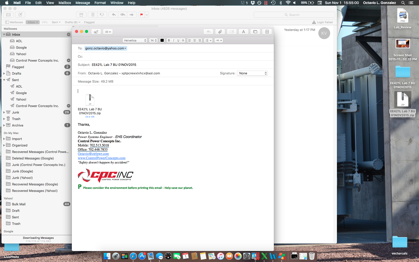
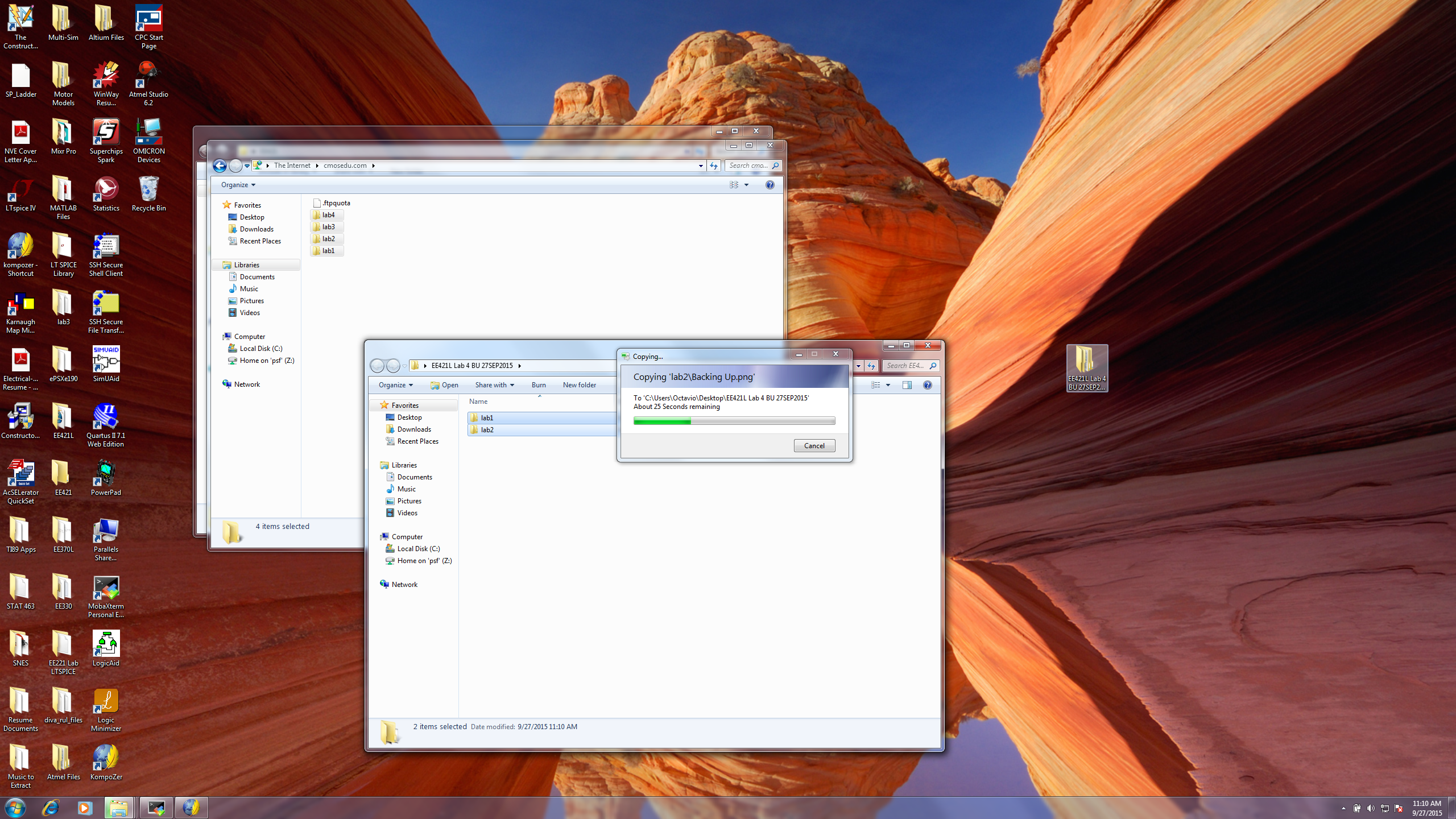
As can be seen, before starting, backing up all the work from the EE421 Lab and Course is required.
Saving the CMOSedu Directory Files to Folder EE421L Lab 7 BU 01NOV2015 on the Desktop
Emailing EE421L Lab 7 BU 01NOV2015 Zip to gonzao1@unlv.nevada.edu
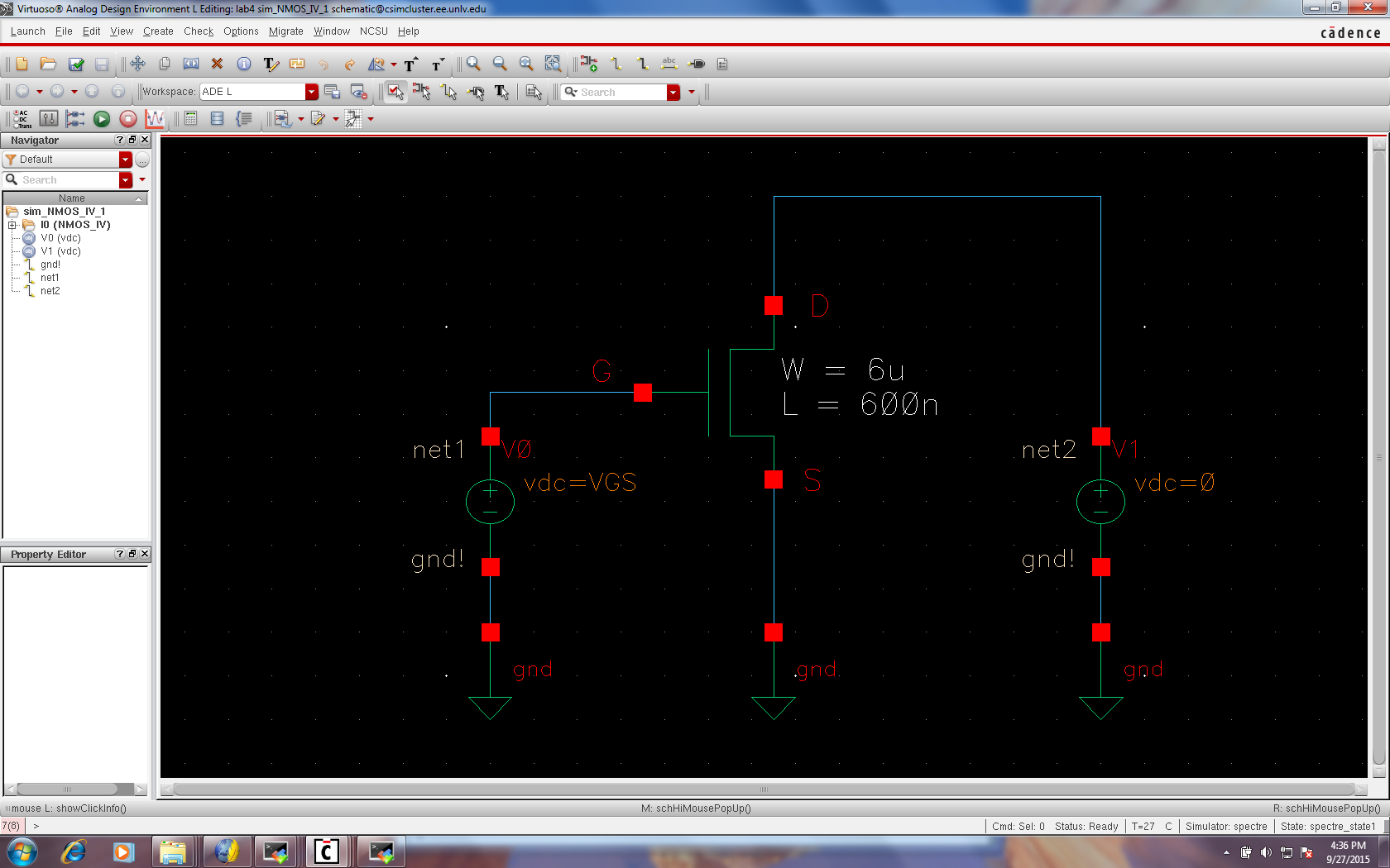
Below is a screenshot of reading through the Lab 7 requirements and scope prior to starting the assignment.

Tutorial 5
As can be seen below, Tutorial 5 has been completed. Note: LVS and DRC without errors.

Post-Lab:
Below are the post-lab deliverables.
The following are a few simulation examples using NAND, NOR, AND, inverter, and OR gates.
Below is the 8-Bit NAND gate Schematic.

Below is the 8-Bit NAND gate Simulation.

Below is the 8-Bit NOR gate Schematic.

Below is the 8-Bit NOR gate Simulation.

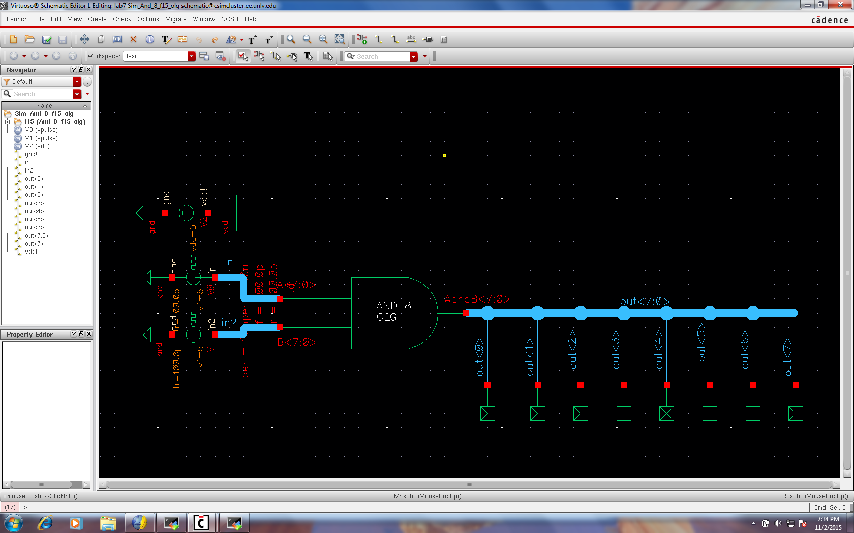
Below is the 8-Bit AND gate Schematic.
Below is the 8-Bit AND gate Simulation.

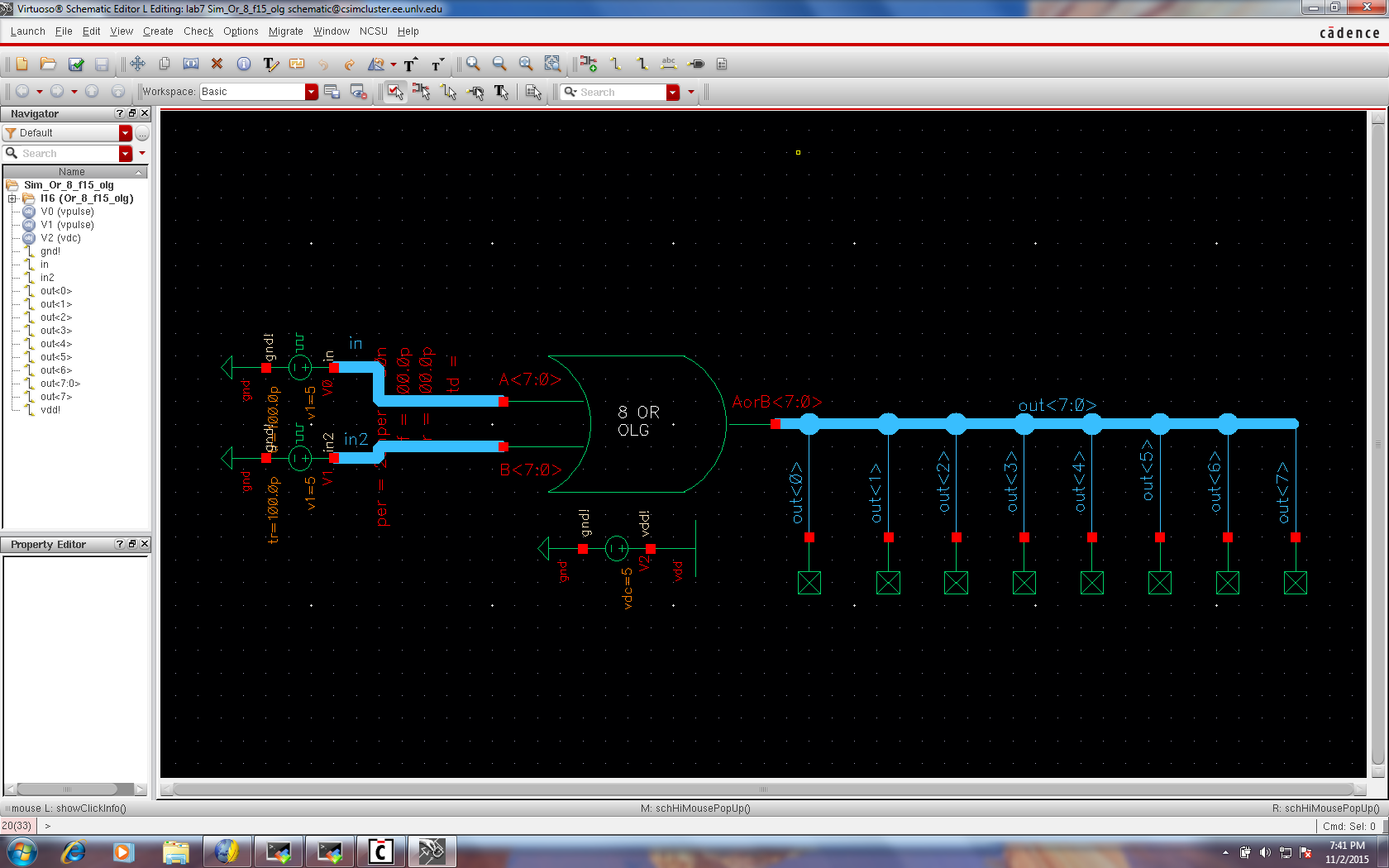
Below is the 8-Bit OR gate Schematic.
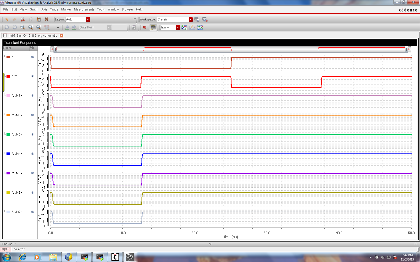
Below is the 8-Bit OR gate Simulation.
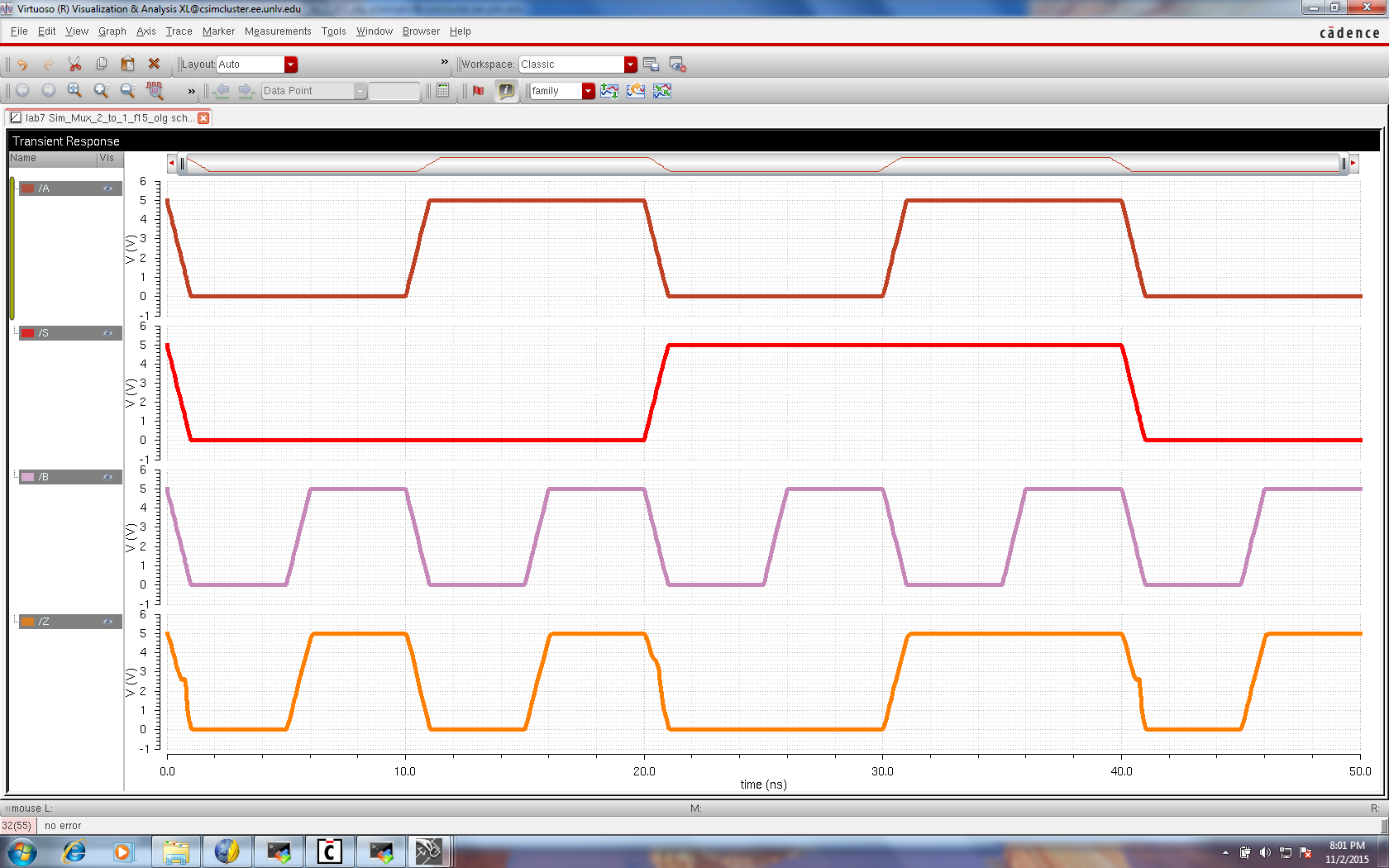
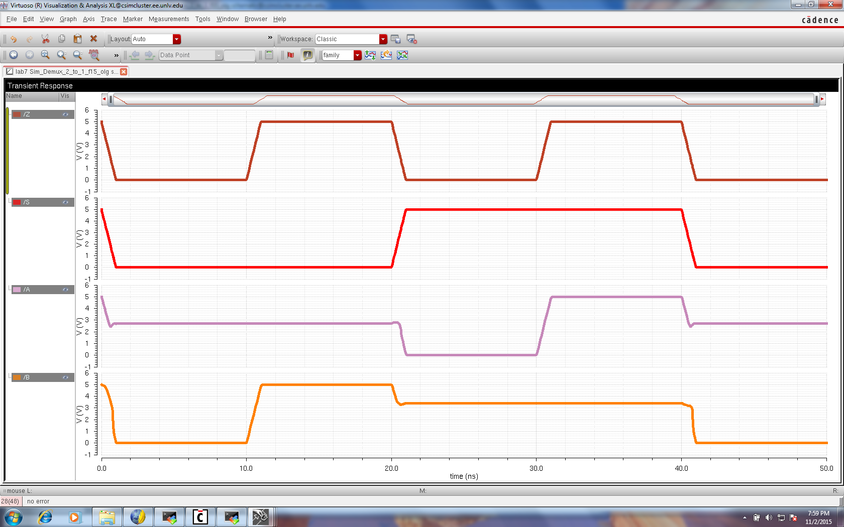
The following is a simulation on the operation of a 2-to-1 DEMUX/MUX using Spectre as well as an explaination on how it works.
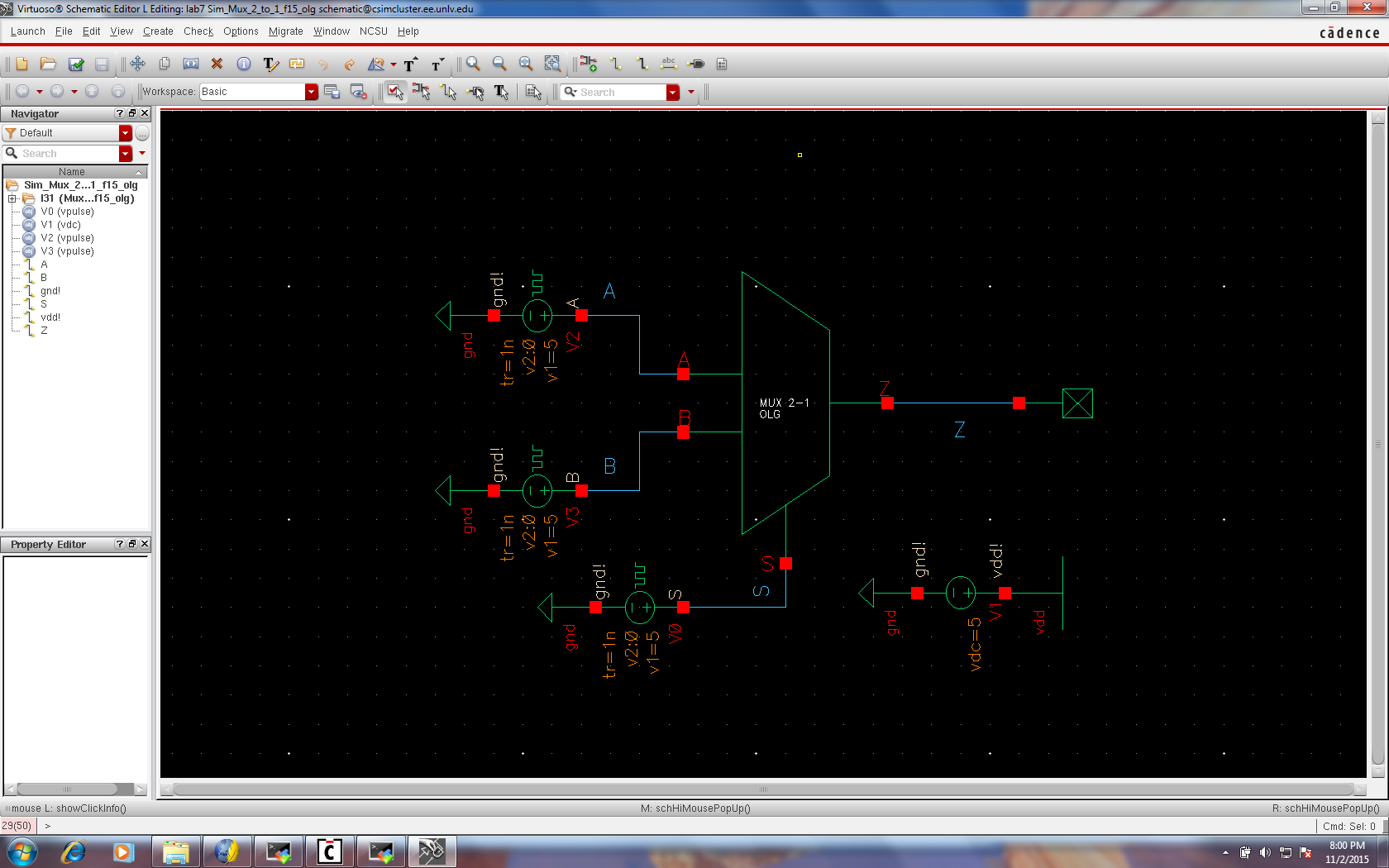
Below is the 2-Bit MUX Schematic.
Below is the 2-Bit MUX Simulation.
Below is the 2-Bit DEMUX Schematic.

Below is the 2-Bit DEMUX Simulation.
8-Bit Wide Word:
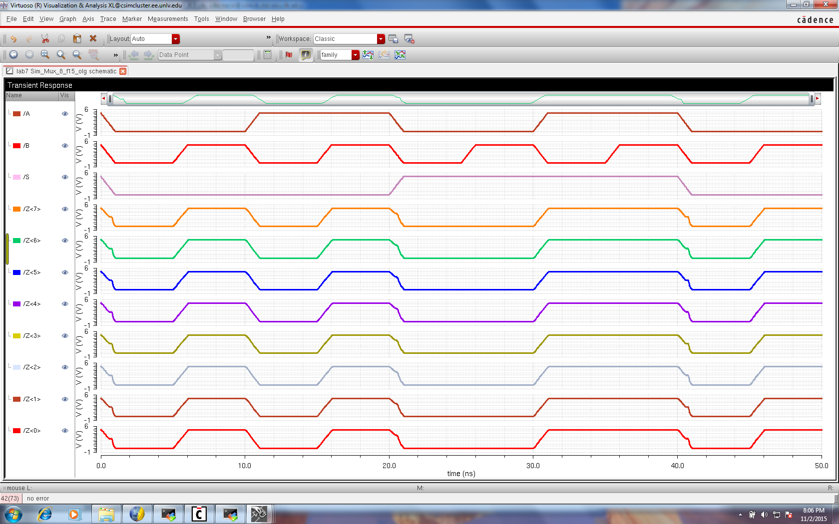
The following is a simulation of the 8-bit wide word 2-to-1 DEMUX/MUX schematic and symbol..
Below is the 8-Bit MUX Schematic.

Below is the 8-Bit MUX Simulation.
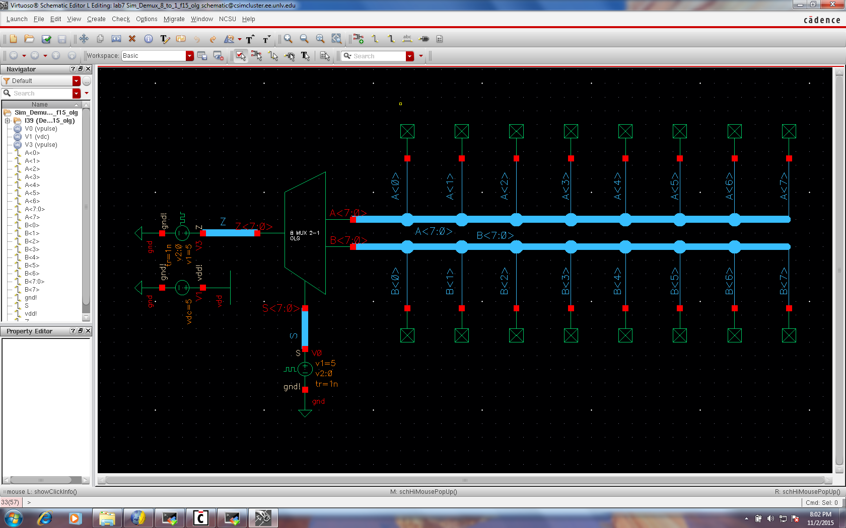
Below is the 8-Bit DEMUX Schematic.
Below is the 8-Bit DEMUX Simulation.

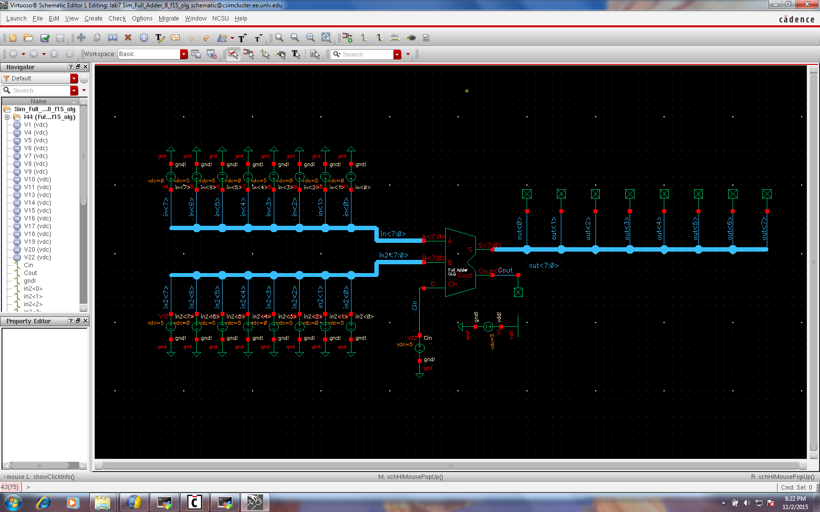
The following is the Full-Adder Schematic and Symbol

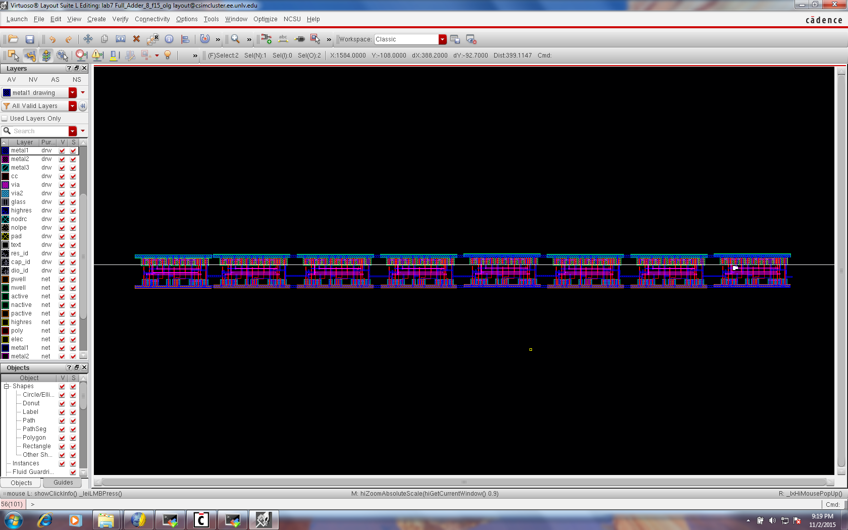
The following is theLayout and Extracted Layout DRC/LVS Verifications for the Full-Adder

The webpage and design directory was backed-up during the pre-lab portion of the lab.
Lab 7 served as a means to design, layout, and simulate a Full-Adder using the ON's C5 process.