Lab 6 - EE 421L: Digital Integrated Circuit
Design Laboratory
Octavio
L. Gonzalez
gonzao1@unlv.nevada.edu
12OCT2015
Lab
description:
Design,
layout, and simulation of a CMOS inverter
Pre-Lab Scope
- Back-up all of your work from the lab and the course.
- Go through Cadence Tutorial 4.
- Read through the lab in its entirety before starting to work
on it
Lab Work
- Draft the schematics of a 2-input NAND gate (Fig. 12.1), and a 2-input
XOR gate (Fig. 12.18) using 6u/0.6u MOSFETs (both NMOS and PMOS)
- Create layout and symbol views for these gates showing that the cells
DRC and LVS without errors ensure that your symbol views are the commonly used symbols (not
boxes!) for these gates with your initials in the middle of the
symbol
- Ensure all layouts in this lab use standard cell frames that snap
together end-to-end for routing vdd! and gnd!
- Use a standard cell height taller than you need for these gates so that
it can be used for more complicated layouts in the future.
- Ensure gate inputs, outputs, vdd!, and gnd! are all routed on metal1
- Use cell names that include your initials and the current
year/semester, e.g. NAND_jb_f19 (if it were fall 2019)
- Using Spectre simulate the logical operation of the gates for all 4
possible inputs (00, 01, 10, and 11)
- comment on how timing of the input pulses can cause glitches in the
output of a gate
- Your html lab report should detail each of these efforts
- Using these gates, draft the schematic of a full adder
- Create a symbol for this full-adder
- Simulate, using Spectre, the operation of the full-adder using this symbol
- Layout the full-adder by placing the 5 gates end-to-end so that vdd! and gnd! are routed
- full-adder inputs and outputs can be on metal2 but not metal3
- DRC and LVS your full adder design
Post-Lab Scope
- Using SPICE simulate the
operation of both of your inverters showing each driving a 100 fF, 1
pF, 10 pF, and 100 pF capacitive load.
- Comment, in your
report, on the results
- Zip up these cells in a
directory call lab5_rjb.zip (last two or three letters are your
initials) and link to your lab report.
- As always ensure that
your html lab report includes your name and
email address at the beginning of the report (the top of the webpage).
- When finished backup
your work (webpages and design directory).
Pre-Lab:
Below
are the pre-lab deliverables.
Back-Up Work
As
can be seen, before starting, backing up all the work from the EE421
Lab and Course is required.
Saving
the CMOSedu Directory Files to Folder EE421L Lab 6 BU
17OCT2015 on the Desktop

Emailing
EE421L Lab 6 BU 27SEP2015 Zip to gonzao1@unlv.nevada.edu

Lab 6 Review
Below
is a screenshot of reading through the Lab 6 requirements and scope
prior to starting the assignment.

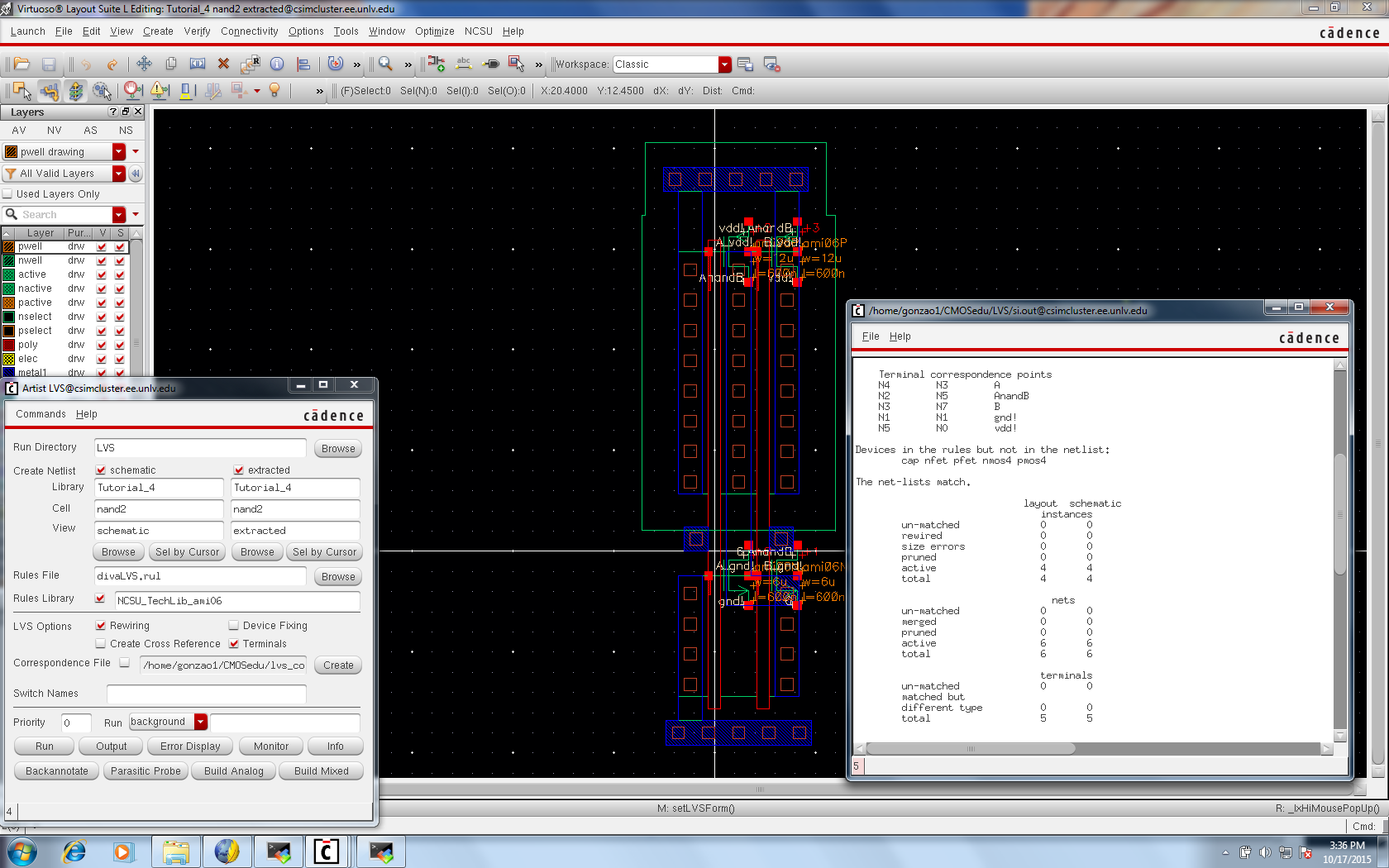
Tutorial 4
As
can be seen below, Tutorial 3 has been completed. Note: LVS without
errors.
Post-Lab:
Below
are the post-lab deliverables.
NAND and XOR Schematics, Layouts, and Symbols
The
following are the Extracted Layout and Schematic DRC/LVS verifications with device symbols
Below is the NAND Gate Schematic
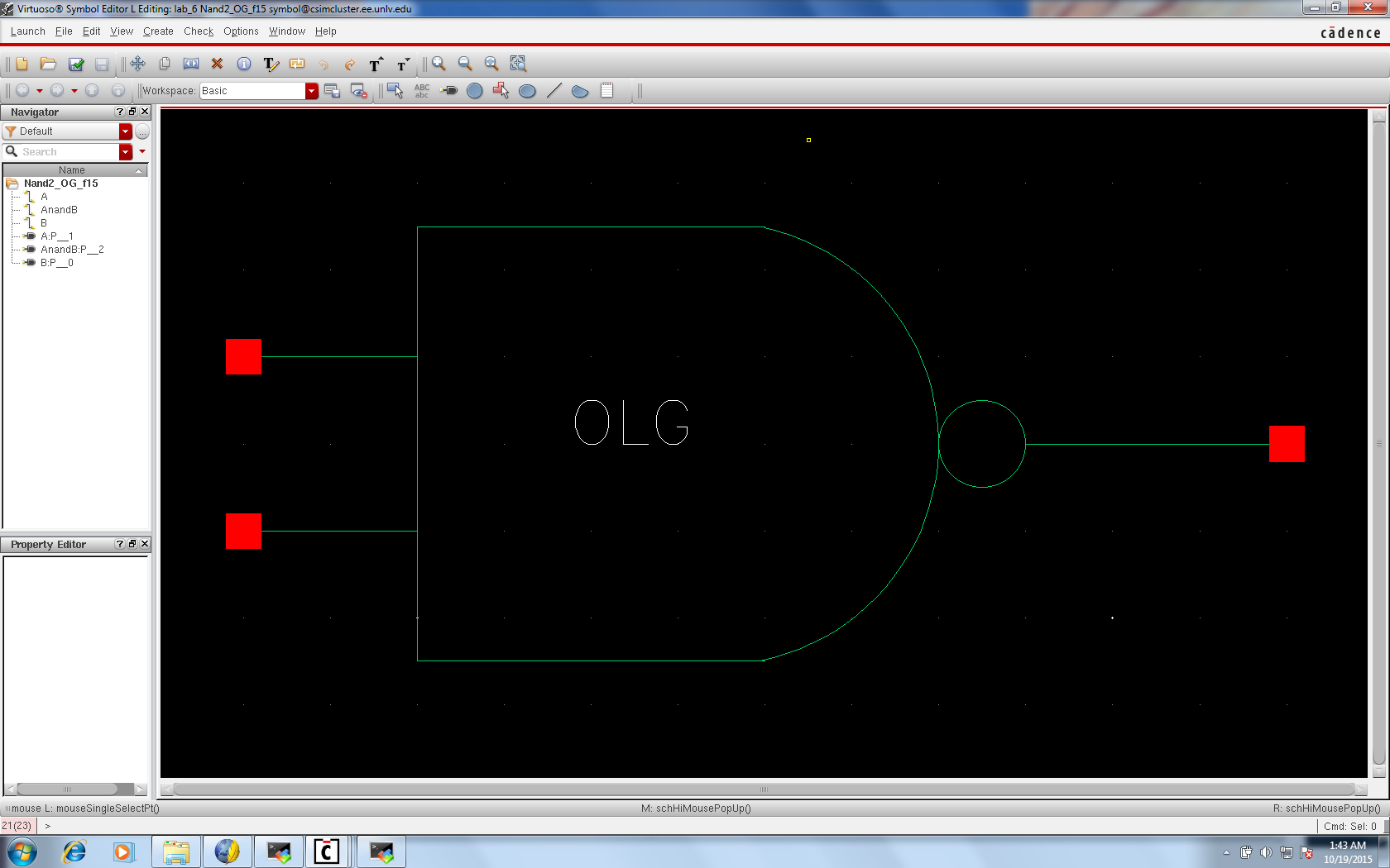
Below is the NAND Gate Symbol
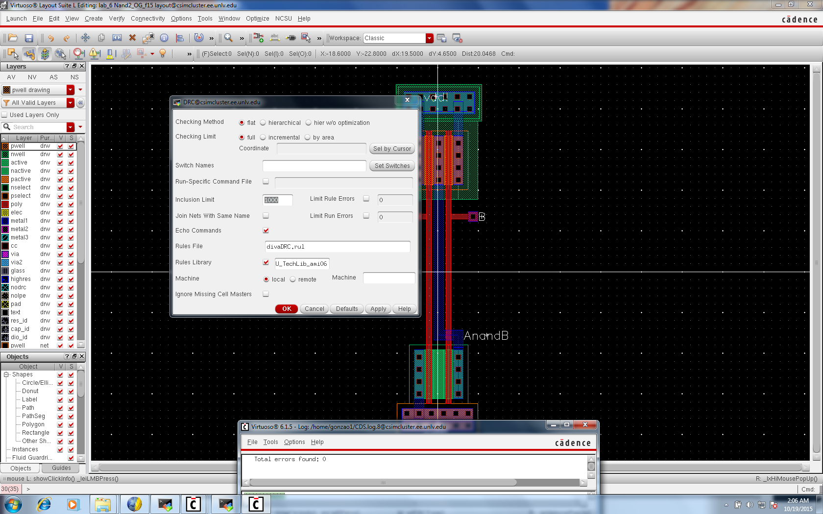
Below is the NAND Gate Layout DRC
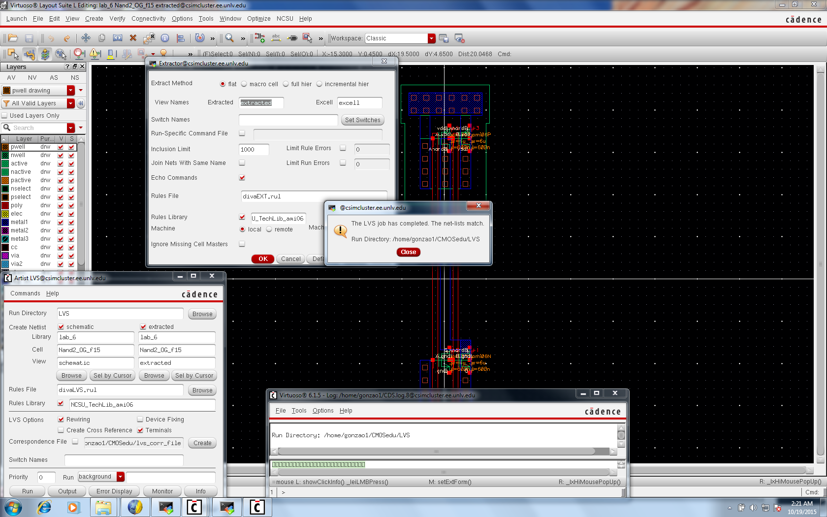
Below is the NAND Gate Extracted Layout LVS
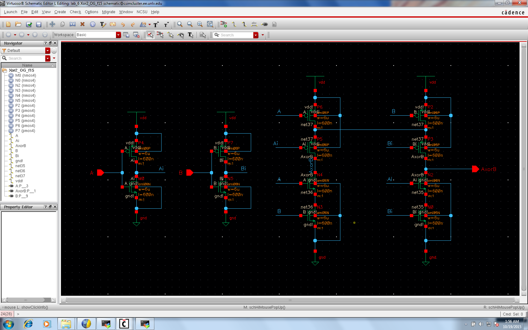
Below is the XOR Gate Schematic
(Need to Request More Data)
Below is the XOR Gate Symbol
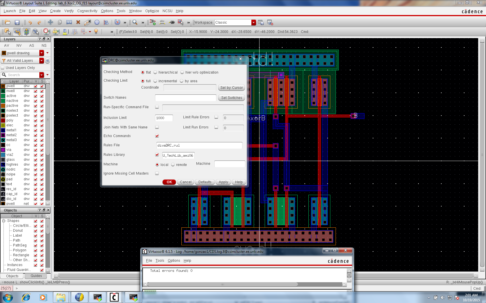
Below is the XOR Gate Layout DRC
Below is the XOR Gate Extracted Layout LVS

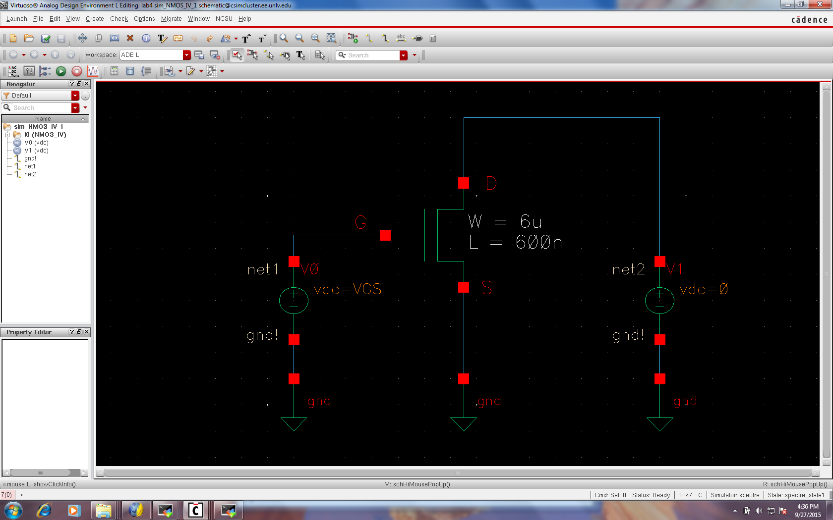
NAND and XOR SPICE Simulations
The
following is the schematic and simulation of the NAND, Inverter, and XOR devices.
Below is the NAND, Inverter, and XOR Simulation Schematic.
Below is the NAND, Inverter, and XOR Simulation Waveform Plot.
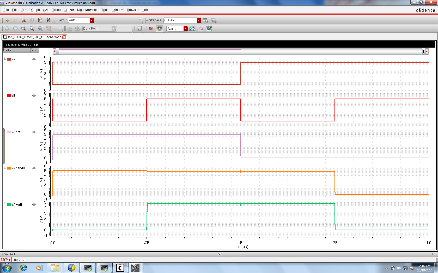
As
can be seen, there are glitches also known as combinational logic
hazards that occur during on/off transitions and switching overlap.
These occur when the propagation delay through a device varies from gate to gate.
Full-Adder Schematic, Layout, and Symbol
The
following is the Extracted Layout and Schematic DRC/LVS verifications with device symbols
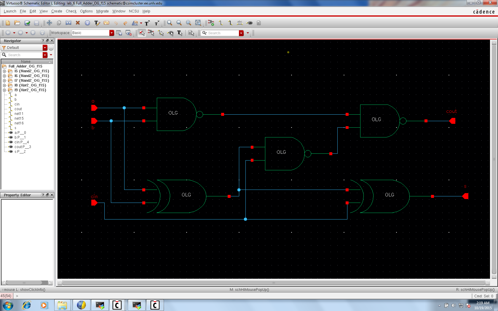
Below is the Full-Adder Gate Schematic
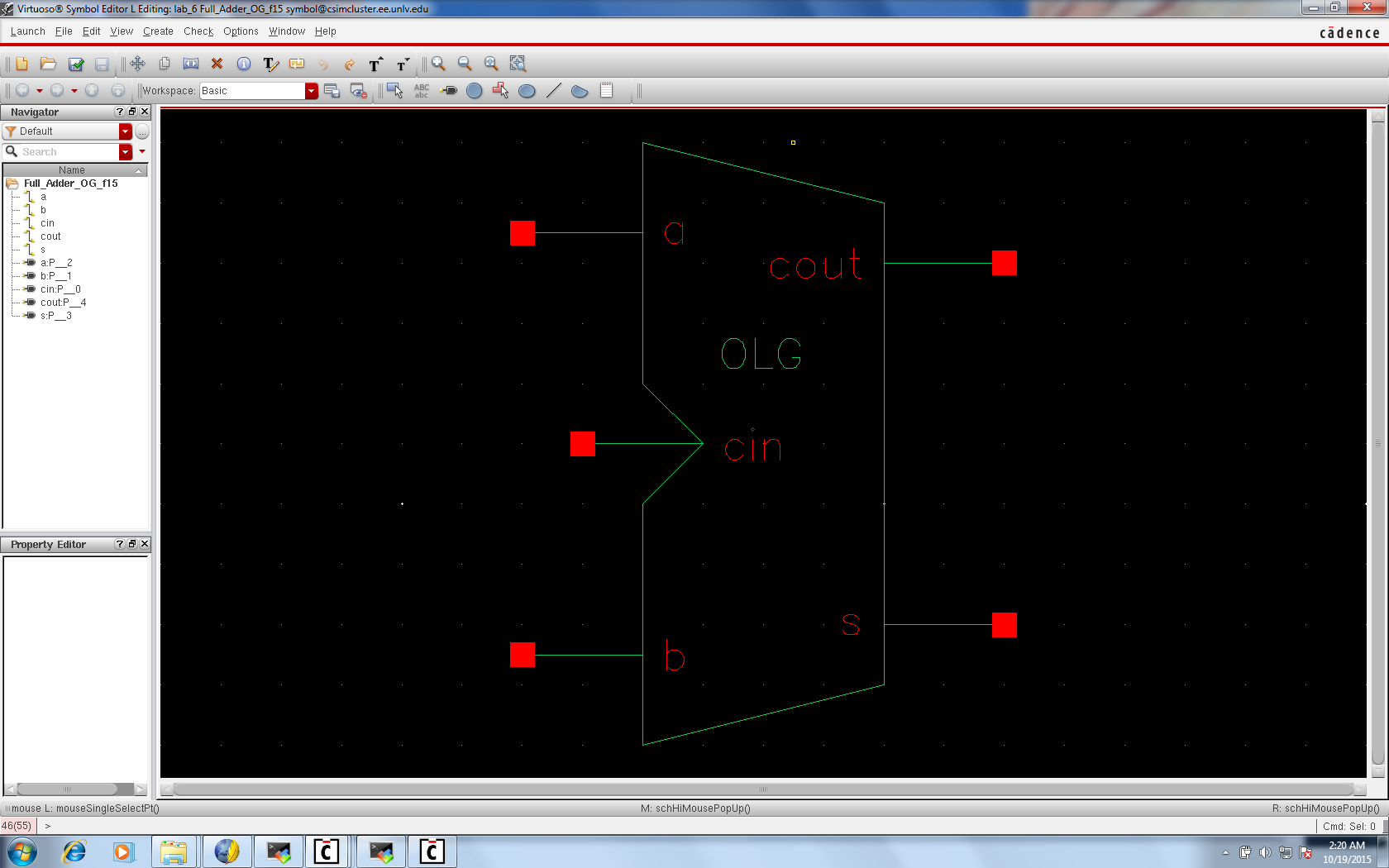
Below is the Full-Adder Gate Symbol
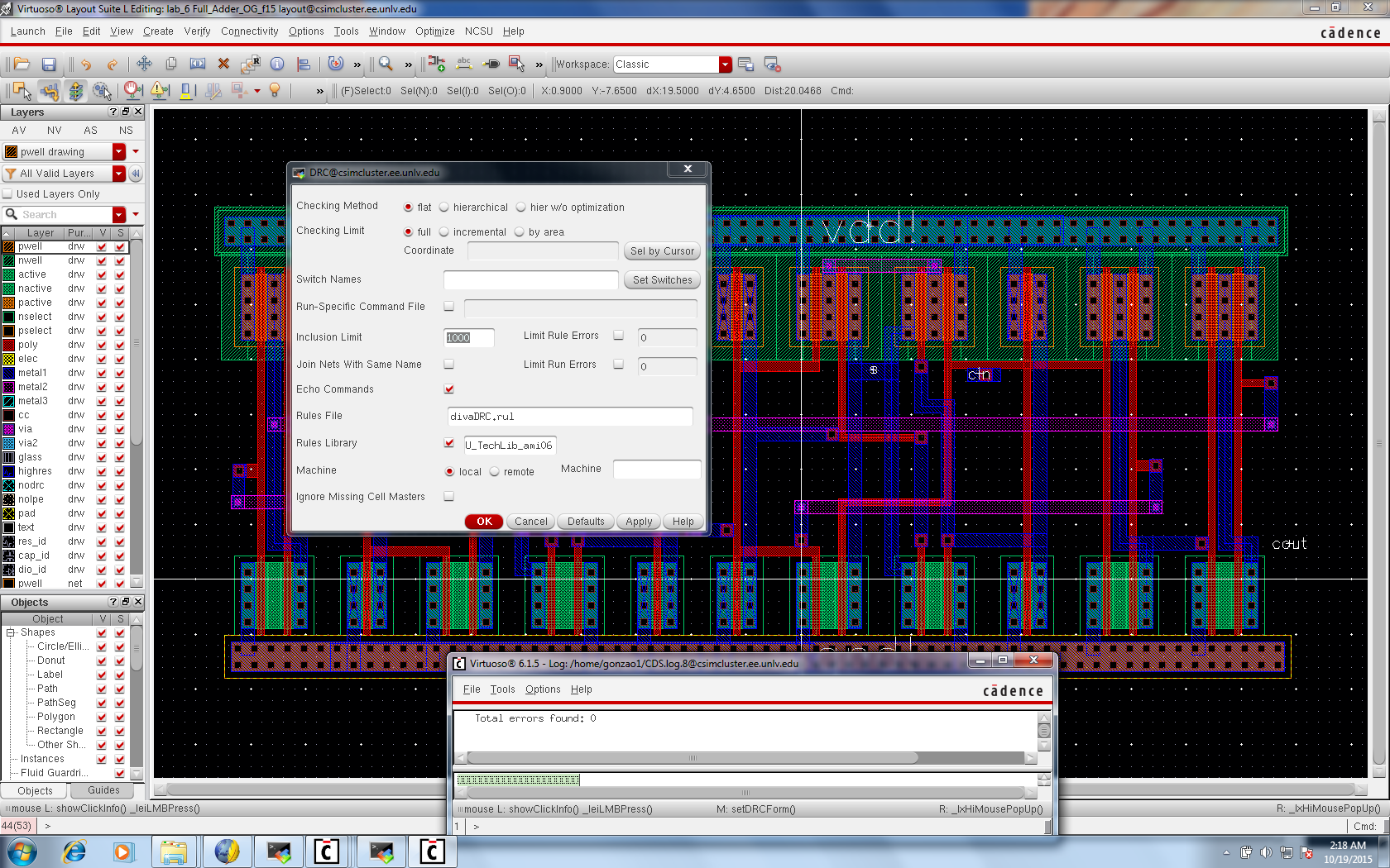
Below is the Full-Adder Gate Layout DRC
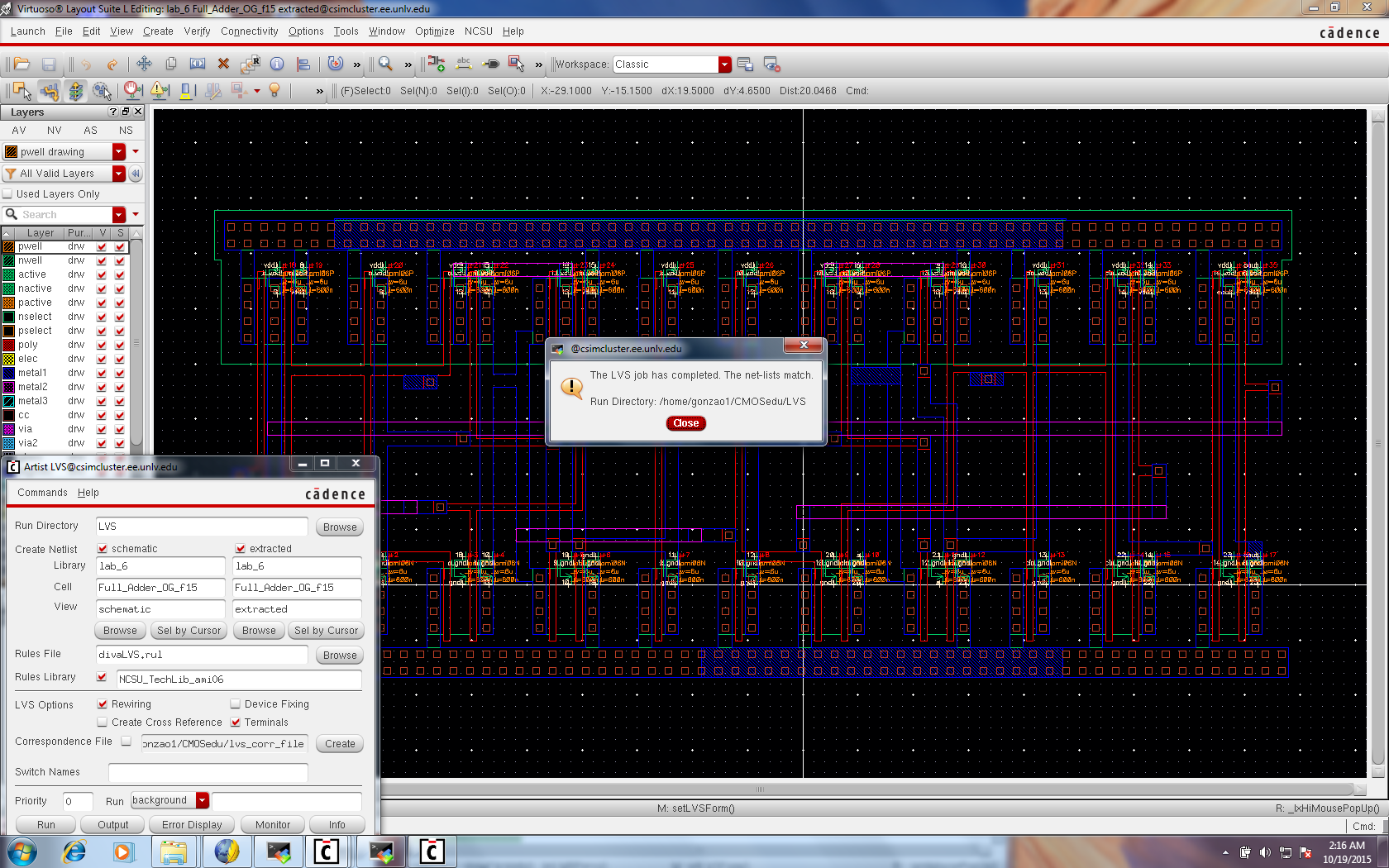
Below is the Full-Adder Gate Extracted Layout LVS
Full-Adder SPICE Simulation
The
following is the schematic and simulation of the Full-Adder device.
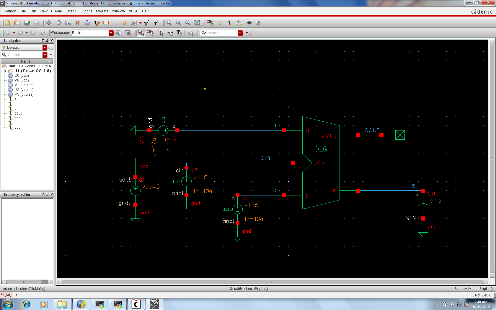
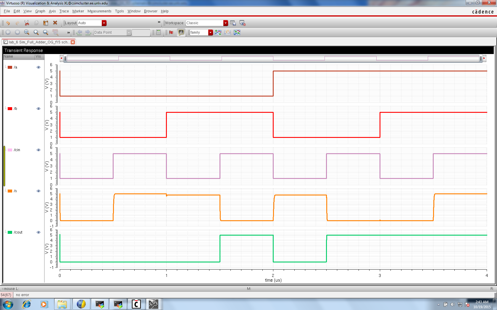
Below is the Full Adder Simulation Schematic.
Below is the Full Adder Simulation Waveform Plot.
Webpage and Design Directory Back-Up
The webpage and design directory was backed-up during the pre-lab portion of the lab.
Conclusion:
Lab 6 served as a means to design,
layout, and simulate a CMOS NAND gate, XOR gate, and Full-Adder in the ON's C5 process.
Return to GONZAO1 lab listings
Return to EE 421L Labs


