
Lab 5 - EE 421L: Digital Integrated Circuit
Design Laboratory
Design,
layout, and simulation of a CMOS inverter
Lab Work
Post-Lab Scope
Below
are the pre-lab deliverables.
As can be seen, before starting, backing up all the work from the EE421 Lab and Course is required.
Saving the CMOSedu Directory Files to Folder EE421L Lab 5 BU 27SEP2015 on the Desktop
Emailing EE421L Lab 5 BU 27SEP2015 Zip to gonzao1@unlv.nevada.edu

Below is a screenshot of reading through the Lab 5 requirements and scope prior to starting the assignment.

Tutorial 3
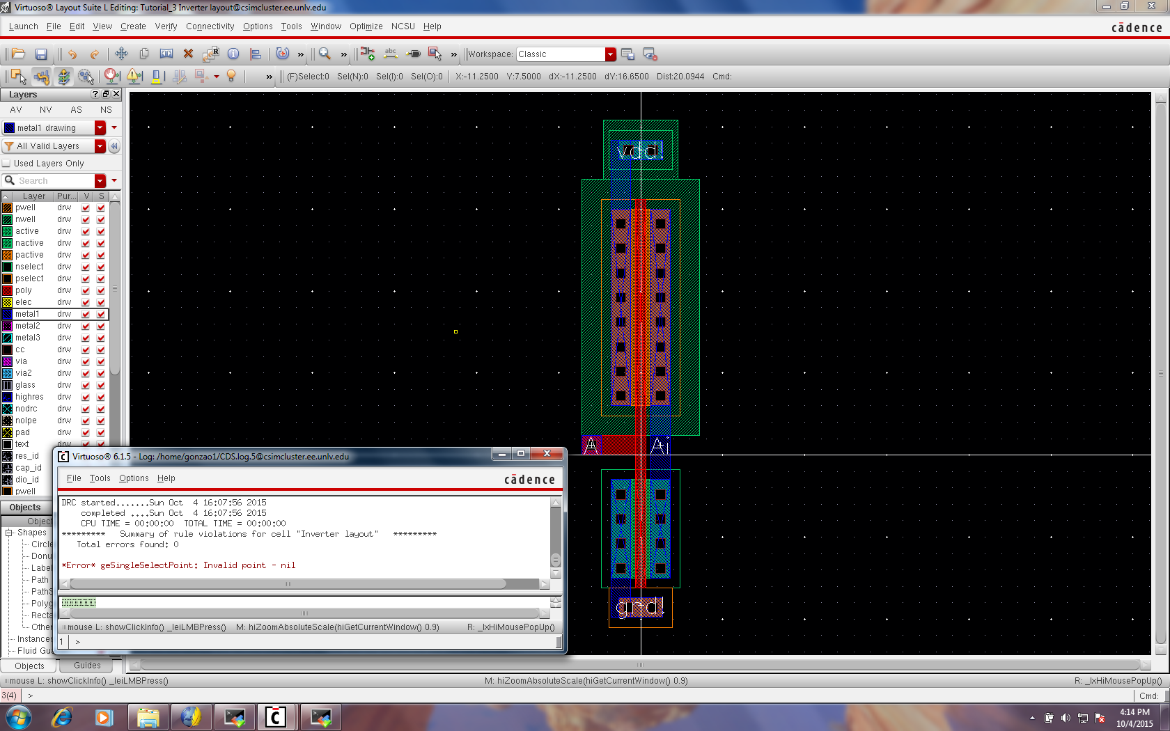
As can be seen below, Tutorial 3 has been completed. Note: LVS without errors.

Post-Lab:
Below are the post-lab deliverables.
The
following are the Extracted Layout and Schematic DRC/LVS Verifications
The following is the 12u/6u Inverter Device Symbol

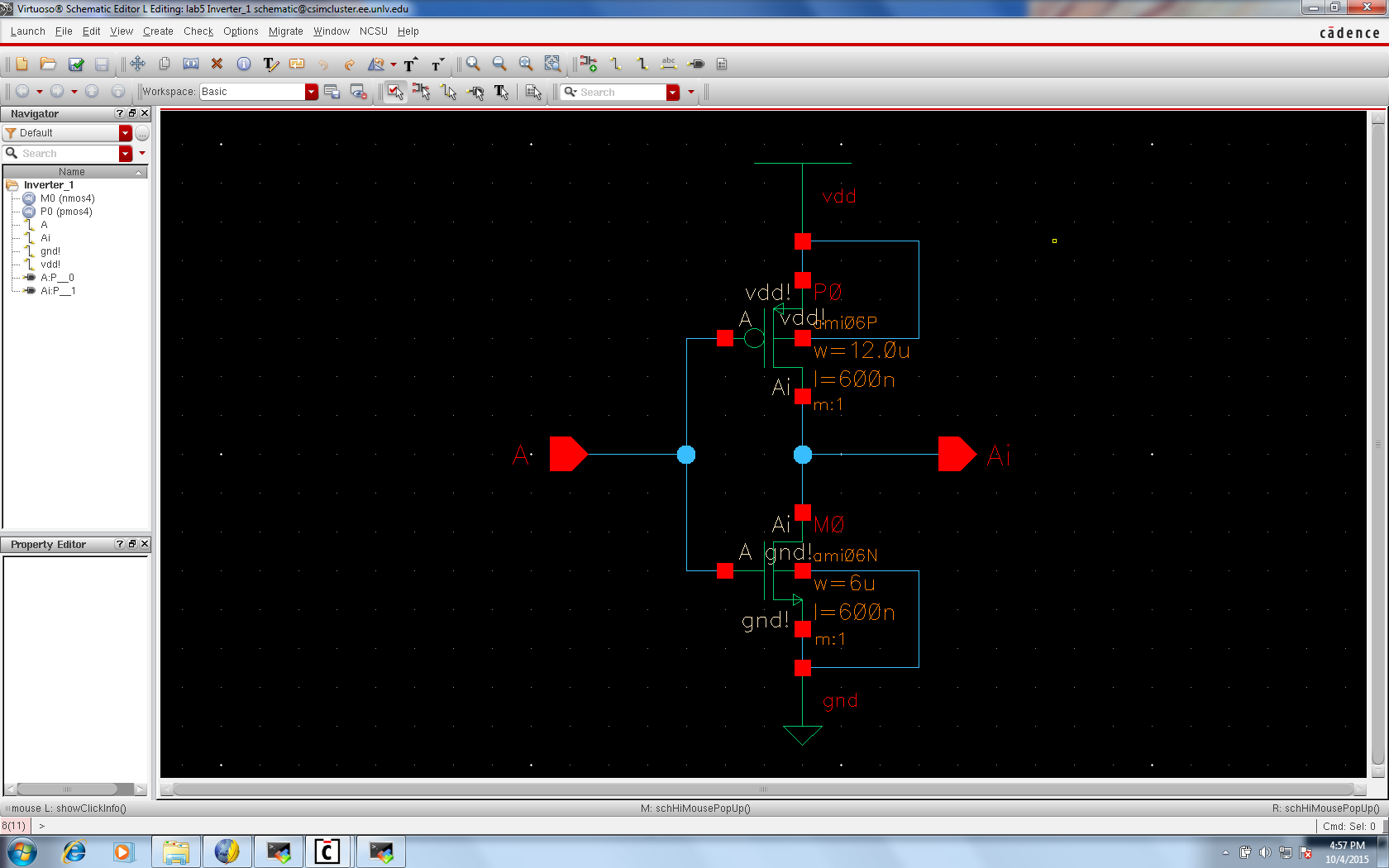
The following is the 12u/6u Inverter Device Schematic
The following is the 12u/6u Inverter Device Layout with DRC Verification
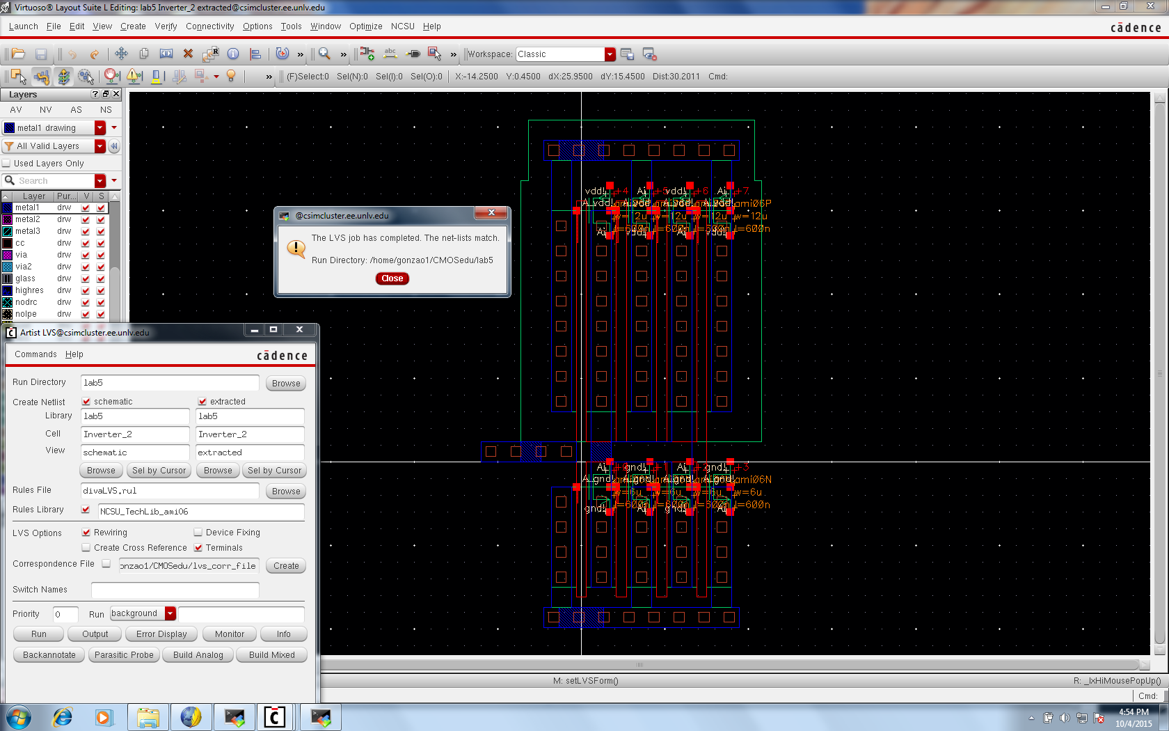
The following is the 12u/6u Inverter Device Extracted Layout with LVS Verification

The
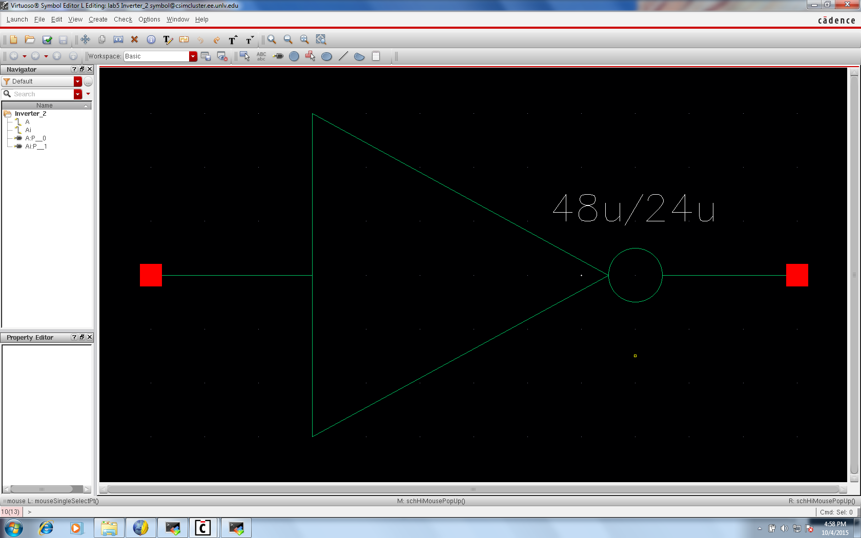
following is the 48u/24u Inverter Device Symbol
The following is the 48u/24u Inverter Device Schematic

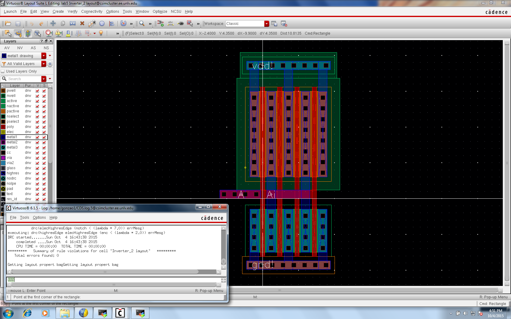
The following is the 48u/24u Inverter Device Layout with DRC Verification
The following is the 48u/24u Inverter Device Extracted Layout with LVS Verification
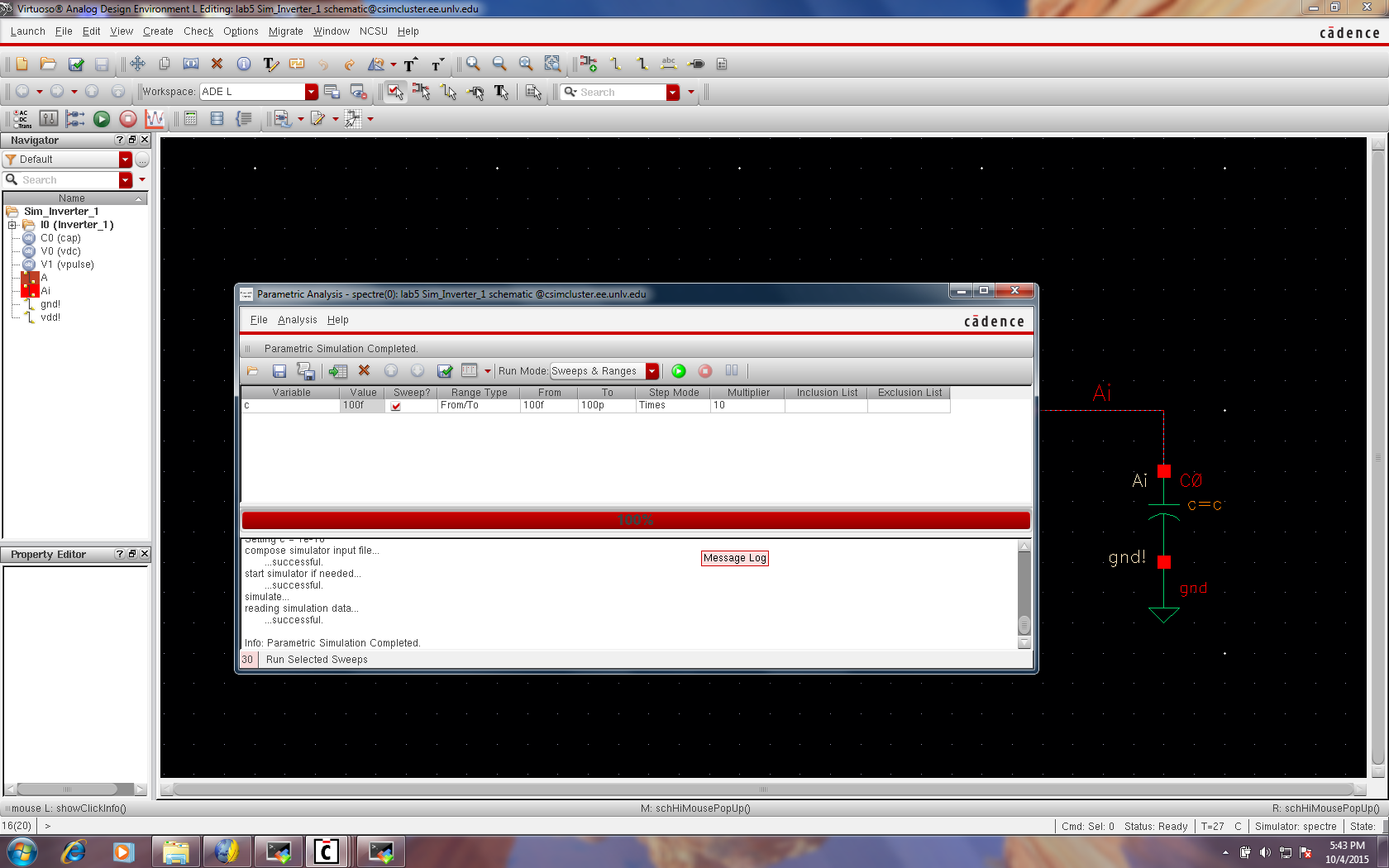
The following are the simulations for both the 12u/6u and 48u/24u inverters driving a 100 fF, 1 pF, 10 pF, and 100 pF capacitive load.
Note: These simulations wer performed using the parametric analysis tool.
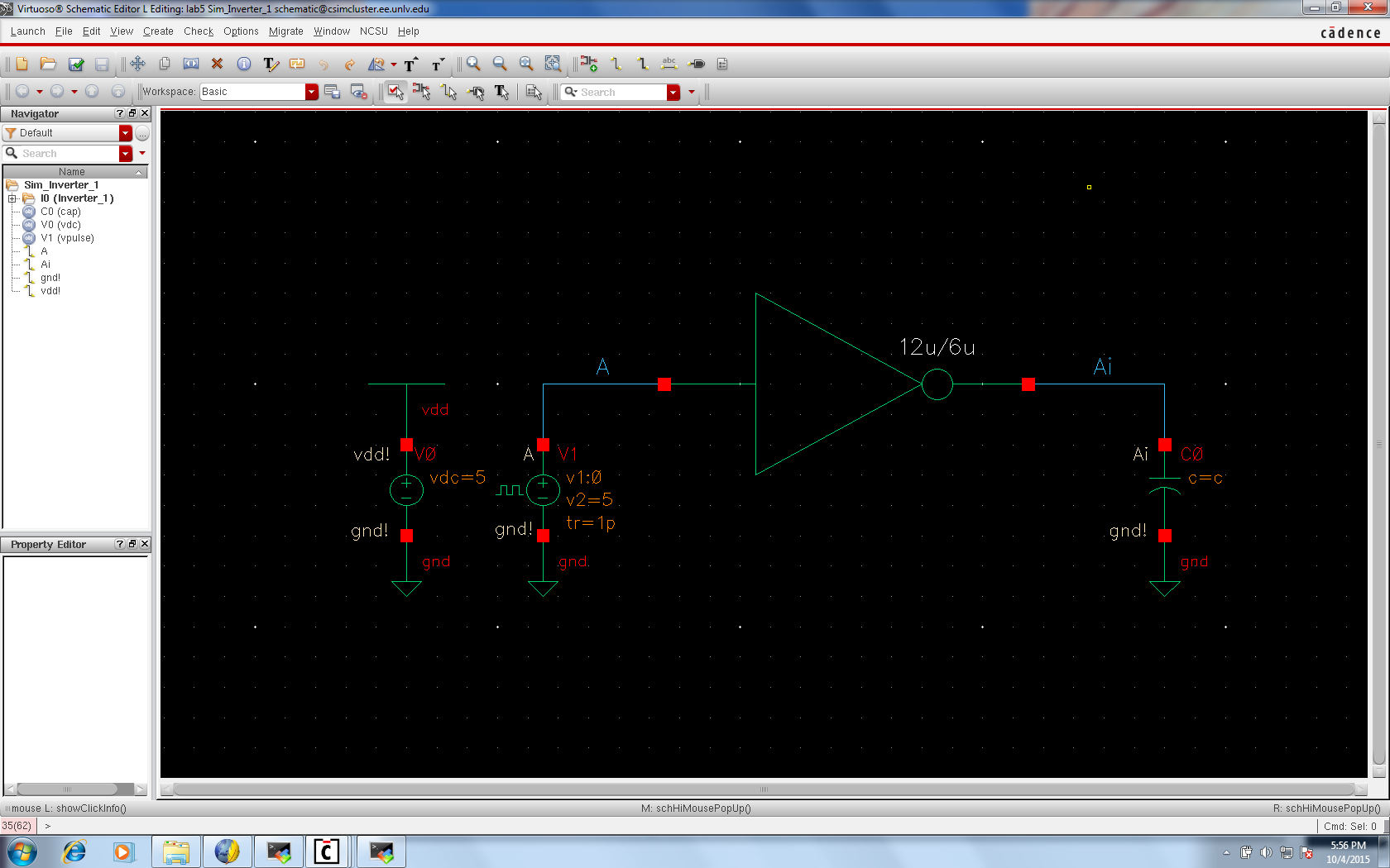
The following is the corresponding 12u/6u inverter device schematic..
The
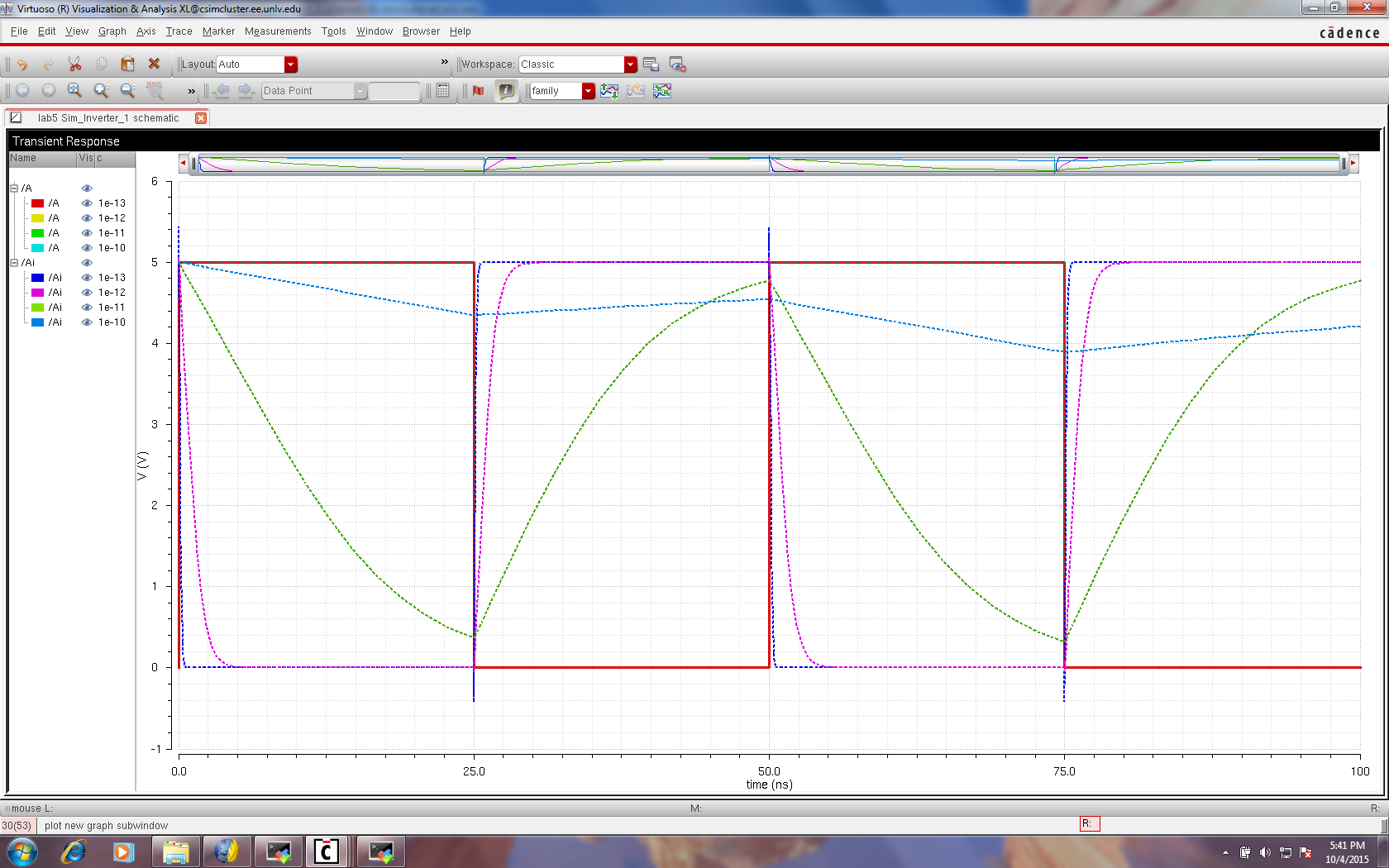
following is the corresponding 12u/6u inverter device simulation.
Note: As can be seen, with the larger capacitive loads, the RC time constant is also larger. The R is specific to the MOSFET W/L dimensions.
(UltraSim)

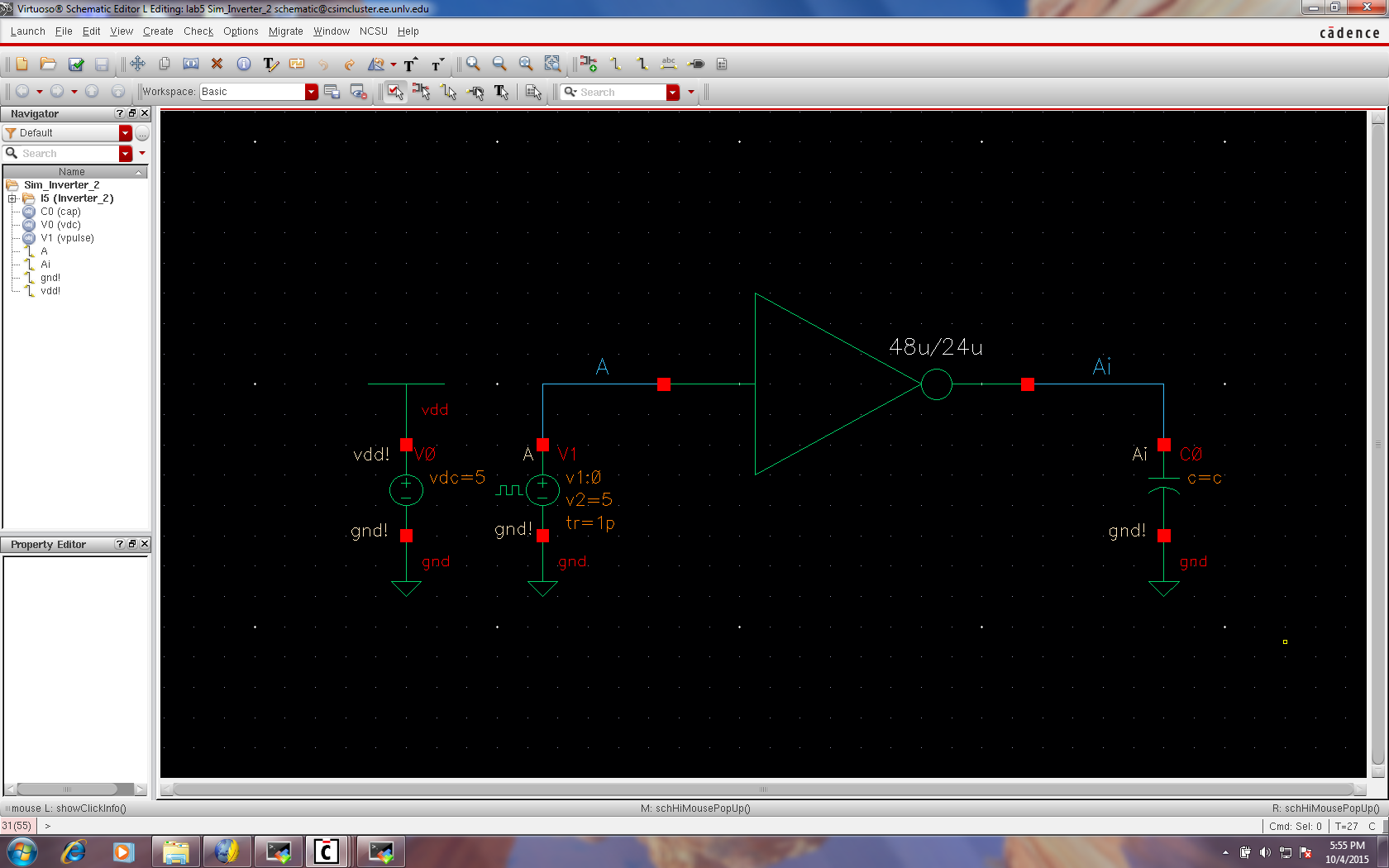
The following is the 48u/24u inverter device schematic.
The following is the corresponding 48u/24u inverter device simulation.
Note: As can be seen, with the larger capacitive loads, the RC time constant is also larger. The R is specific to the MOSFET W/L dimensions.

(UltraSim)
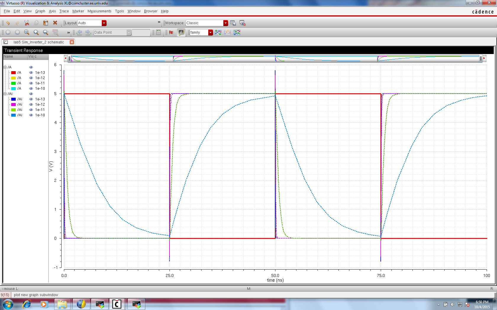
Note: Because the 48u/24u MOSFET has a smaller R than the 12u/6u MOSFET,
the larger inverter is better suited for the larger capacitive load as
the charge and discharce time constant is quicker than with the smaller
dimension device.
The following is a link to the zipped design files and directory
The webpage and design directory was backed-up during the pre-lab portion of the lab.
Lab 5 served as a means to design, layout, and simulate a CMOS inverter in the ON's C5 process.