Lab 4 - EE 421L: Digital Integrated Circuit
Design Laboratory
IV
characteristics and layout of NMOS and PMOS devices in ON's C5 process
Lab Work
Post-Lab Scope
Below
are the pre-lab deliverables.
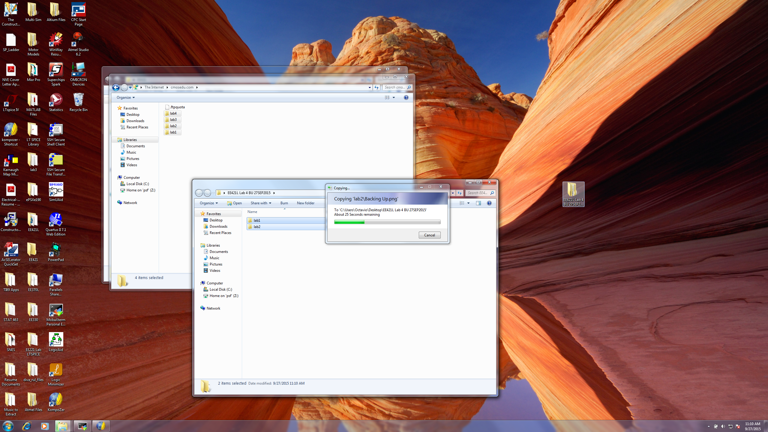
As can be seen, before starting, backing up all the work from the EE421 Lab and Course is required.
Saving the CMOSedu Directory Files to Folder EE421L Lab 4 BU 20SEP2015 on the Desktop
Emailing EE421L Lab 4 BU 27SEP2015 Zip to gonzao1@unlv.nevada.edu

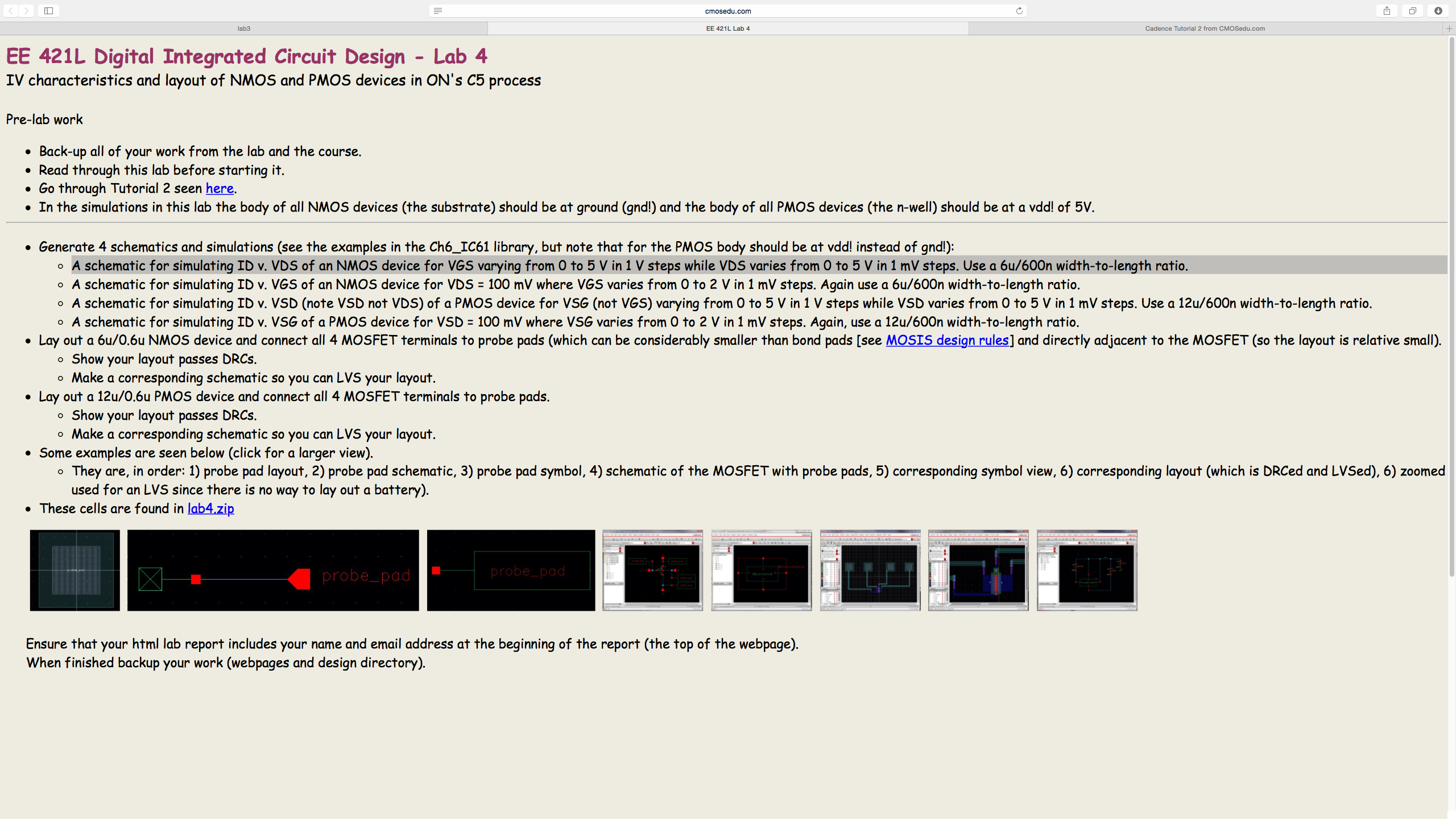
Below is a screenshot of reading through the Lab 4 requirements and scope prior to starting the assignment.
Tutorial 2
As can be seen below, Tutorial 2 has been completed. Note: LVS without errors.

Post-Lab:
Below are the post-lab deliverables.
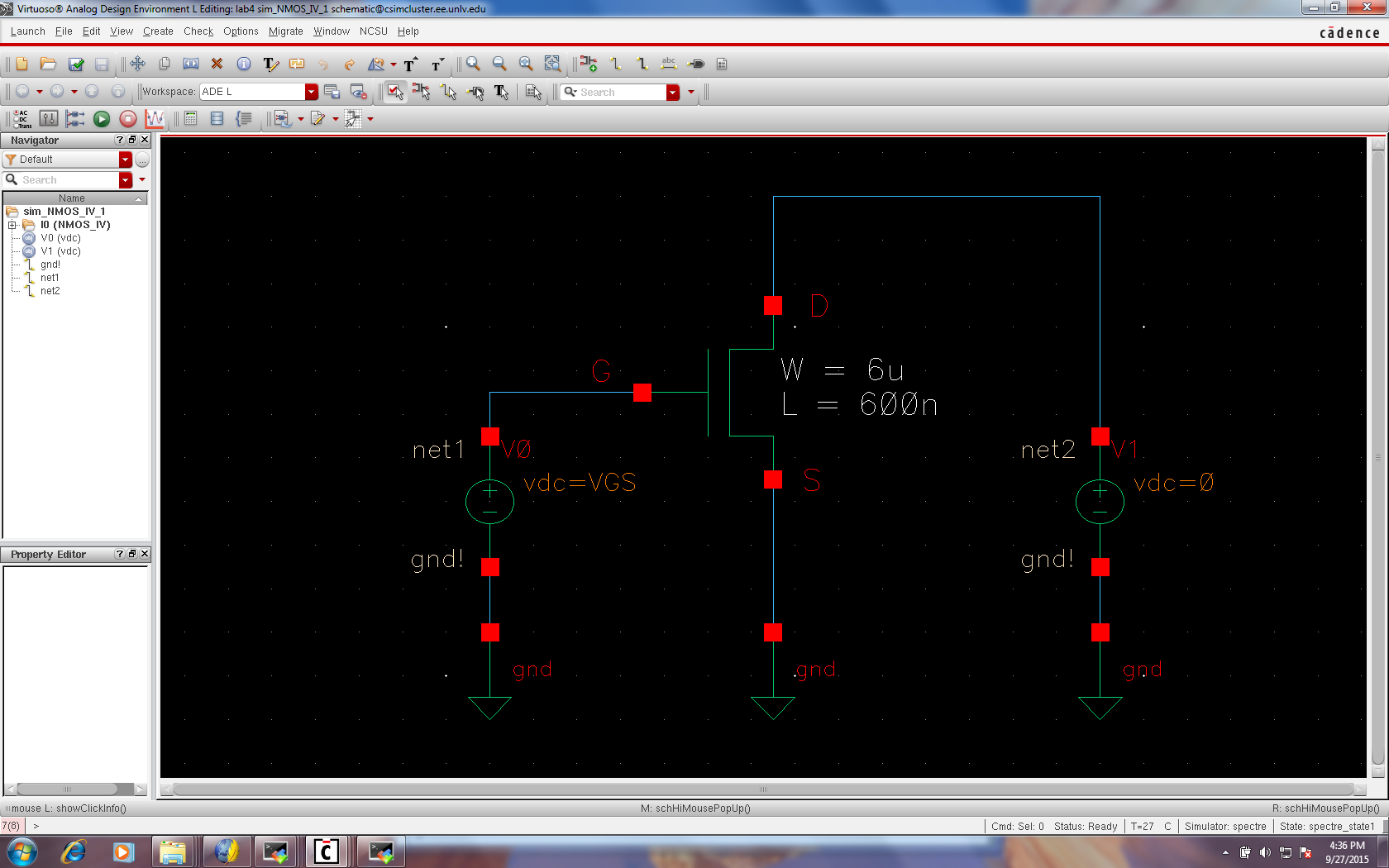
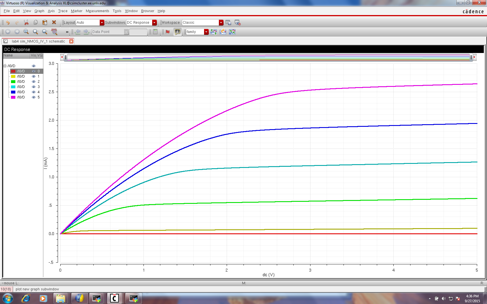
The following is the schematic for simulating ID vs. VDS of an NMOS device for varying VGS.
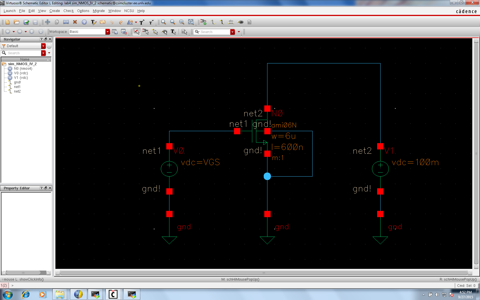
The following is the schematic for simulating ID vs. VGS of an NMOS device for varying VGS.

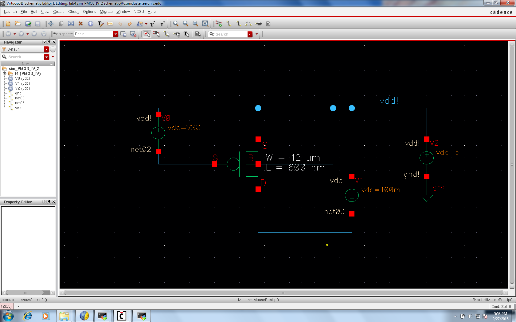
The following is the schematic for simulating ID vs. VSD of a PMOS device for varying VSG.
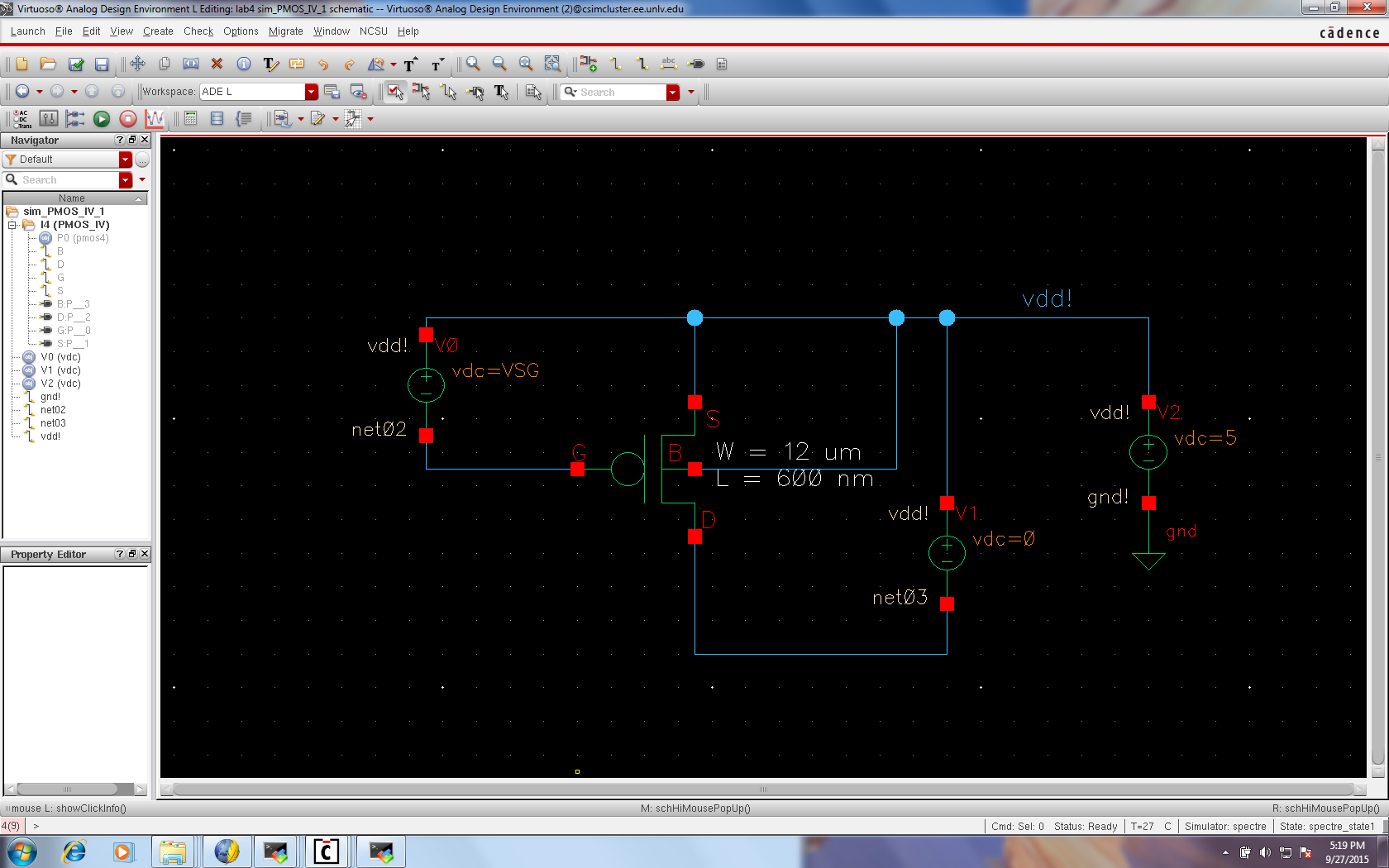
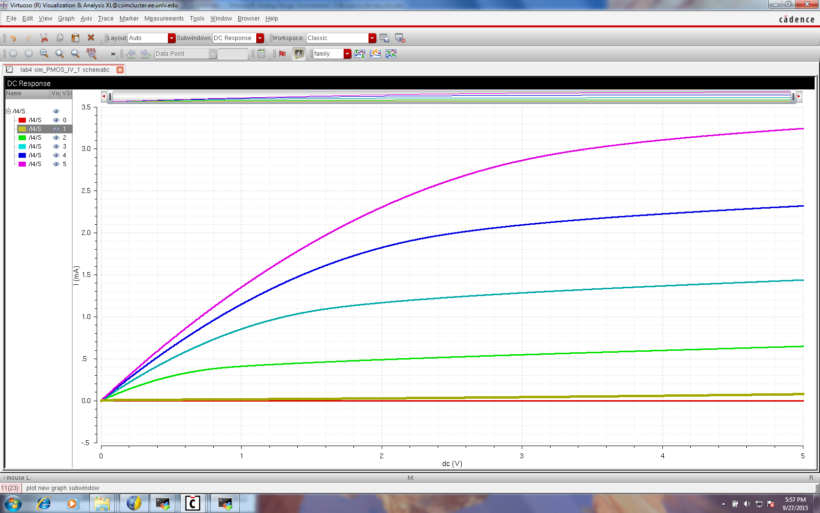
The following is the schematic for simulating ID vs. VSD of a PMOS device for varying VSG.

The following is a layout for the 6u/0.6u NMOS device connected to probe pads
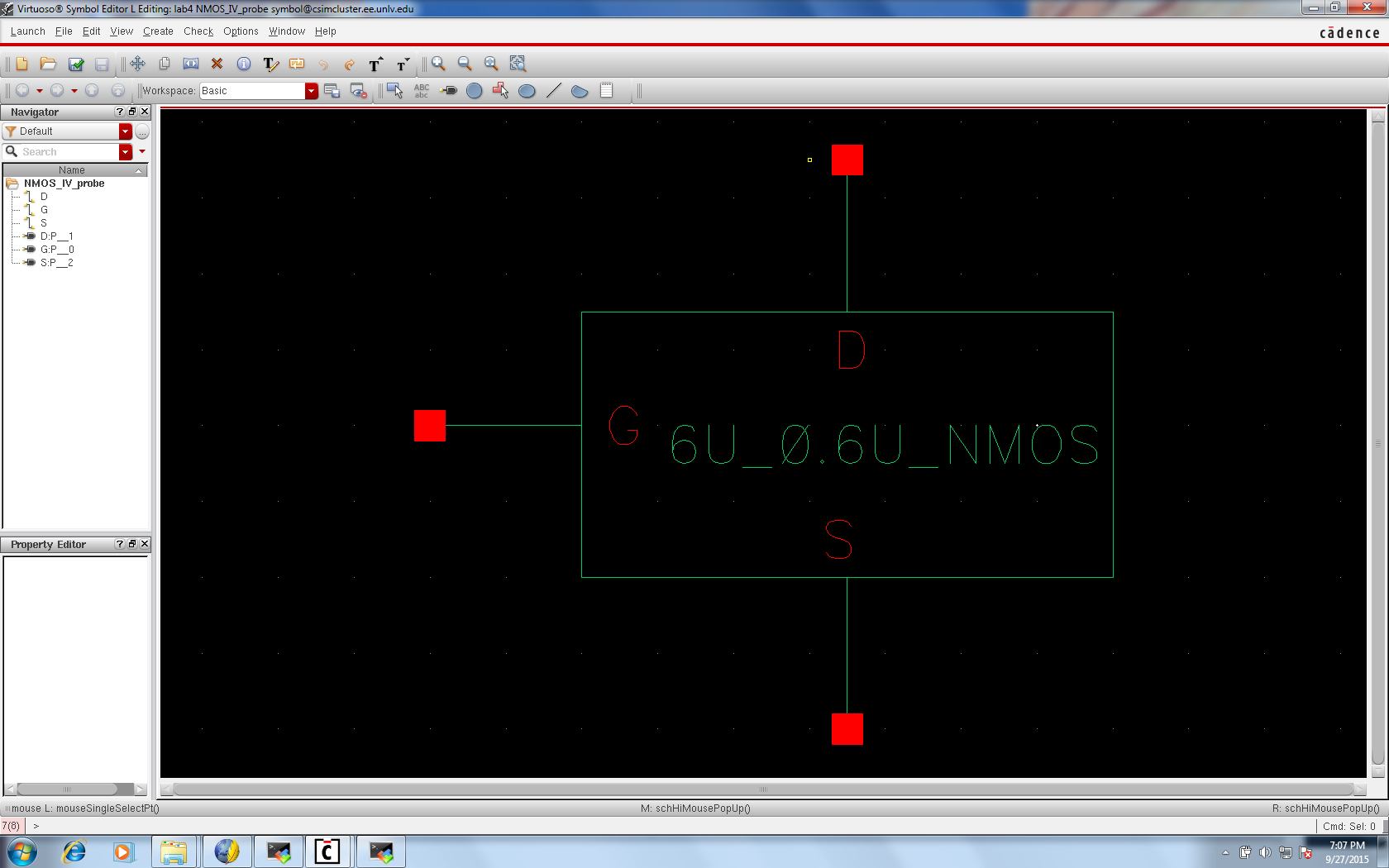
The following is the NMOS Device Layout Symbol
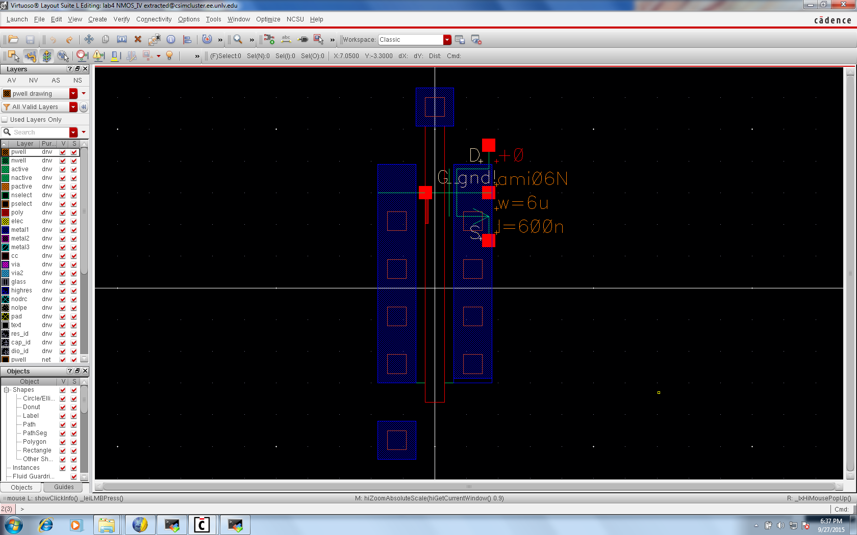
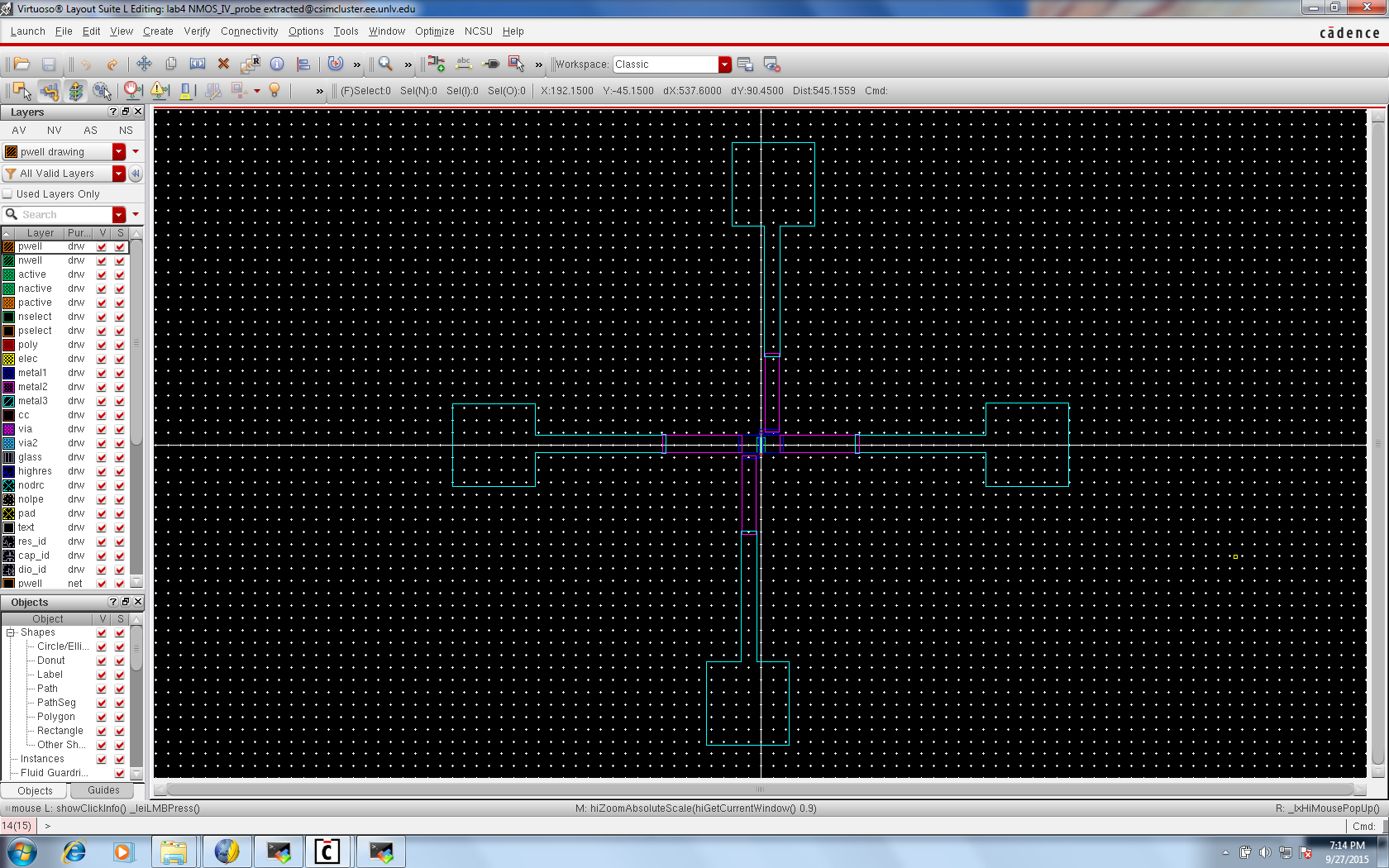
The following is the NMOS Device Layout

The following is the NMOS Device Extracted Layout
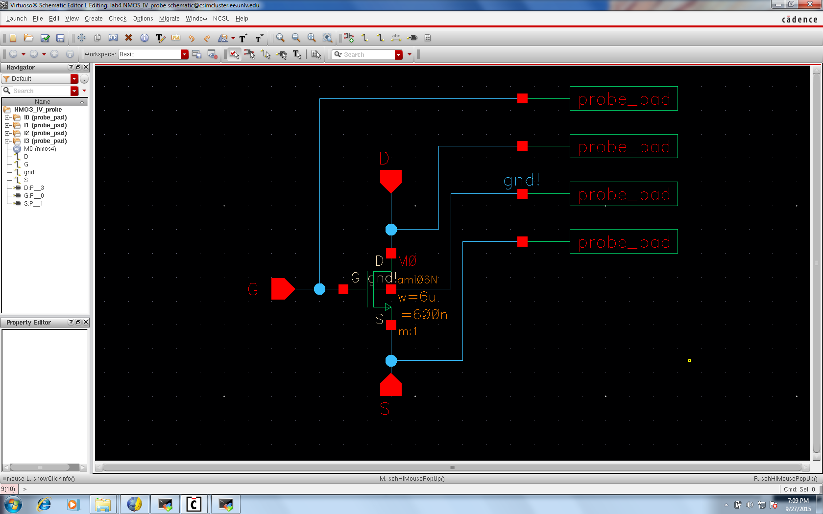
The following is the NMOS Device Connected Pad Layout

The following is the NMOS Device Connected Pad Extracted Layout
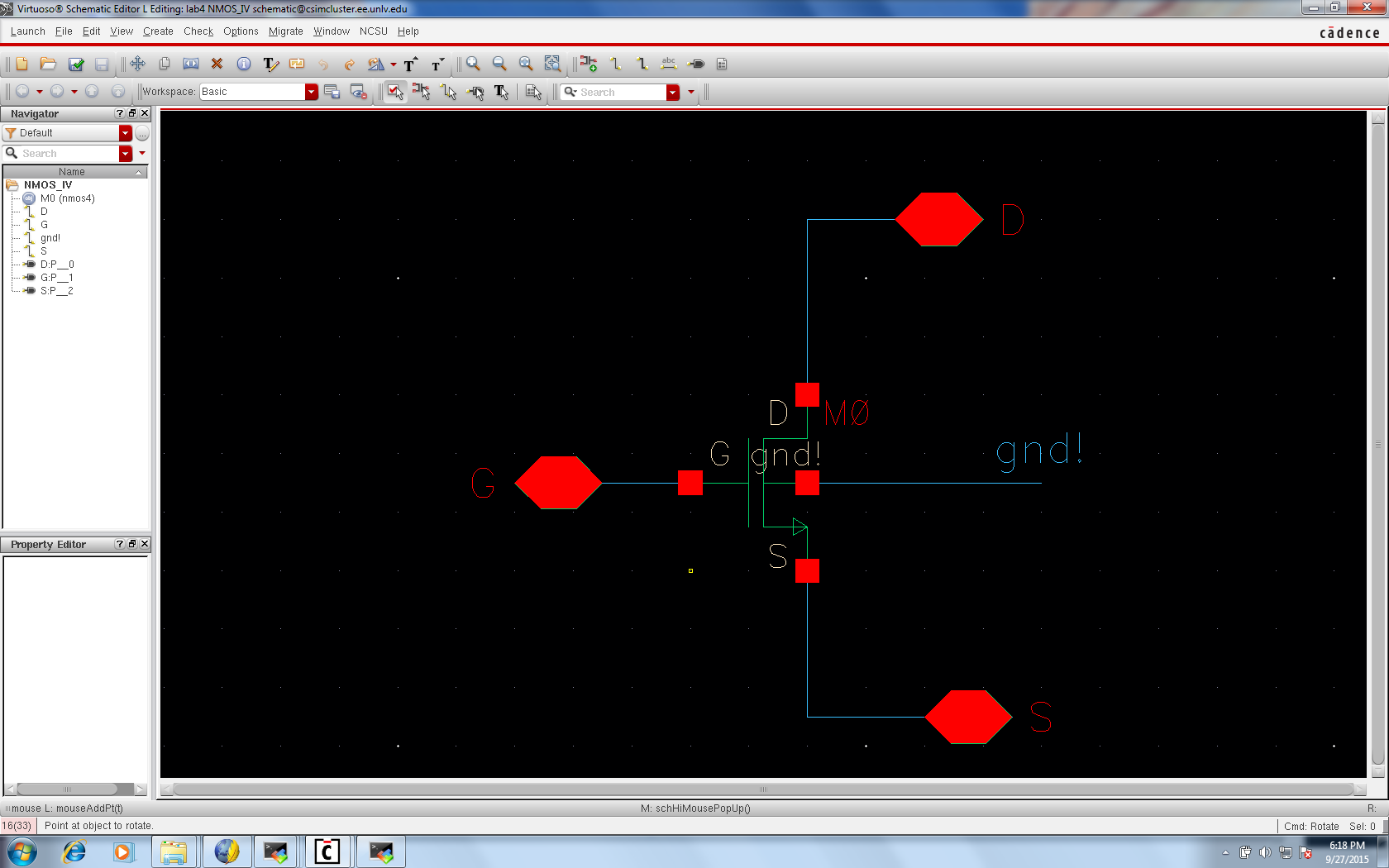
The following is the NMOS Device Connected Pad Schematic
The following is the NMOS Device Schematic
The following is the NMOS Device Symbol

The following is verification that the NMOS Device Connected Pad Layout DRC's correctly

The following is verification that the NMOS Device Connected Pad Layout Simulation Schematic LVS's correctly

The
following is a layout for the 12u/0.6u PMOS device connected to probe pads
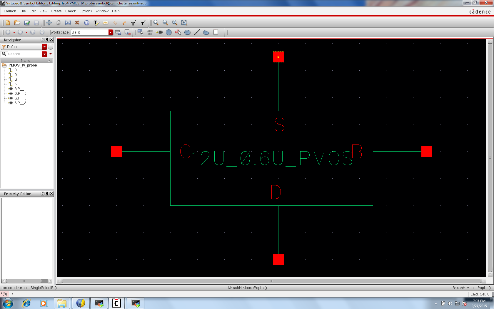
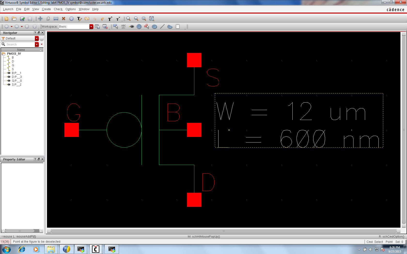
The following is the PMOS Device Layout Symbol
The following is the PMOS Device Layout

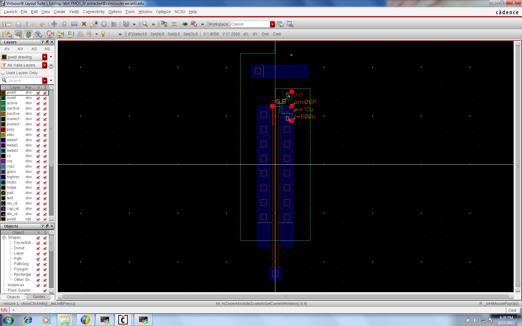
The following is the PMOS Device Extracted Layout
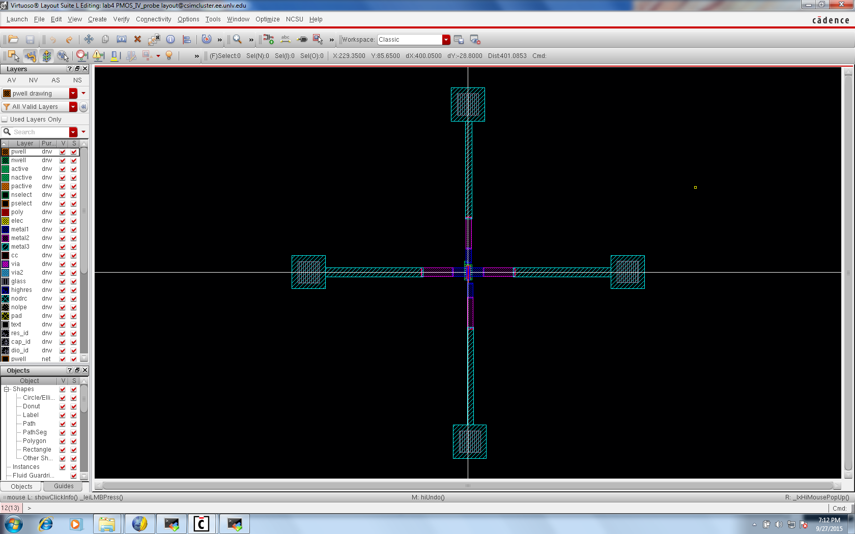
The following is the PMOS Device Connected Pad Layout
The following is the PMOS Device Connected Pad Extracted Layout

The following is the PMOS Device Connected Pad Schematic

The following is the PMOS Device Schematic

The following is the PMOS Device Symbol
The following is verification that the PMOS Device Connected Pad Layout DRC's correctly

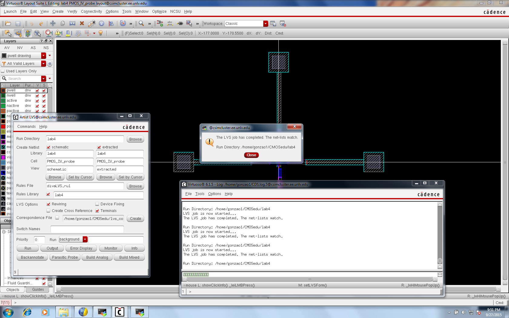
The following is verification that the PMOS Device Connected Pad Layout Simulation Schematic LVS's correctly
Lab 4 served as a means to understand the IV characteristics and layouts of NMOS and PMOS devices in the ON's C5 process.