Emailing EE421L Lab 3 BU 20SEP2015 Zip to gonzao1@unlv.nevada.edu
Lab 3 - EE 421L: Digital Integrated Circuit
Design Laboratory
Lab Work
Post-Lab Scope
Below
are the pre-lab deliverables.
As can be seen, before starting, backing up all the work from the EE421 Lab and Course is required.
Saving the CMOSedu Directory Files to Folder EE421L Lab 3 BU 20SEP2015 on the Desktop

Finish Tutorial 1
As can be seen below, Tutorial 1 has been completed. Note: LVS without errors.

Post-Lab:
Below are the post-lab deliverables.
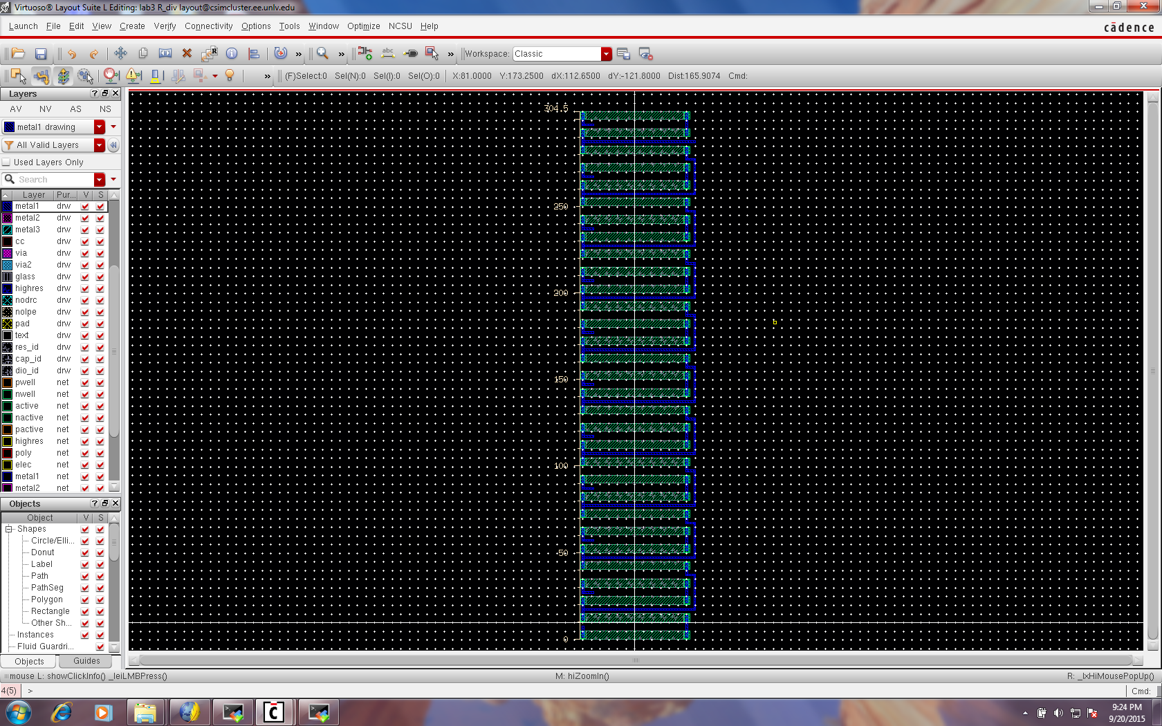
The following screenshots show how the DAC 10k n-well Resistors were layed-out.
Each resistor in the DAC is laid out in parallel having the same x-position but varying y-positions.
Note: The resistors are stacked and modular.
Each n-well resistor and metal 1 contact is checked against the process design rules to ensure that the spacing is within the specified tolerances.
Note: The DRC shows no errors.

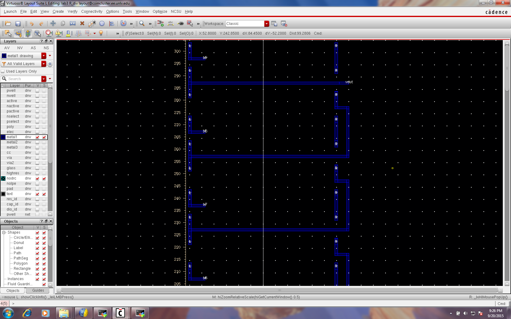
The
following layout view shows that all input and output pins are located on the metal 1 layer.
The metal1 layer and NV view were selected to verfy that all metal1 and pin connections are located on the correct layer.
The
following is a brief discussion on how to select the width and length
of the resistor by referencing the process information from MOSIS.
Recall the following C5 process Constraints:
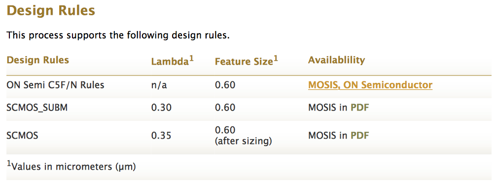
Lambda: 300nm
Minimum n-well width: 12*Lambda = 3.6 microns
Sheet resistance of an n-well: 800 Ohms/square
Also recall resistance equation: R = (p*L/A) = (p*L/(t*W)) = (R/sq)*(L/W)
To select the dimesions for a 10k n-well resistor, let the width W = 4.5um
Therefore.....
R = (R/sq)*(L/W) = (800 Ohms/sq)*(L/4.5um)
Solving for L yields --------> L = 56.25um
The n-well resistor must have a length of L = 56.25um
Because
the grid spacing is set to 0.15 microns, the L and W dimesnions will
need to be rounded up or down to the nearest whole number.
Measurement of Width and Length for 10k n-well Resistor
The
following is a brief discuss on how the width and length of the n-well resistors are measured.
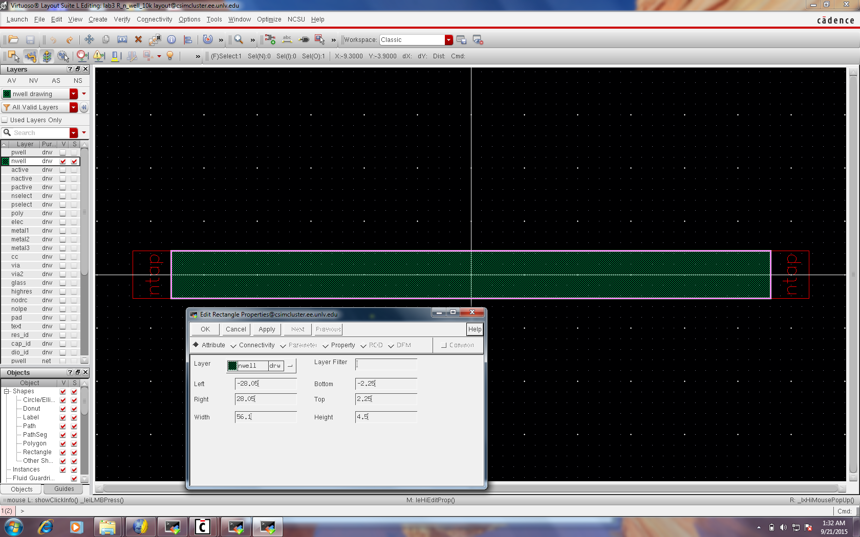
One method of measuring the width and length of the n-well resistor is to open the n-well rectrangle properties box.
Here the current X and Y rectangle layout dimensions are shown below. Note: These dimensions may be manually specified.
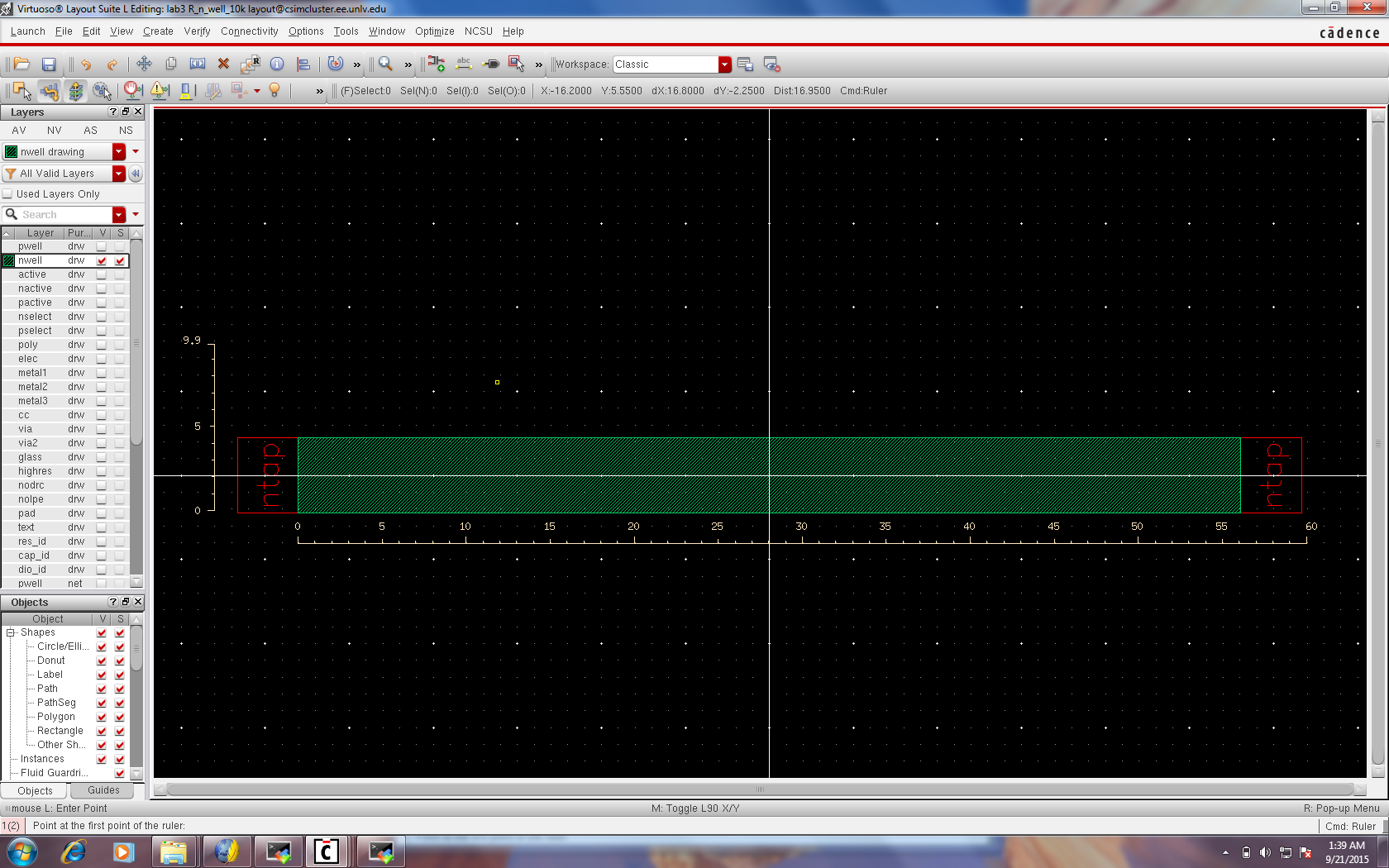
Another method of measuring the width and length of the n-well resistor is to use the ruler tool as shown below.
This can be set up using k and Shift-k to remove the ruler guides.
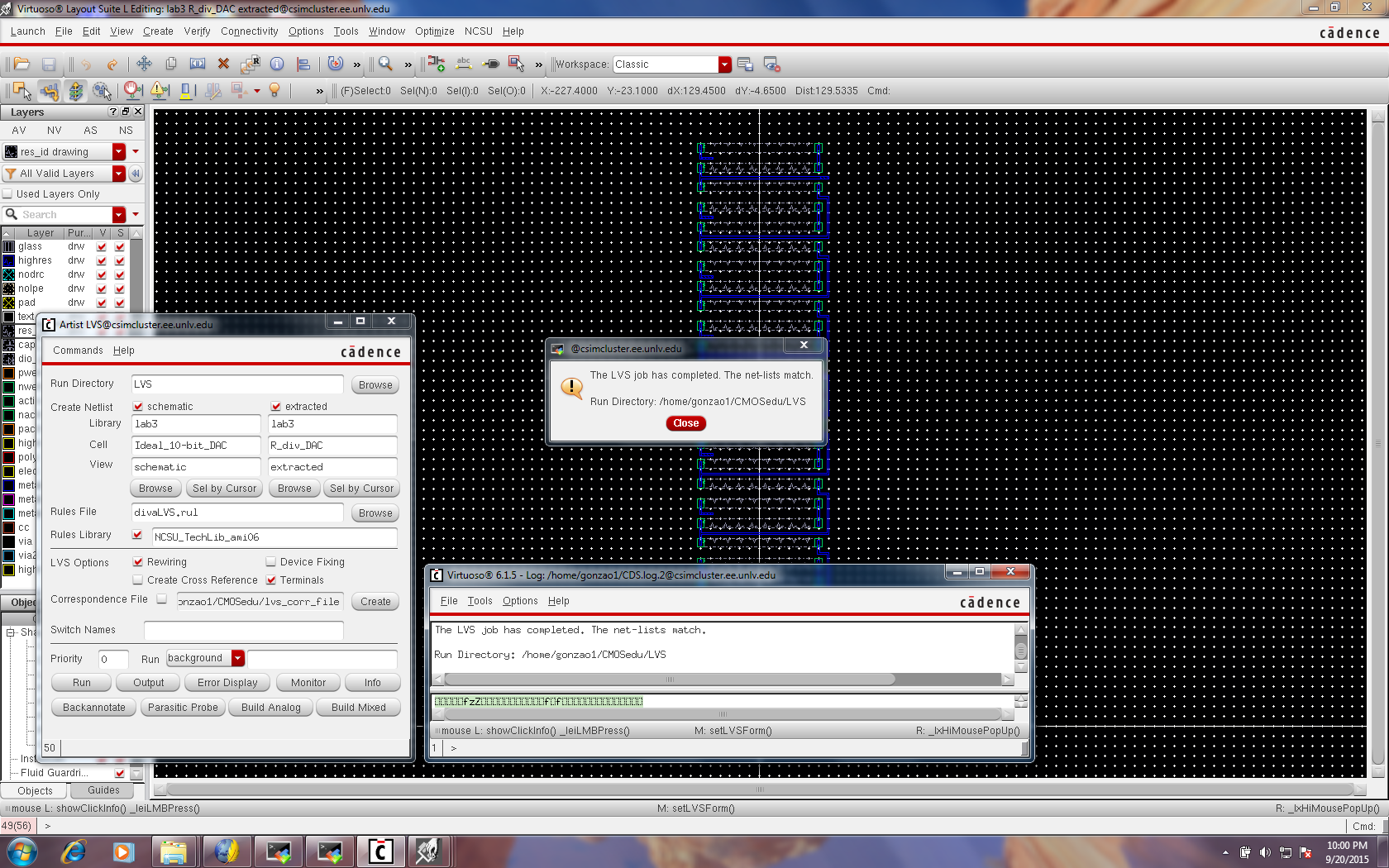
The following are screenshots of the DRC and LVS extracted layout design verifications.
DRC extracted layout design verifications. Note: No errors.

LVS extracted layout design verifications. Note: Net List Matched, no errors.
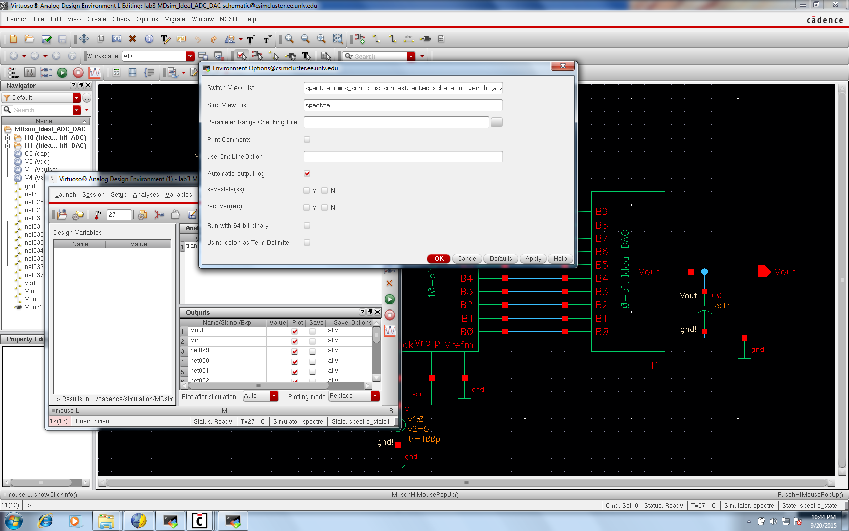
The following are screenshots of the extracted layout design simulations.
Schematic utilizing n-well layout.

Setting up the environment to run extracted schematic
Simulation Plot utilizing n-well layout.

The following is a link to the zipped design files and directory
Lab 3 has served as a
means to design the layout of a 10-bit digital-to-analog converter
(DAC) as well as DRC and LVS it to an existing 10-bit DAC schematic.