
Lab 2 - EE 421L: Digital Integrated Circuit Design Laboratory
Design of a 10-bit digital-to-analog converter (DAC)
Lab Work
Post-Lab Scope
Below are the pre-lab deliverables.
As can be seen, before starting, backing up all the work from the EE421 Lab and Course is required.
Below is a screenshot of reading through the Lab 2 requirements and scope prior to starting the assignment.

ADC/DAC Voltage Relationships
The voltage Vin, Vout, and B[9:0] are related by:
Vin is the analog input to the ADC, the nature of this signal is "time-continuous" and "infinite-valued", which means it continuous on the inteval [Vin, -Vin].
Vin is fed to the input of the ADC, where it is compared against a reference voltage
divider network. An arangement of comparators tied between this and Vin
switch on/off according to the different values that Vin takes on. By
this process, Vin's states are sampled into a Decoder element.
The output of the decoder becomes a digitized representation of Vin
designated as signal B.
B[9:0] is the digitized representation of Vin, it is said to be "discrete-time" and "quantized". In this lab B is a 10-bit representation of Vin which means it encodes with a resolution of:
2^n = 2^(10) = 1024 bits; where n is a 10 bit word
B is then fed to the input of the DAC, which consists of a resistive ladder network and trasistor switching scheme. The switching, based on the values of B[9:0], reconfigues the ladder network topology onto two separate busses. As a result, the voltage signal on these two busses varies in a discrete analog manner. Lastly, the busses are connected to the Vp and Vm inputs of an opamp for amplification.
Vout is the analog output of the DAC, the nature of this signal is "time-discrete".
It is a representation of the digitized signal in analog form.
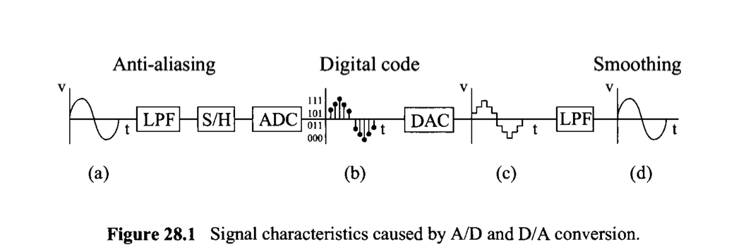
Taken from CMOS 3rd Edition
The following is a brief prelab narrative listing the steps. (Click on thimbnail for larger view)
P1: Download lab2.zip to your desktop.

P2: Upload the zip file to the design directory on the same server that is running Cadence.

P3: Unzip the directory and add, to the cds.lib in the design directory, the statement:
DEFINE lab2 $HOME/CMOSedu/lab2
(MODIFIED)

P4: Use the Library Manager and navigate to the lab2 Library.

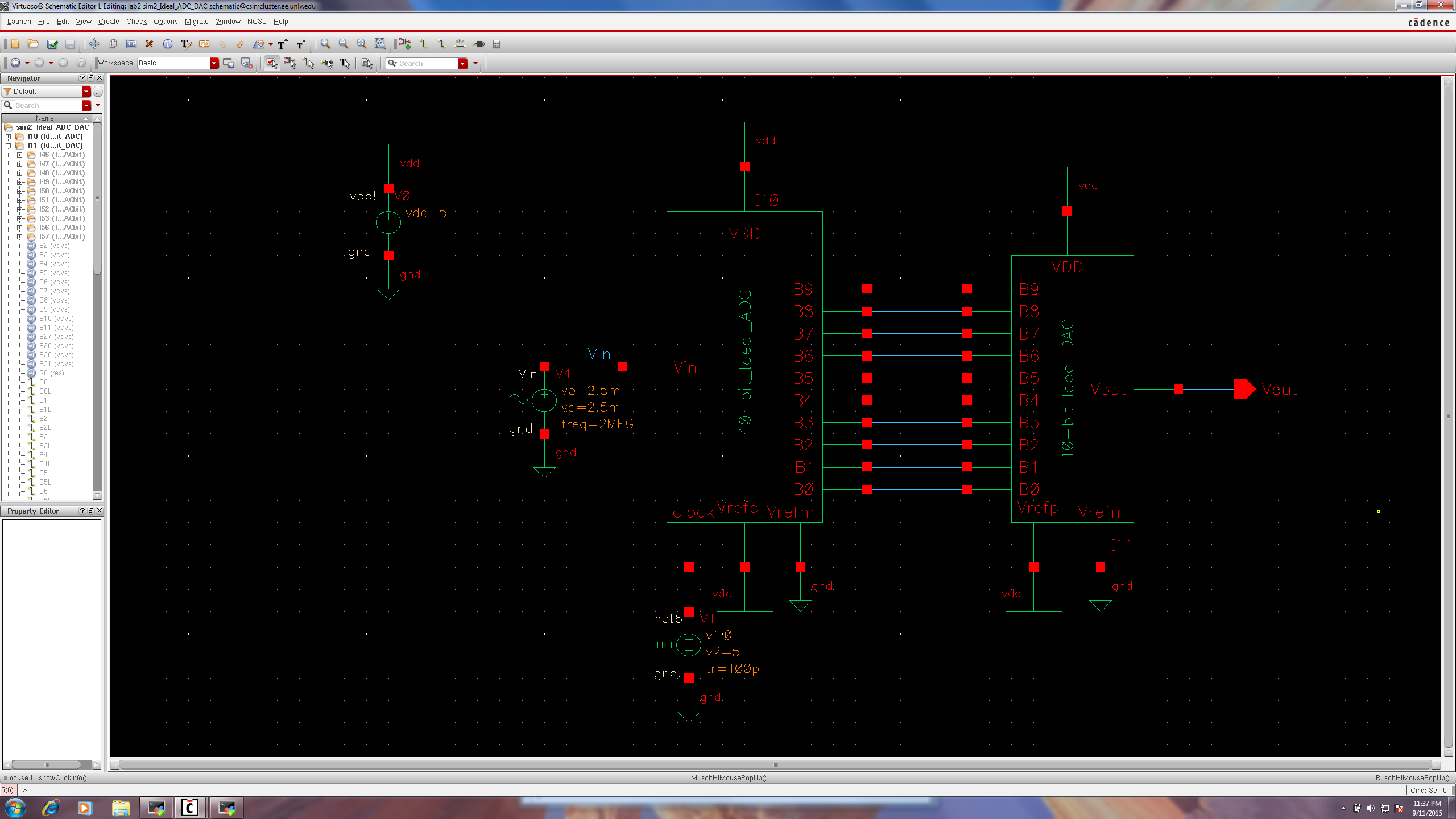
P5: Open the schematic view of the cell sim_Ideal_ADC_DAC.

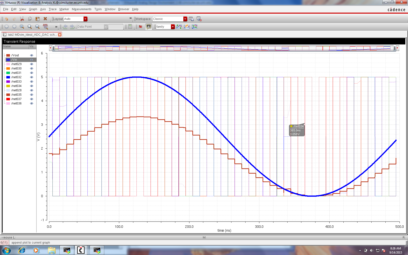
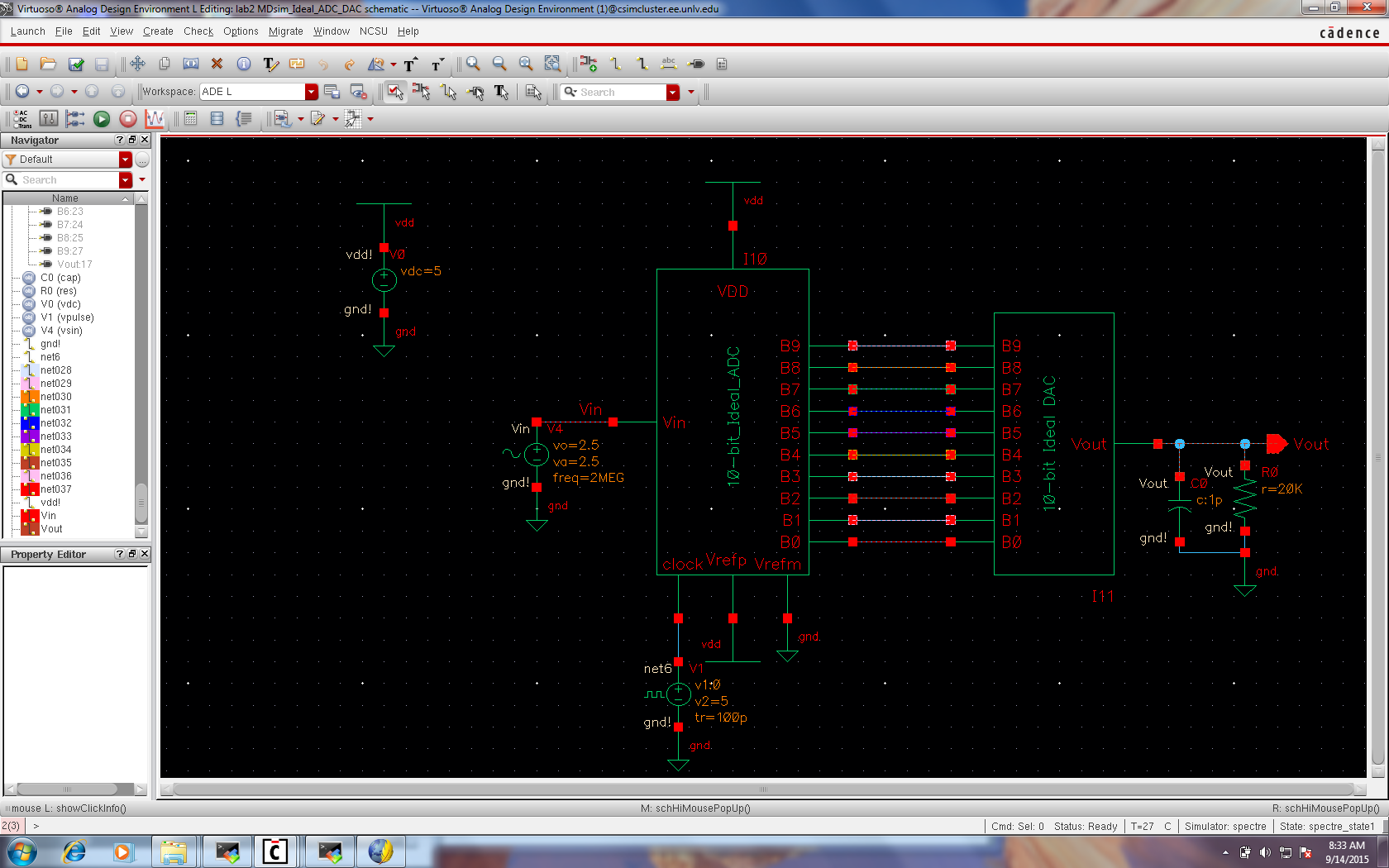
The following is the prelab simulation results for the ADC/DAC.

Schematic View
The
simulation was first ran "as is" to match the one in the prelab. Once
this was accomplished the trace widths and trace style were changed for
better visibility, along with plotting the digital waveform present on
the B[9:0] lines. This was done to see the process from Vin to B[9:0] to Vout.

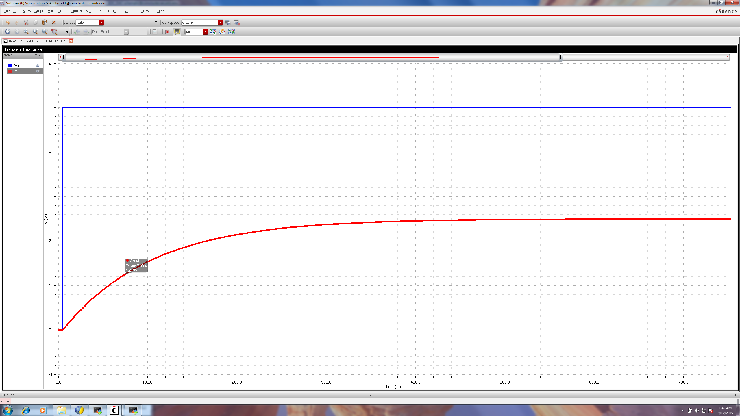
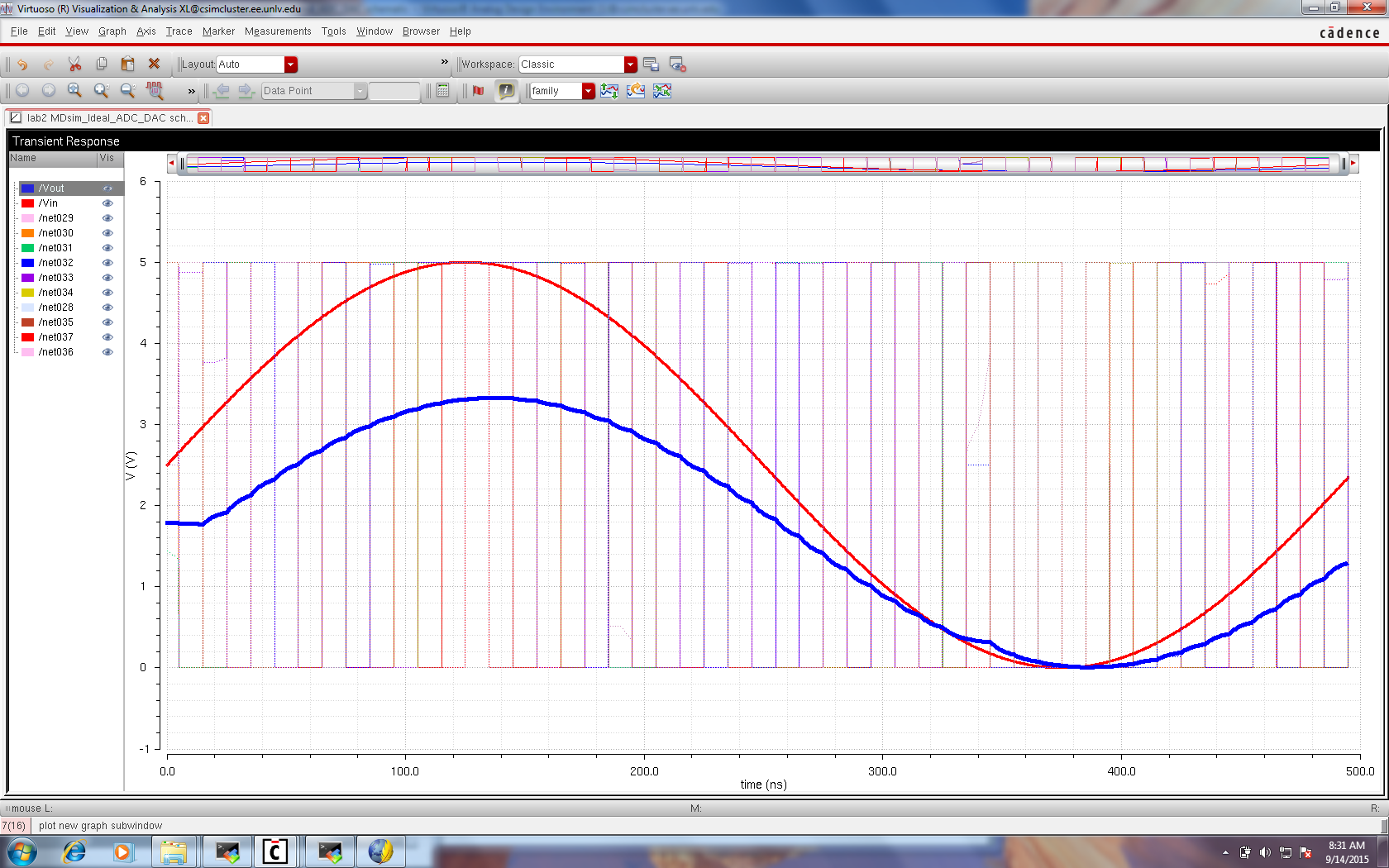
Vin, Vout, and B[9:0]
The
simulation was further modified from Vin to Vin' by changing the V4 source parameters (Vin).
| Parameter | Vin |
Vin' |
| Offset Voltage |
2.5V |
2.0V |
| Amplitude |
2.5V |
5.0V |
| Frequency |
2MHz |
1MHz |
The following simulation results are different from the prelab.
Due to an analog Vin that exceeds the encoding range, the output waveform is pegged and therefore appears as clipping.

The following is a brief discussion on how to determine the Least Significant Bit (LSB) for the ADC.
Recall: Since the ADC must quantize and infinite-valued analog signal, the following expression must be satisfied:
Q = Number of Quantization Levels = 2^n = 2^(10) = 1024 values
which corresponds to the 10 bit digital code.
Recall: The calculation for determining the volatge corresponding to 1 LSB:
1 LSB = VRef/(2^n); where 2^n = Q
1 LSB = (5V)/(1024 Bits) = 4.882813 mV/Bits
The
simulation was further modified from Vin to Vin" by changing the V4 source parameters (Vin).
| Parameter | Vin |
Vin' |
| Offset Voltage |
2.5V |
2.5V |
| Amplitude |
2.5V |
5mV |
| Frequency |
2MHz |
2MHz |
By
changing the input voltage to barely cross the LSB threshold, it can be
seen that only one quantized value is representing Vin and thus the
resultant Vout only has a resolution of 1 bit. This is because Vin is
set to only cross the corresponding voltage of 1 LSB.

Post-Lab:
Below are the post-lab deliverables.
The following is the 10-bit DAC design using an n-well R of 10k.


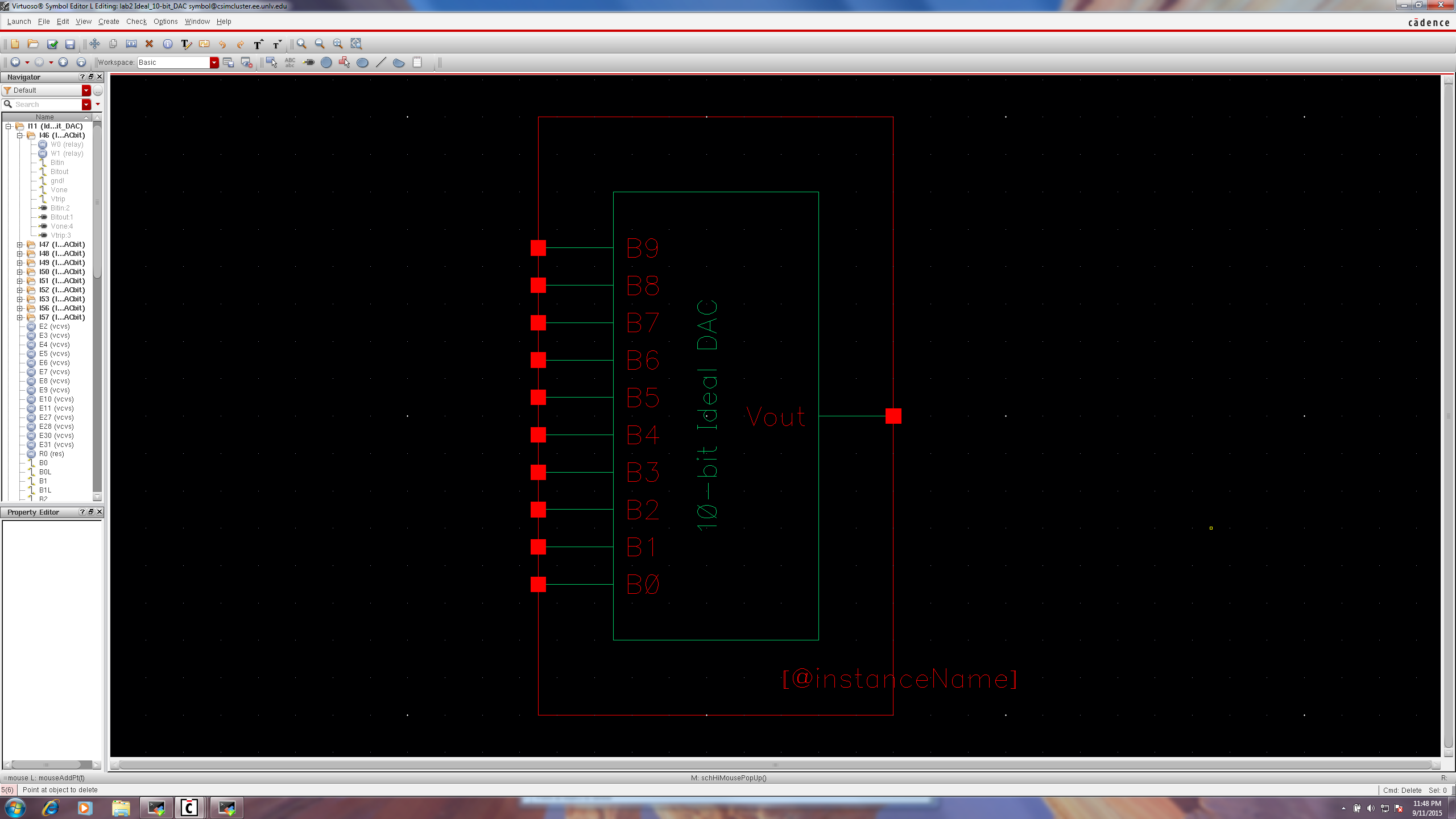
Opening the Re-named Simulation Schematic and modifying the DAC Symbol. (Demo obsolete Pins)
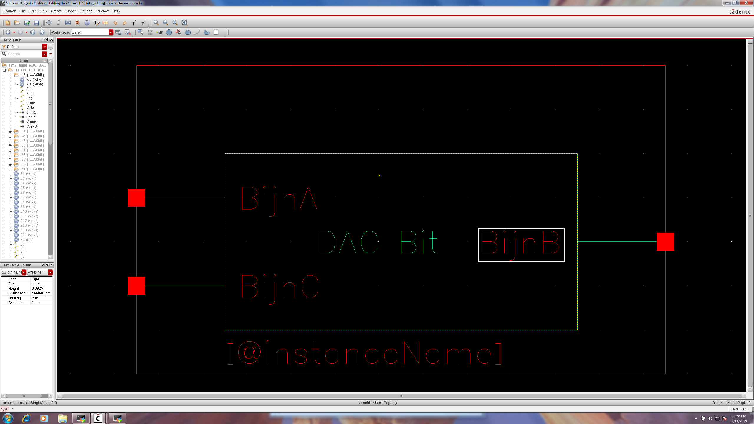
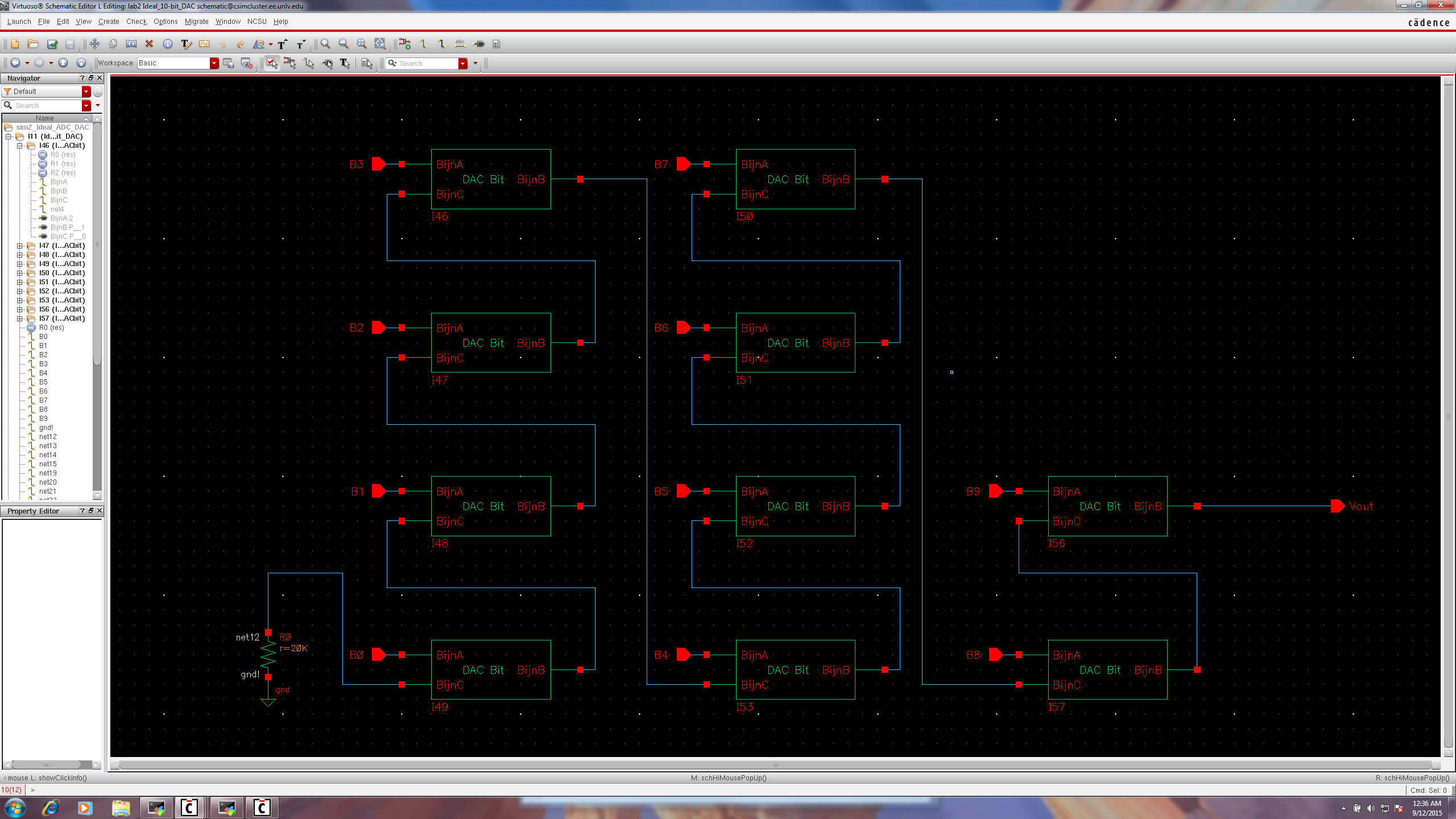
Editing the Bit Symbol and DAC Schematic.
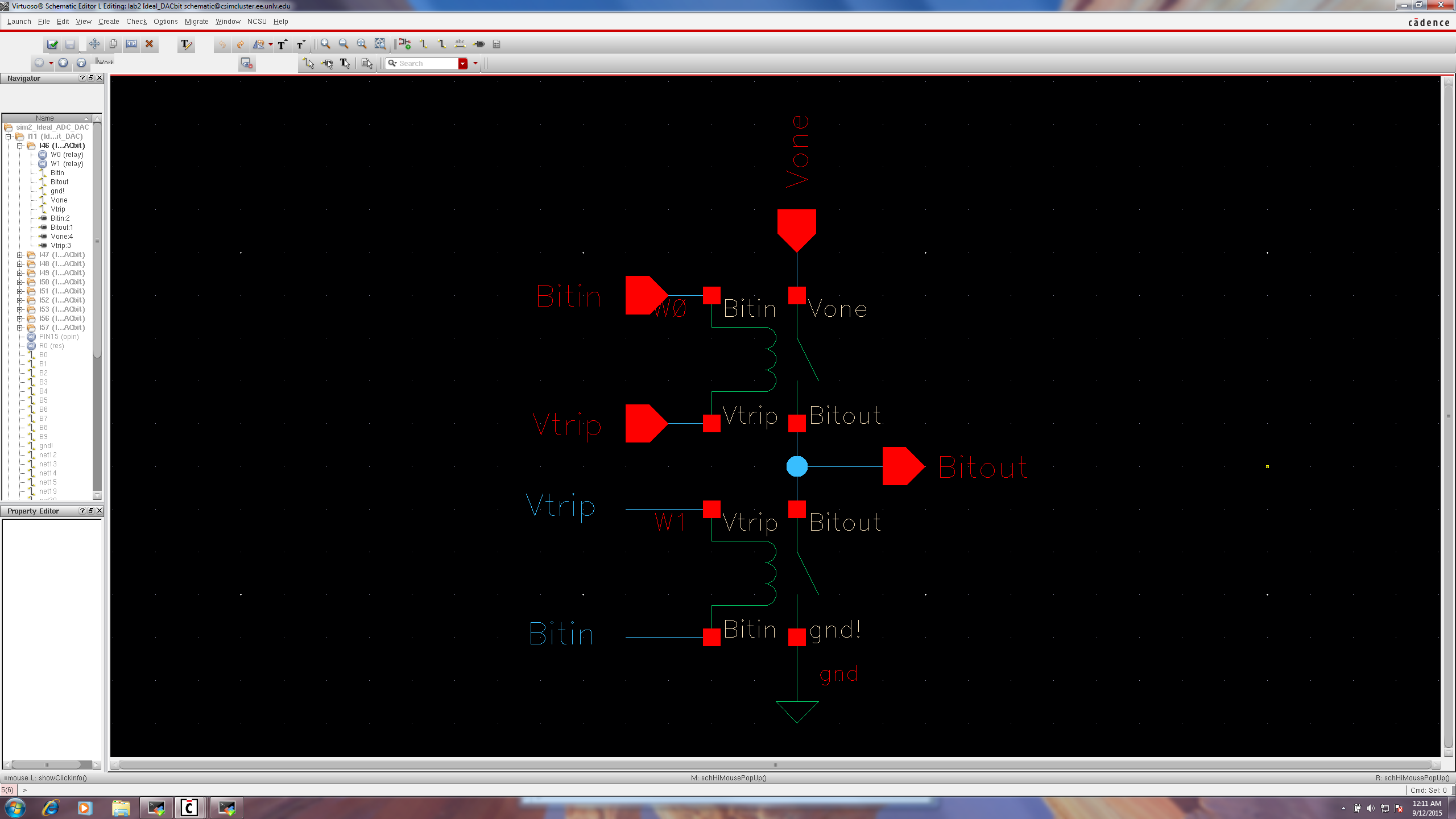
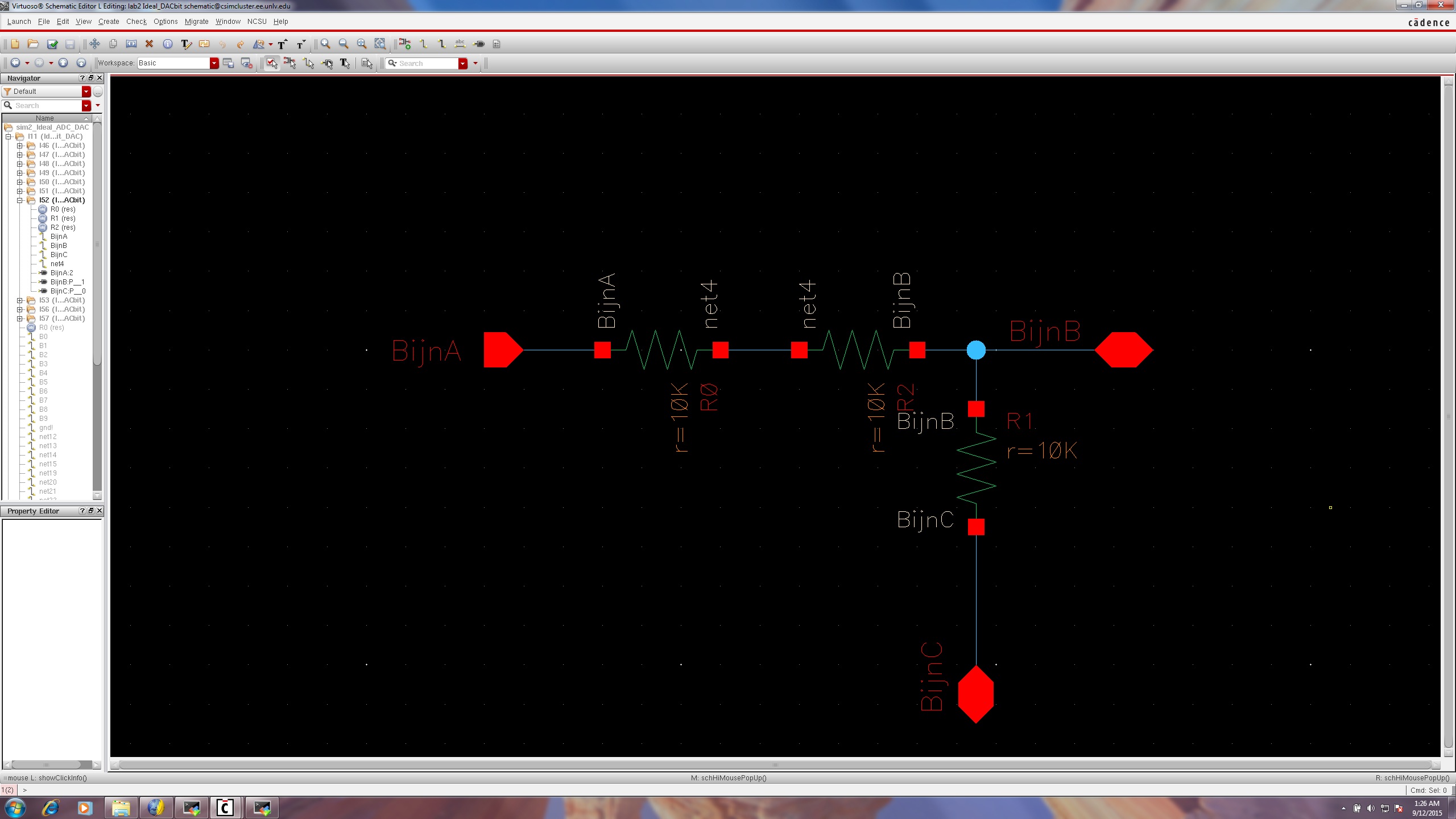
Modifying the Bit Schematic.
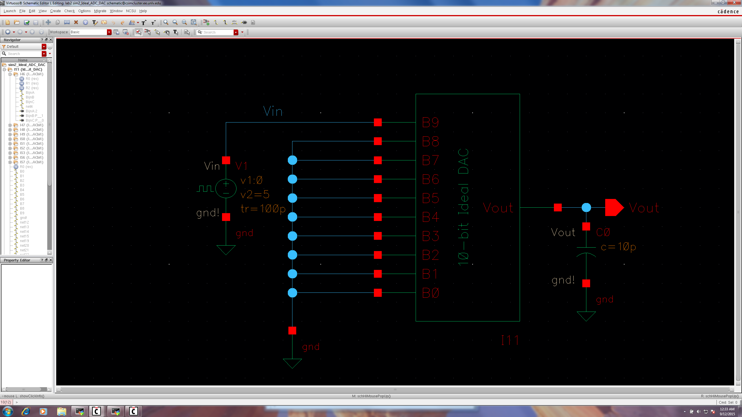

Modifying the Simulation Schematic
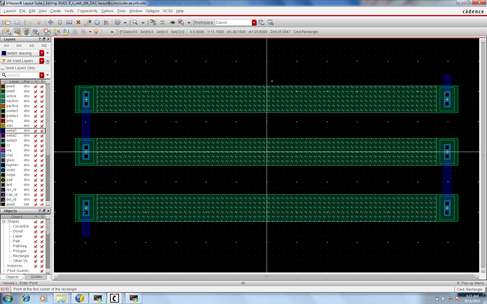
n-well Resistor 10k Ohms
The following is a method for determining the ouput resistance of the DAC.
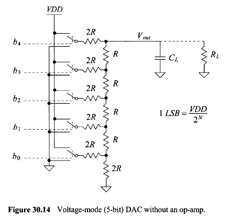
For the given topology in Figure 30.14, the DAC output resistance, can be calculated byThevenin Equivalence.
The resultant resistive ladder diagram impedance as seen from Vout is then expressed as:
Rout = ((((((((..................||2R)+R)||2R)+R)||2R)+R)||2R)+R)||2R
Which yeilds, for any value R in the same topology:
Rout = R
The following is a comparison between simulation results and hand calculations.
For the given topology in Figure 30.14, the DAC time delay, from b9 to bout with a 10pF capacitive loading can be calculated.
The time delay caculation will be performed in a similar manner to the DAC output resistance method presented above.
All pins are to be grounded except for b9, which will serve as the input to the time delay signal to be measured.
By the Thevenin Equivalence principle and series/parallel reduction, it is evident that:
Vout = Vin*(2R/(2R+2R)) = Vin*(1/2)
Since Vout must be (Vin/2) for this configuation of the topology, the output signal 50% points must correspond to:
Vout50% = (Vin/2)*(50%) = (Vin/4)
Consequently, this is where the time delay output signal will be measured up to.
Recall the distributed quantity RC transmission line model and Time Delay Calculation for Figure 2.22.
Td = 0.7*R*C*(L*(L+1)/2)
Where
R = 10k Ohms, C = 10pF, L=1
Thus the expected time delay is:
Td = 0.7*(10k)*(10pF) = 70nS

Simulation Time Delay. (NOTE: Offest)
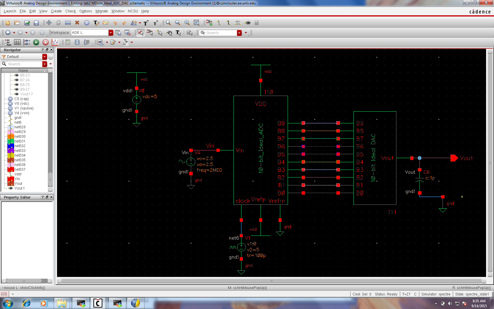
The
following is a description on how to create a symbol view using the
exact same footprint as the Ideal_10-bit_DAC symbol view.
From the Simulation Schematic, the original DAC symbol was modified after copying the directory, then the corresponding cell views were modified.
Refer to images in the 10-Bit DAC Design section.
The following simulations are for validation of a functional design.

As resistive load increases, the output voltage decreases.
As capacitive load increases, the time delay from input to output increases

A combination of both resistive and capacitive load tends to lower the output voltage and create time delays.
If this particular DAC were to drive a 10k Ohms Load, then the output voltage would be reduced to 1/2 the original Vout.
The reson is that 10k Ohms is exactly the R value used in the DAC design, and thus the output resistance as seen from Vout.
By the voltage division principle:
Vout = Vin*(R/(R+R)) = Vin*(1/2)
The following is a brief discuss on switches that do not have a small resistance compared to R.
Assume that the switching resistance of each element is uniform across the ladder network, and non-negligible with respect to R.
The additional switching resistance acts in series with each 2R brach element, and thus contributes to a larger branch resistance.
By the original expression:
Rout = ((((((((..................||2R)+R)||2R)+R)||2R)+R)||2R)+R)||2R
It can be seen that the 2R parallel branches become (2R+Rs), where Rs is the additional switching resistance.
Rout' = ((((((((..................||(2R+Rs))+R)||(2R+Rs))+R)||(2R+Rs))+R)||(2R+Rs))+R)||(2R+Rs)
The effect is to increase the 2R branch resistance and disproportiately modify the voltage drops at each of the nodes.
Hence
the DAC output voltage decreases, time delay increases, and also
distorts the LSB with respect to the other bits because of asymettry in
the ladder network.
Schematic Images taken from CMOS third Edition.
Lab 2 served as the Design of a 10-bit digital-to-analog converter (DAC) and its theory of operation.