Lab description
Final Project consists of the following:
- Design of an 8-bit resettable (input "clear") up/down counter.
- A 31-stage ring oscillator with a buffer for driving a 20 pF off-chip load.
- NAND and NOR gates using 6/0.6 NMOSs and PMOSs.
- An inverter made with a 6/0.6 NMOS and a 12/0.6 PMOS.
- Transistors, both PMOS and NMOS, measuring 6u/0.6u where all 4 terminals of each device are connected to bond pads (7 pads + common gnd pad).
- A 25k resistor implemented using the n-well.
- Voltage divider between the 25k resistor and a 10k resistor.
Lab Report
Up/Down Counter with clear and load
- Before starting the deisgn of the counter I modified some components I had previously created.
- All of the gates used were modified to add a vdd that is local to the circuit.
- I also modified the MUX I had previously created to only use one select pin by adding an inverter inside my design.
- This changes can be seen below along with the new symbol for this MUX.


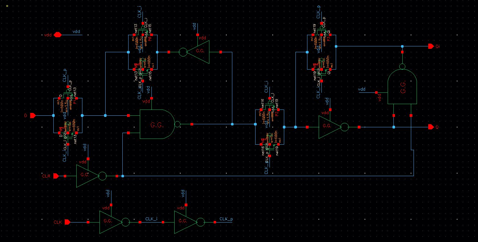
- Then I created a D flip flop to be used in the up/down counter.
- The D flip flop works by maintaining its current value using a loop of inverters, or in this case an inverted and a NAND gate.
- This is then made synchronous by adding transmission gates that are activated by the clock.
- A NAND gates is used in this case to be able to reset the value of the gate back to zero.
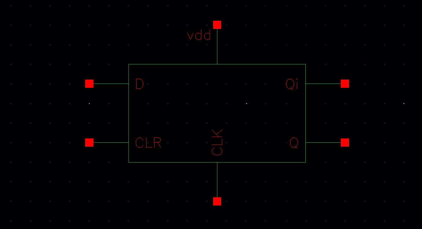
- The full schematic for the D flip floop along with a symbol created for it can be seen below.
- Then I created a schematic to test the operation of the D flip flop created.
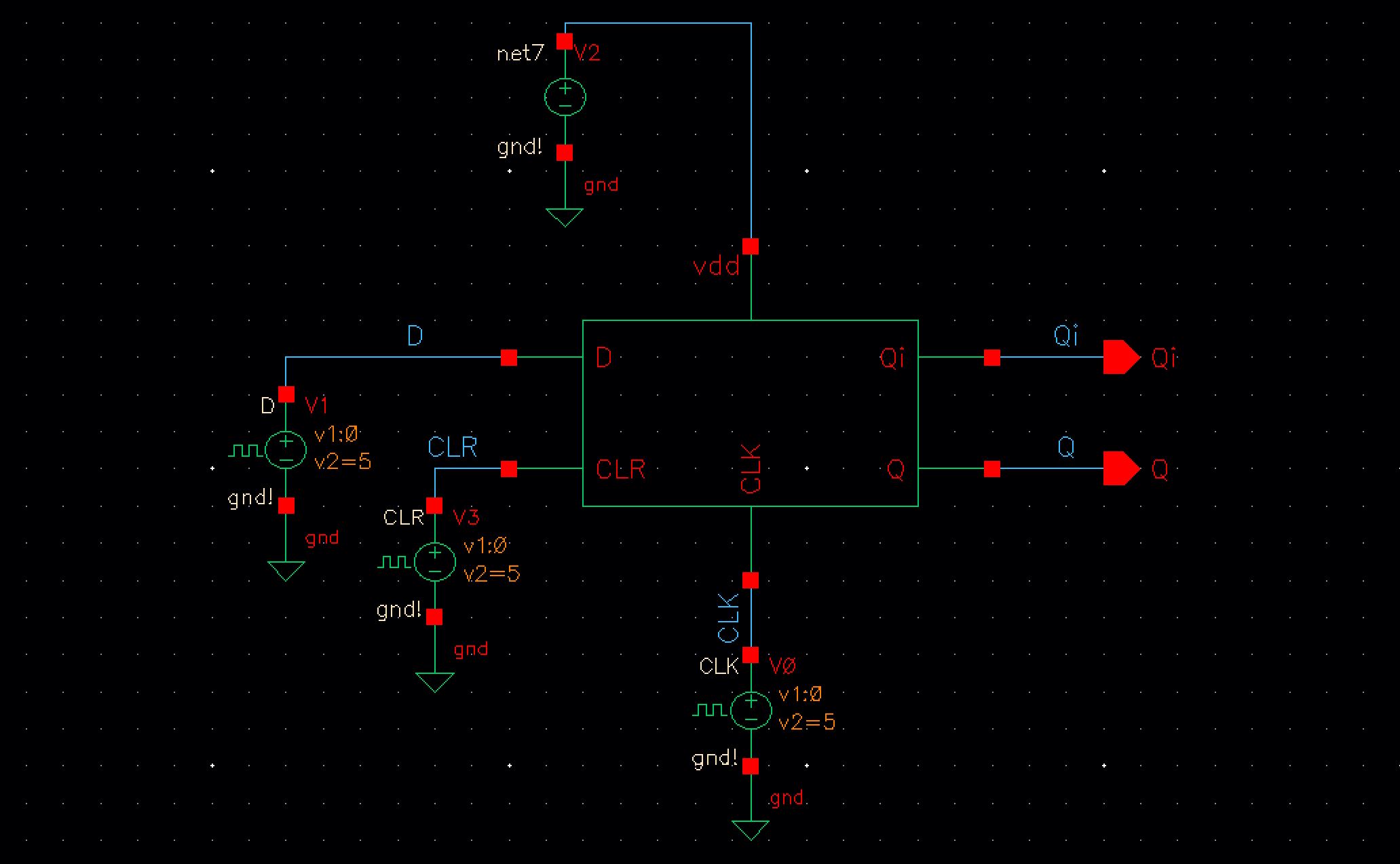
- The results show the correct operation of the D flipp flop.
- The output, Q, becomes what the input, D, is at the rising edge of the clock, and Qi is the inverse of Q.
- When the CLR signal goes high the value of Q resets to zero immediately, and stays there as long as CLR is high.

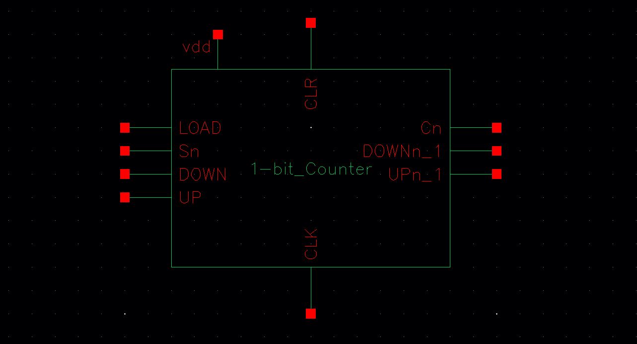
- Then the schematic for one bit of the couter was created.
- The D flip flop created previously was used in conjunction with an XOR gate to create the equivalent of a T flip flop, the output of the D flip flop is fed to the XOR gate and the second input of the XOR gate is the logic that determines when the value on the flip flop will be toggled, when this second input goes high the velue on the flip flop is toggled.
- A MUX was also used to select between the value currently on the flip flop or a new value to be loaded into the flip flop.
- Then a couple of AND gates were used to create the logic that will determine the toggling of the flip flop on the next bit of the counter.
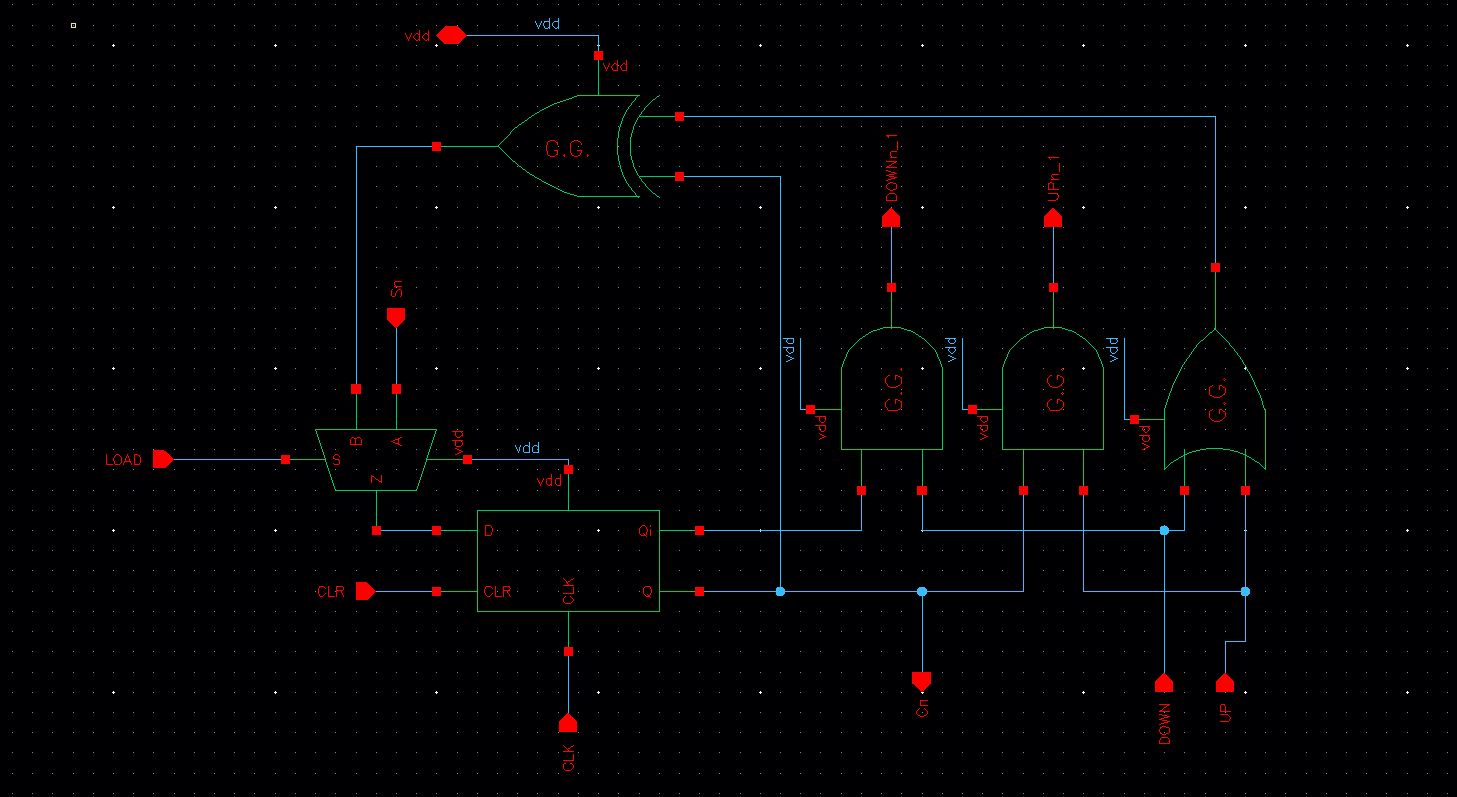
- A symbol was then created for this one bit of the counter to be used to create the 8-bit counter.
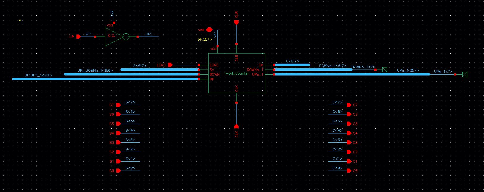
- The 8-bit counter was created using 8 of the 1-bit counters created previously and connecting them together, buses were used for the connections to make the schematic cleaner and easier to read.
- An inverter was used inside this design so that only one UP signal would be needed instead of an UP and a DOWN.
- The full schematic can be seen below.
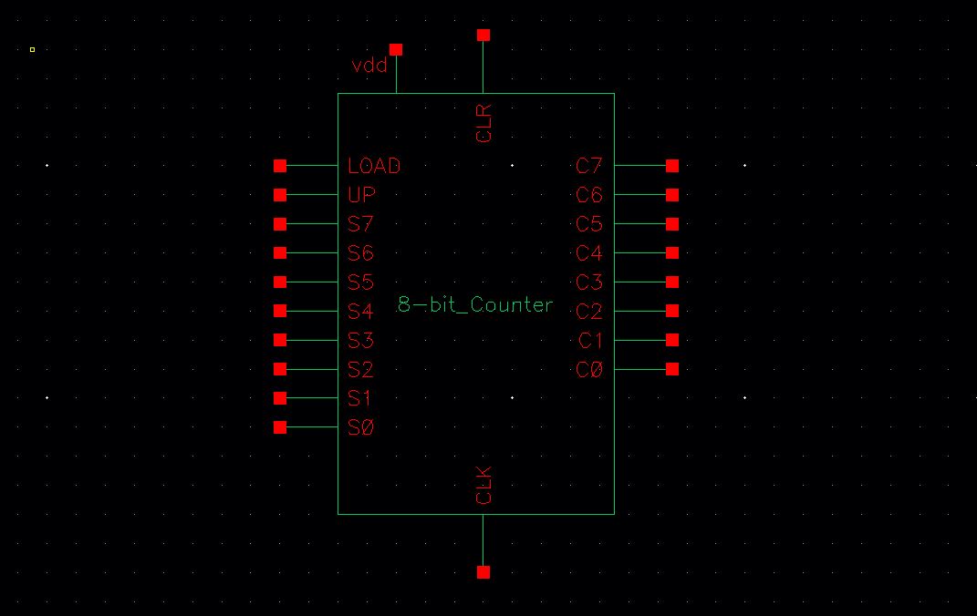
- A symbol was then created for the 8-bit counter.
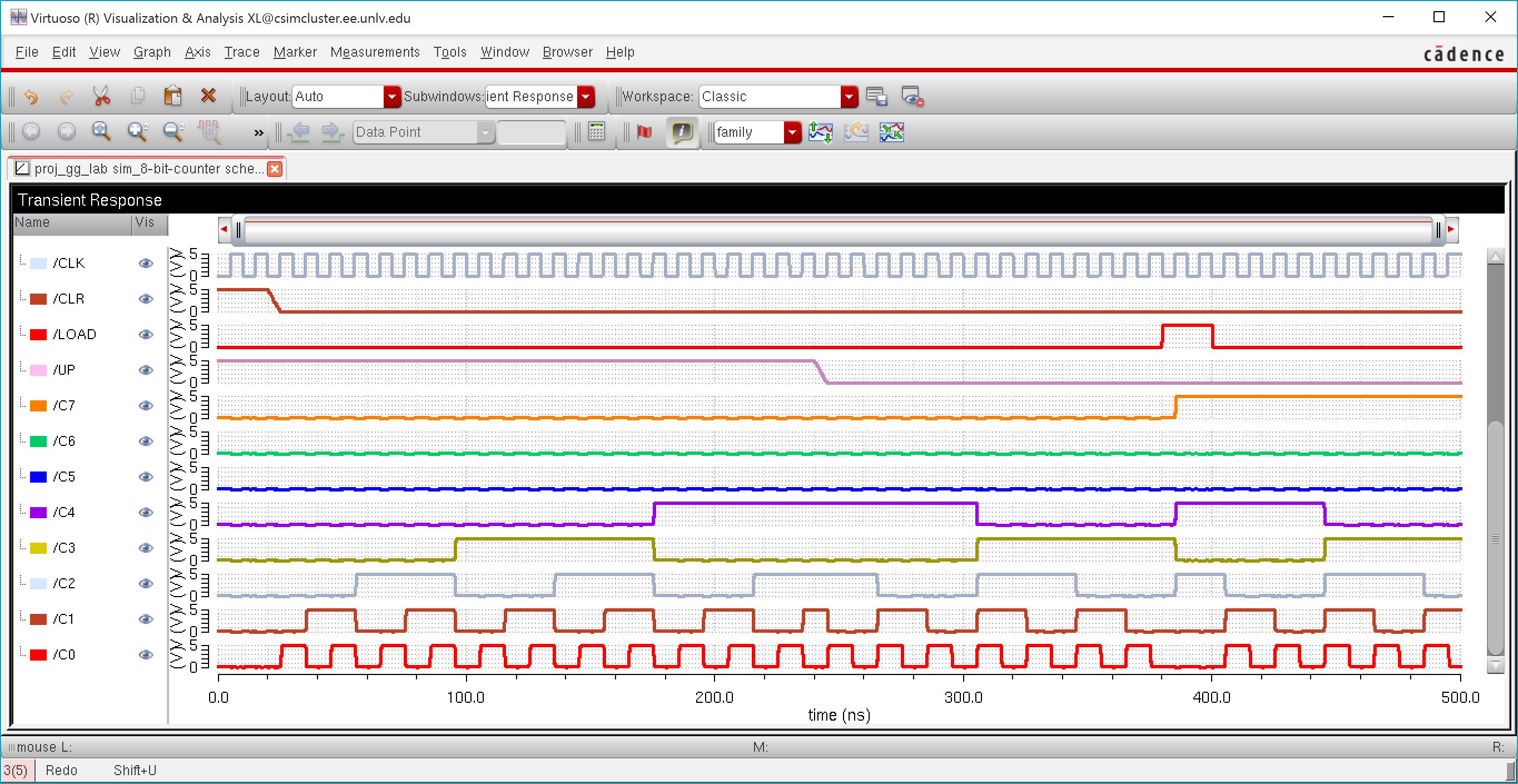
- A schematic was then created to test the operation of the counter.
- The simulation tests all operations of the counter including: counting up, counting down, clearing and laoing a new value.

- The value that will be loaded on this simulation can be seen below, the value is 10010100.

- The operation of the counter can be seen below.
- When the value of the CLR signal is high the counter doesn't change and stays at zero.
- When the value of the UP signal is high the counter counts up on every rising edge of the clock.
- When the value of the UP signal goes low the counter starts to count down from the value that was there before the signal went low.
- When the load signal goes high the value that is on the S pins of the counter is loaded in, this doesn't happen until the rising edge of the clock.
- When the load signal goes low the counter resumes counting up or down, from the value loaded, depending on the status of the UP signal.
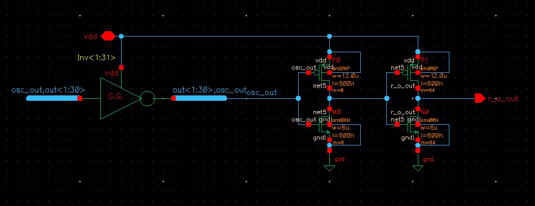
31-stage ring oscillator with buffer
- The schematic for the ring oscillator can be seen below.
- The ring oscillator was made with buses.
- The bufffer was sized with a multiplier of 8 and 64.
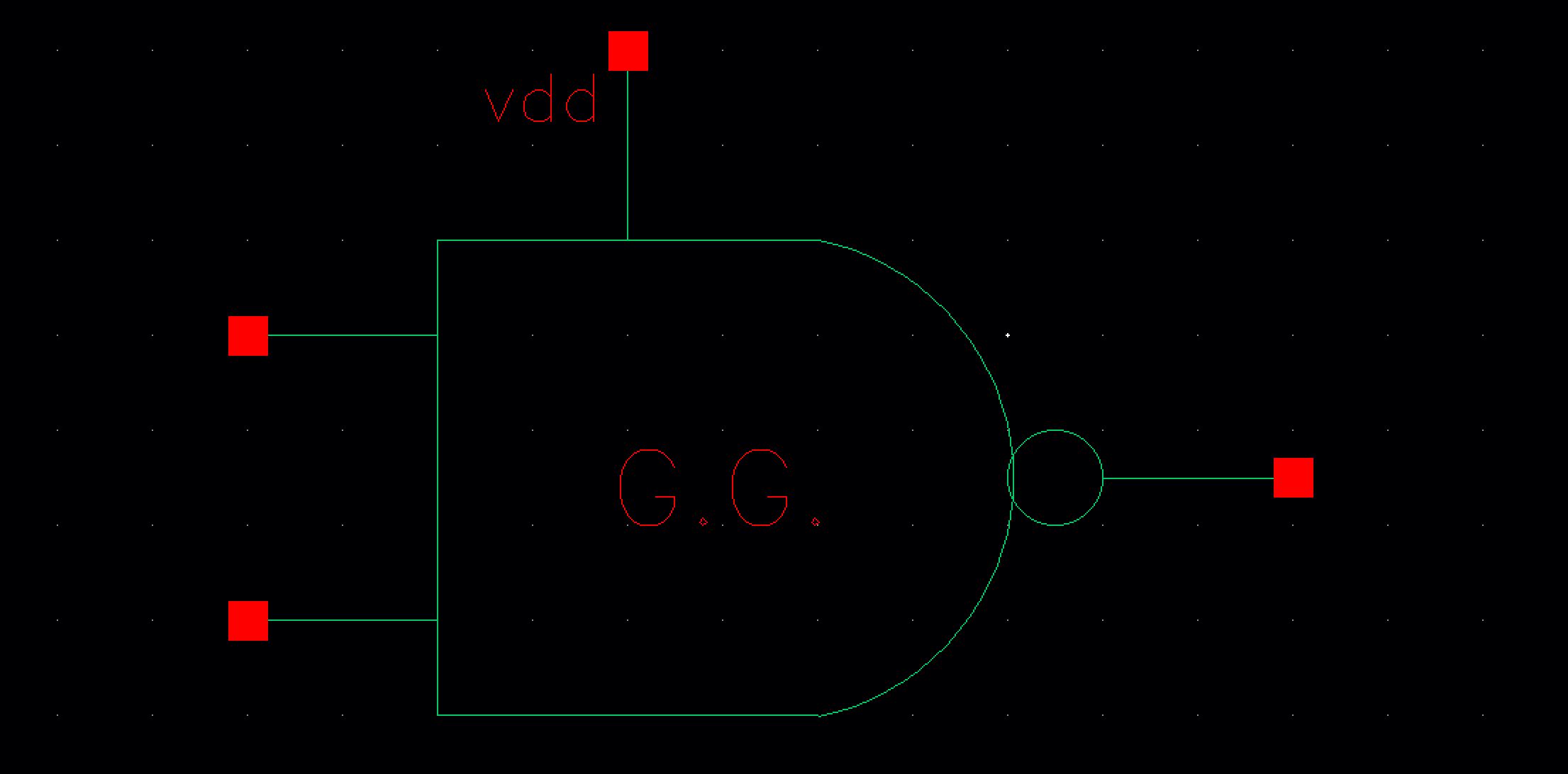
- A symbol was also created from this schematic.

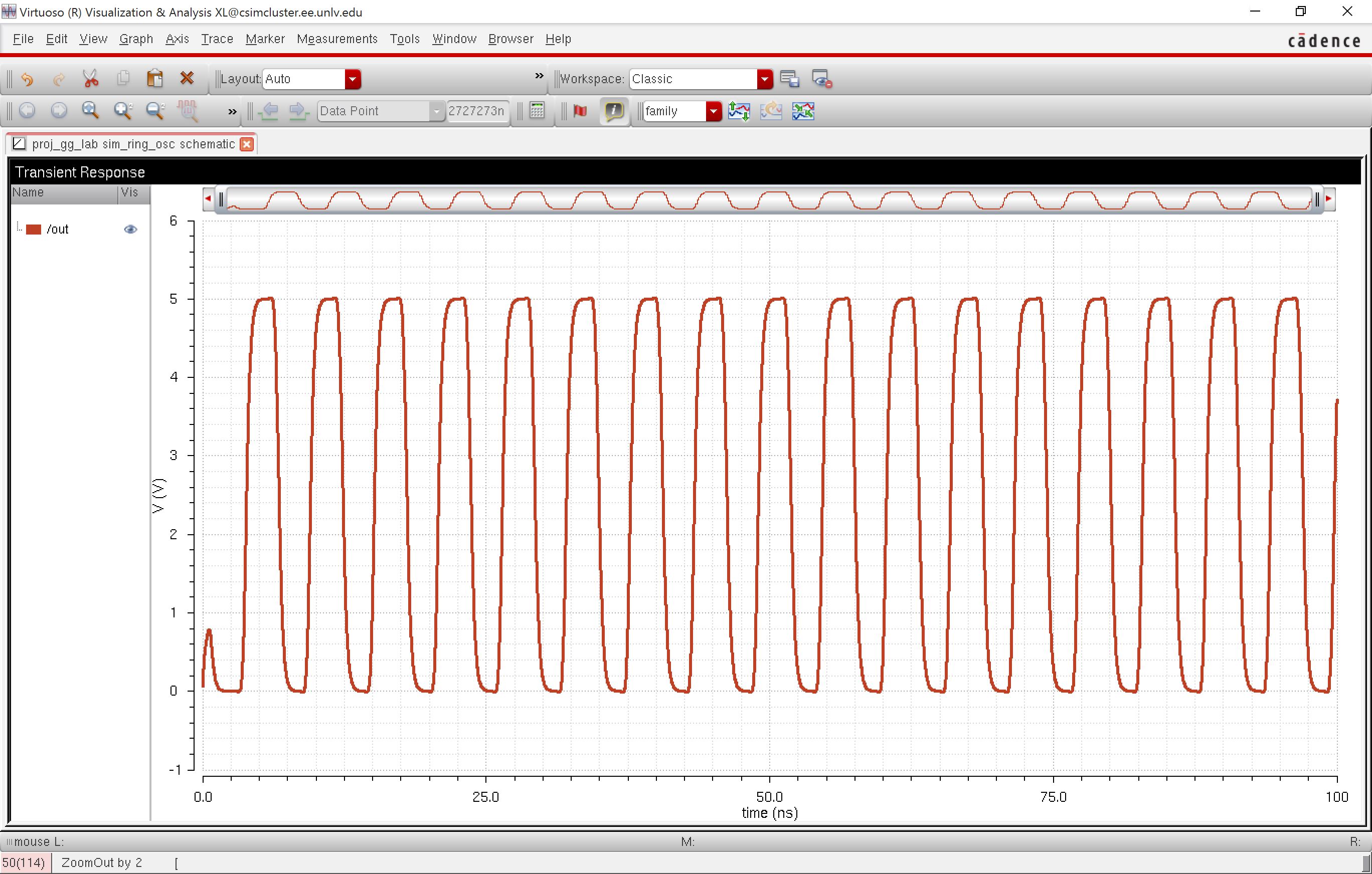
- A schematic was then made to simulate the operation of the ring oscillator.
- The 20pF off-chip load was added here.
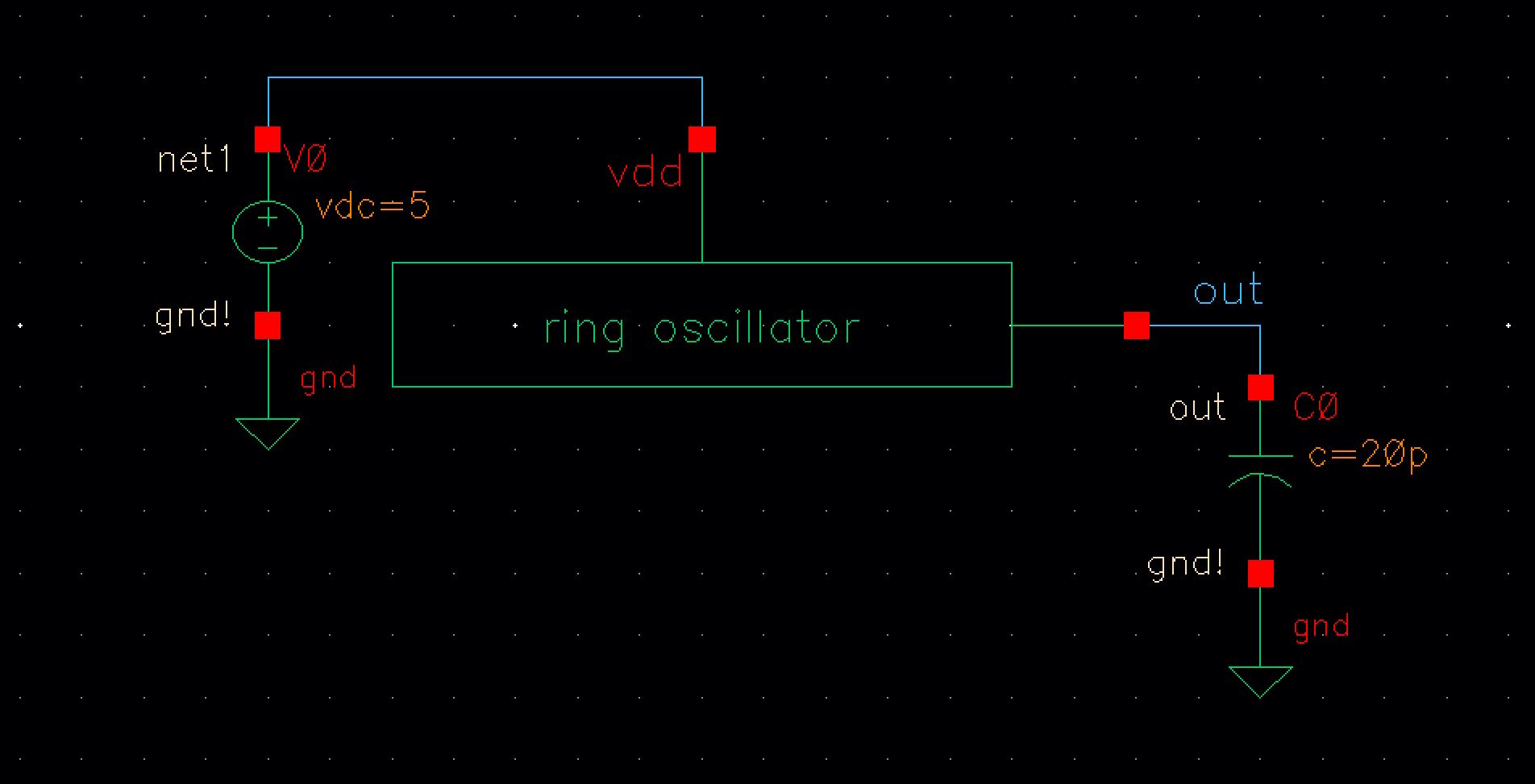
- The results of the simulation can be seen below.
- The buffer we added is enough to drive the load all the way to vdd and ground.

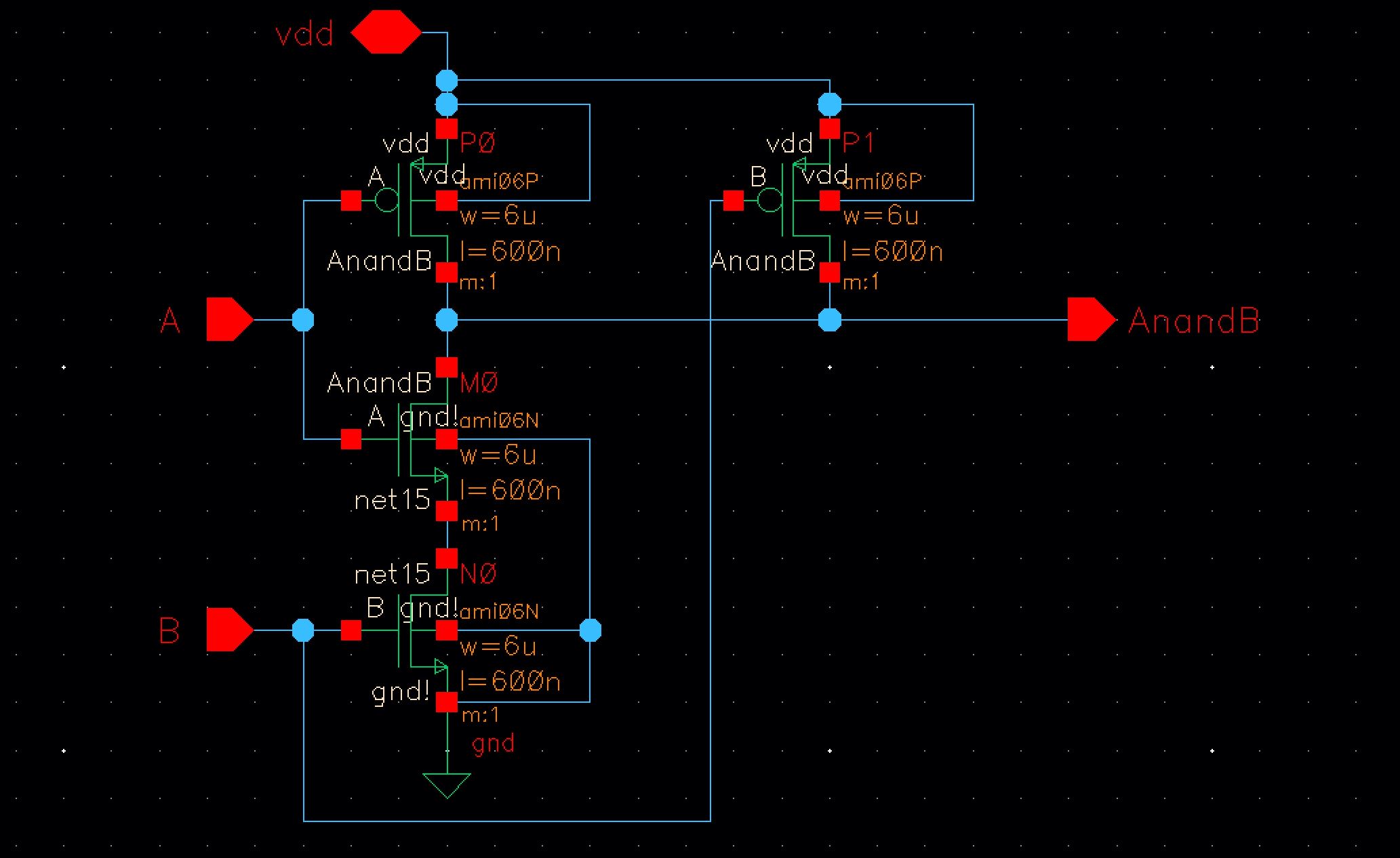
NAND and NOR gates
- The schematic for the NAND gate was created using 6u/0.6u PMOS and NMOS.
- A symbol was also created from the schematic.
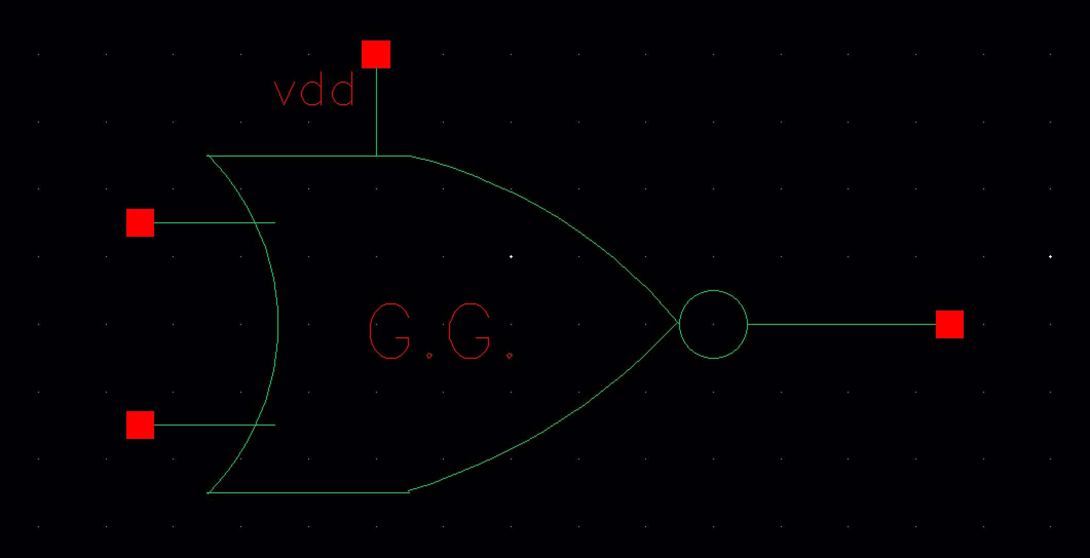
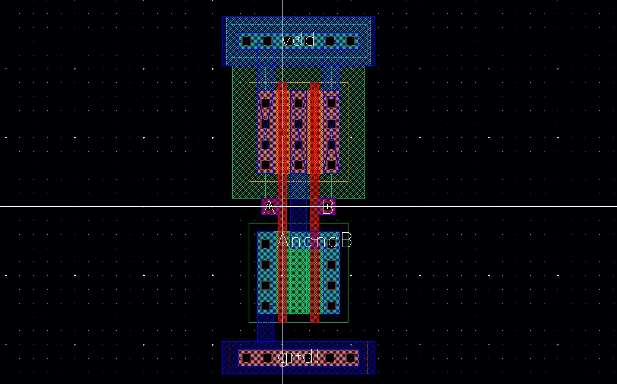
- The schematic for the NOR gate was created using 6u/0.6u PMOS and NMOS.
- A symbol was also created from the schematic.

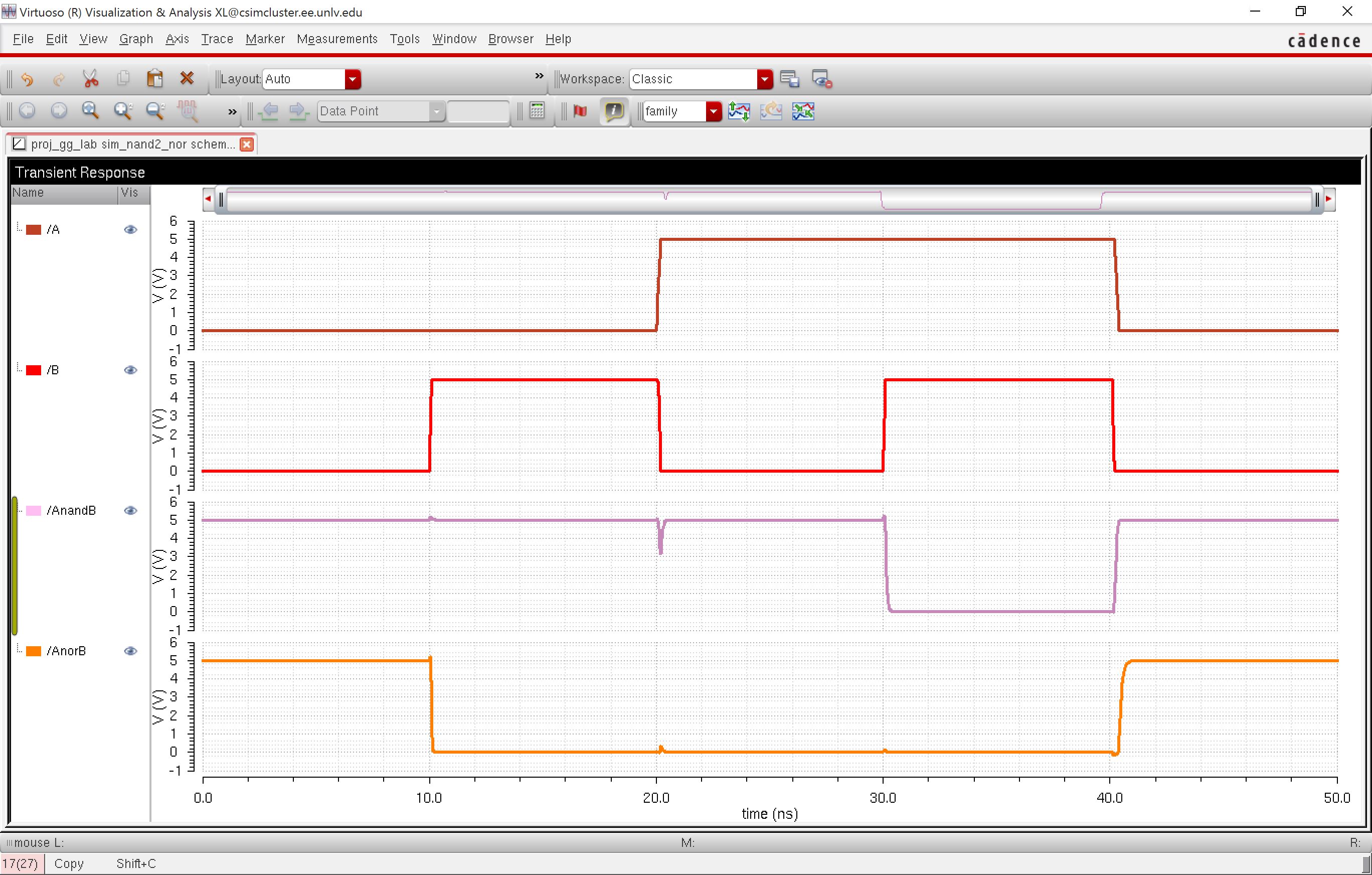
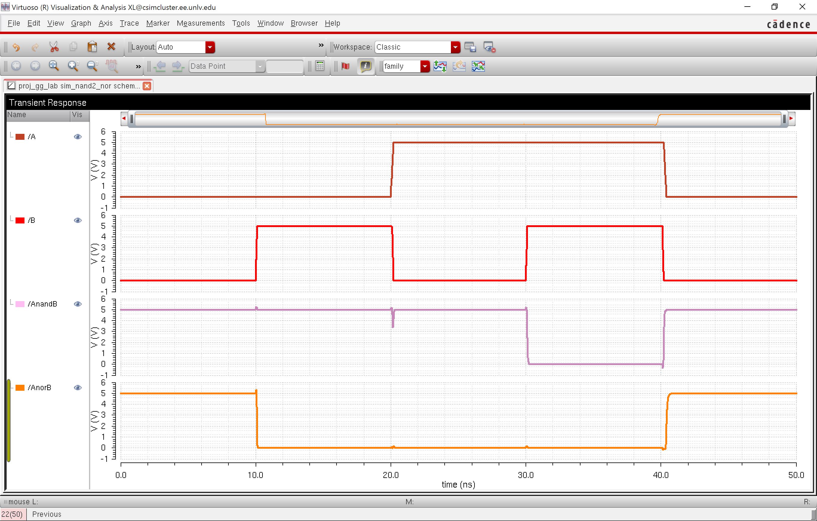
- A schematic was then created to test the operation of the two gates.
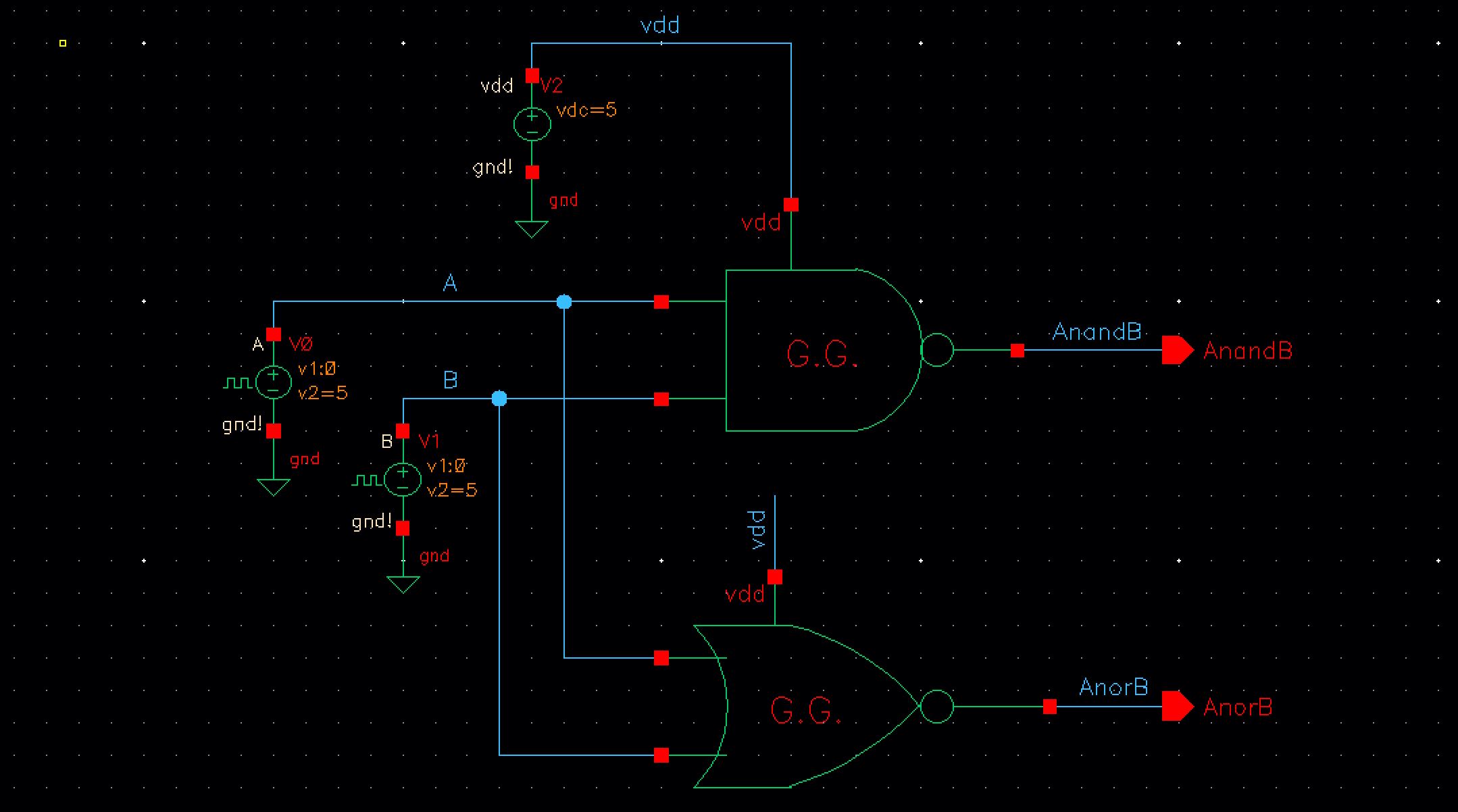
- The results obtained were what is expected from these gates.
| A | B | AnandB | AnorB |
| 0 | 0 | 1 | 1 |
| 0 | 1 | 1 | 0 |
| 1 | 0 | 1 | 0 |
| 1 | 1 | 0 | 0 |
Inverter
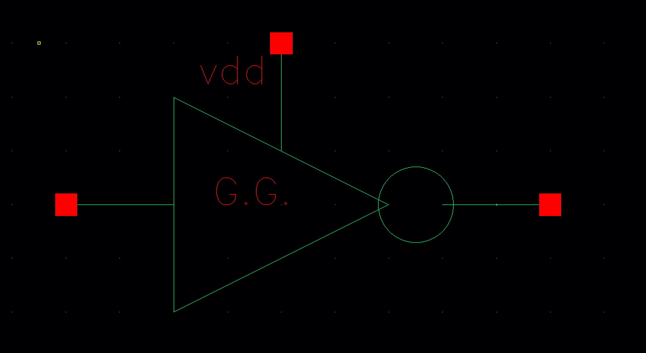
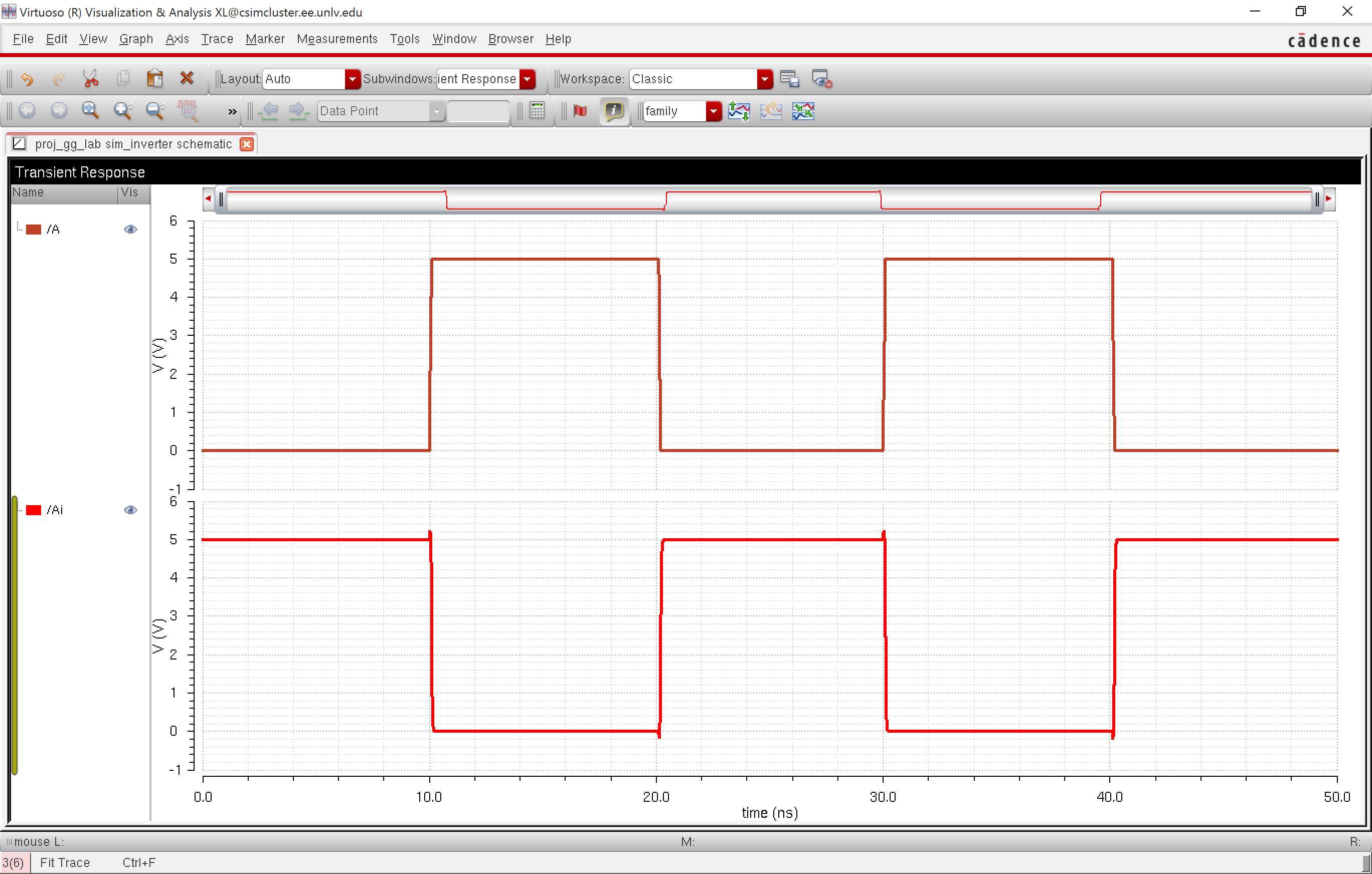
- The schematic for the inverter was created using 12u/0.6u PMOS and 6u/0.6u NMOS.
- A symbol was also created from the schematic.

- A schematic was then created to test the operation of the inverter.

- The results obtained were what is expected, the output is the opposite of the input.
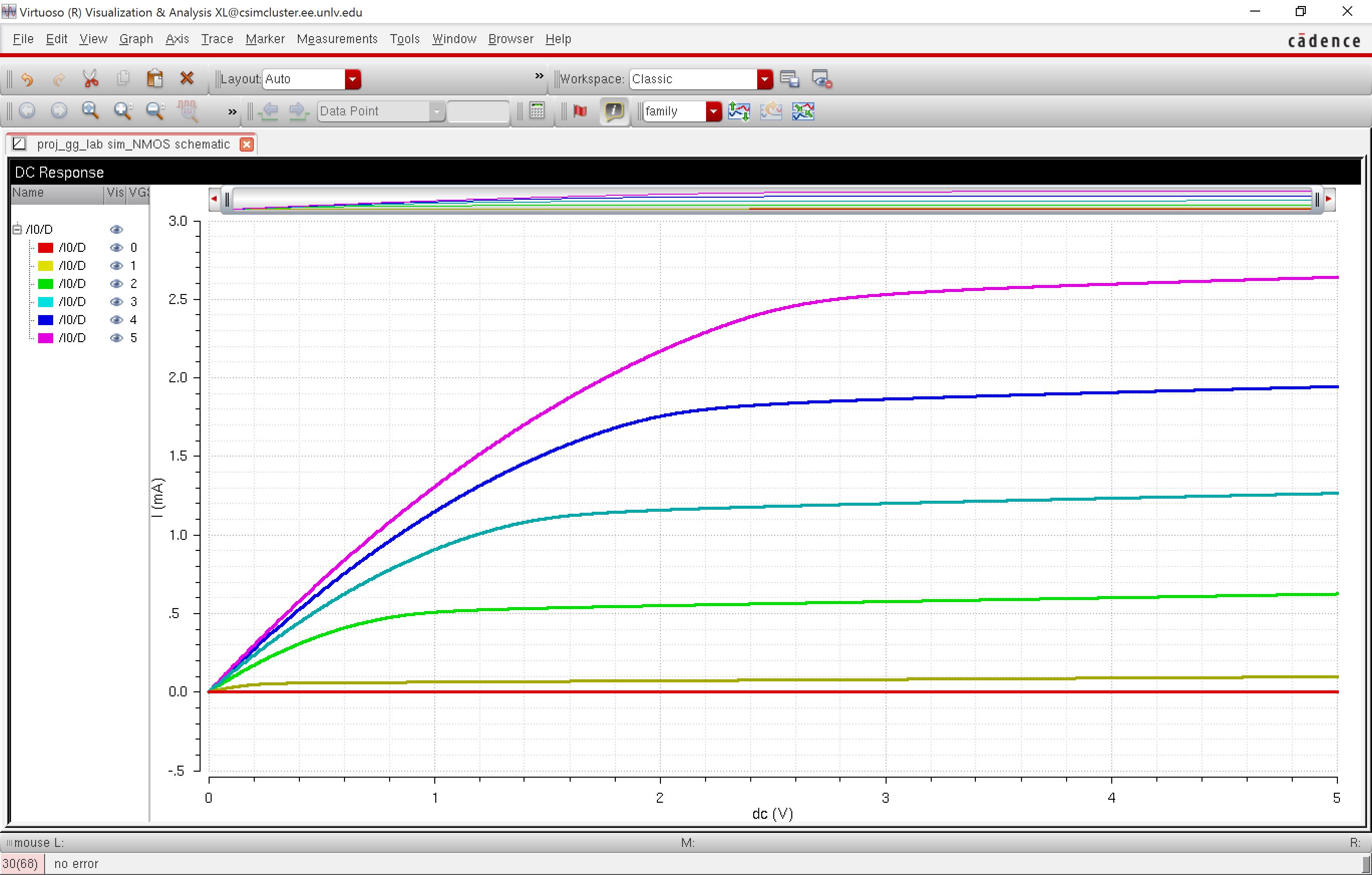
NMOS and PMOS transistors
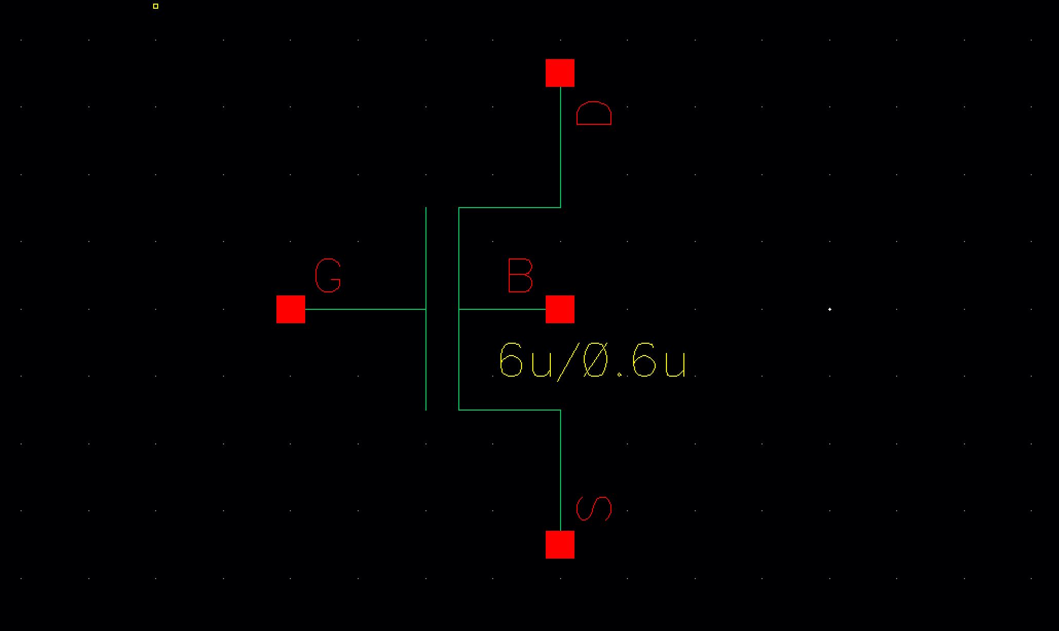
- A schematic was then created for a 6u/0.6u NMOS transistor with connections to all 4 terminals.
- A symbol was also created for this schematic.

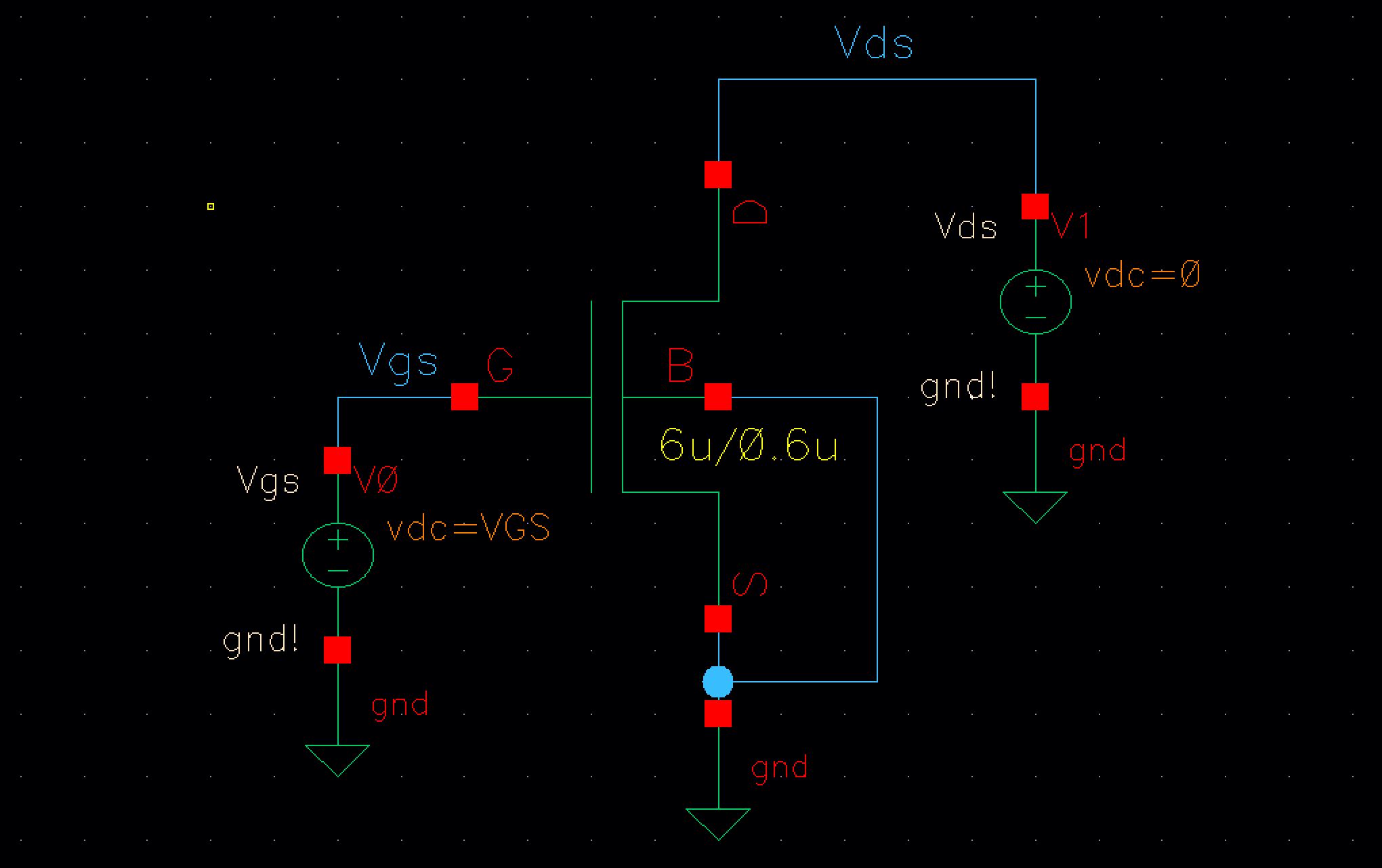
- A schematic was then created to simulate the operation of this transistor.
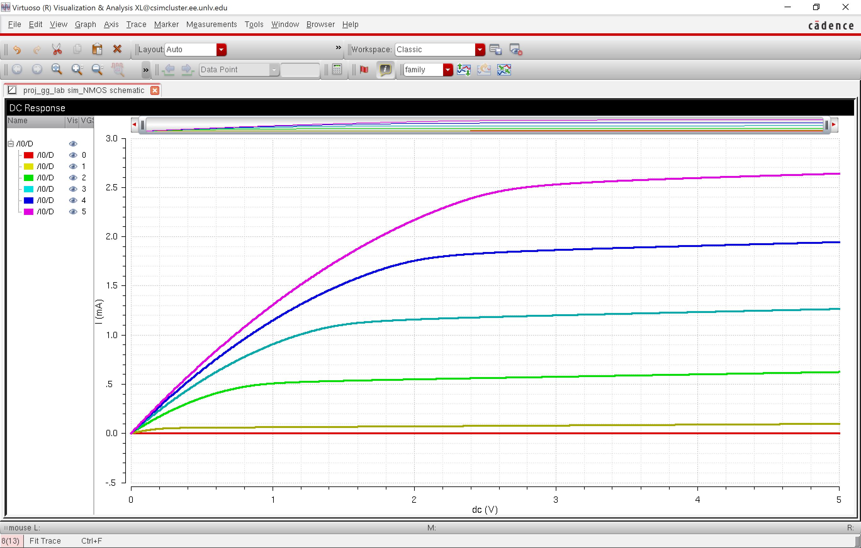
- The resulting transistor curve can be seen below.
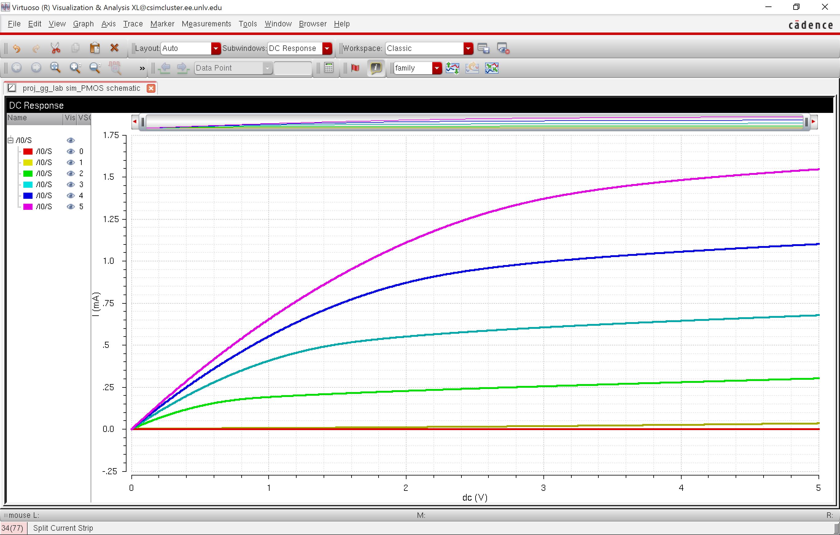
- A schematic was then created for a 6u/0.6u PMOS transistor with connections to all 4 terminals.
- A symbol was also created for this schematic.
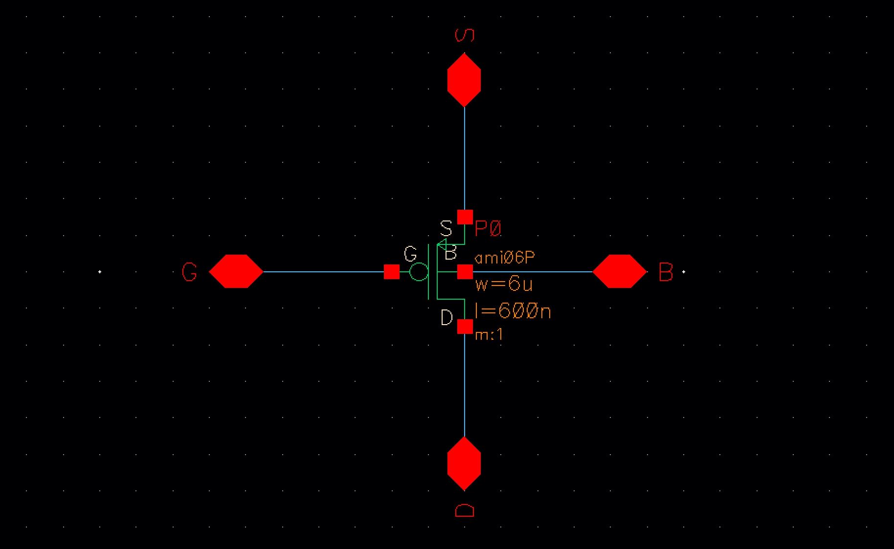

- A schematic was then created to simulate the operation of this transistor.
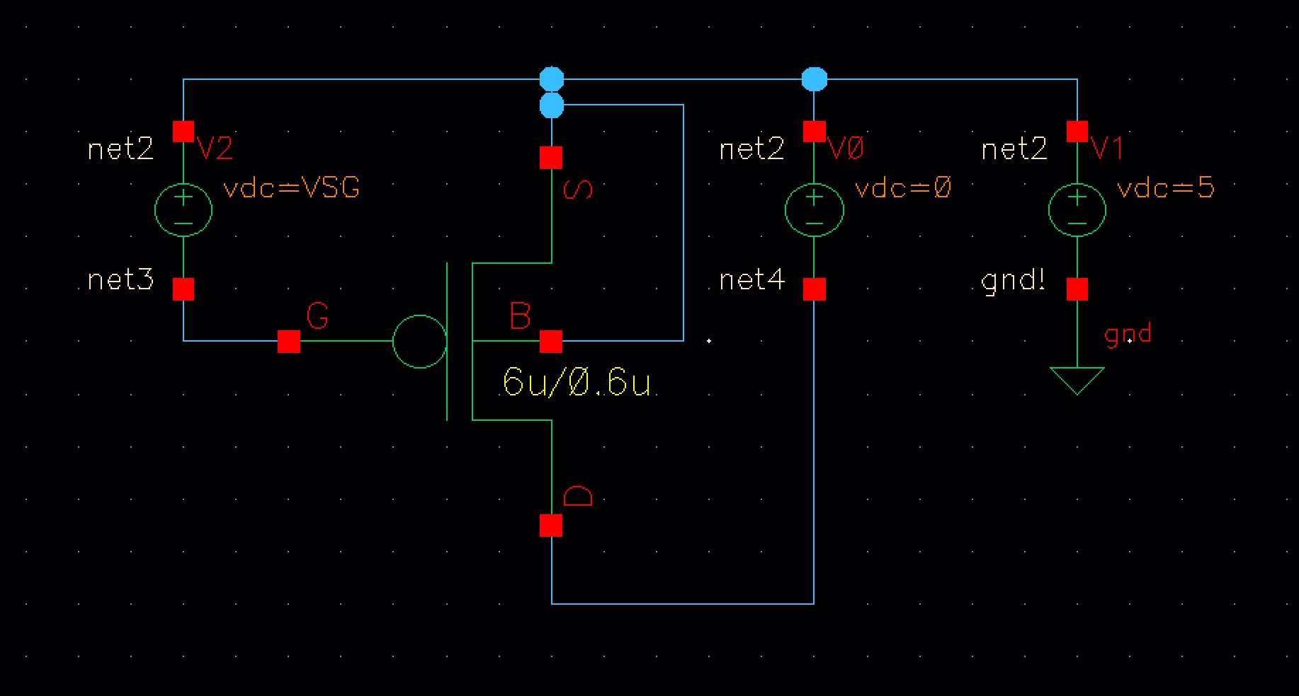
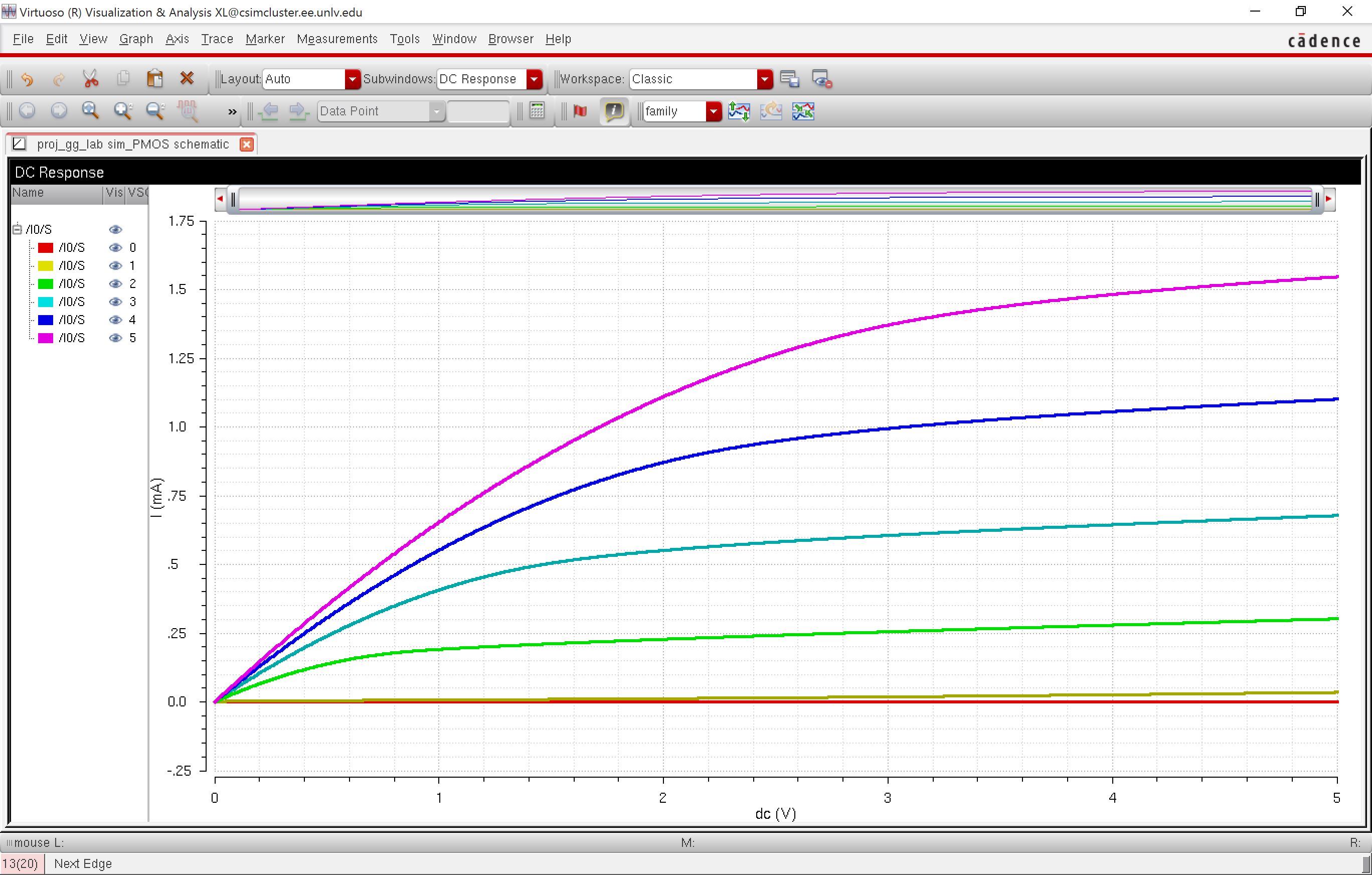
- The resulting transistor curve can be seen below.
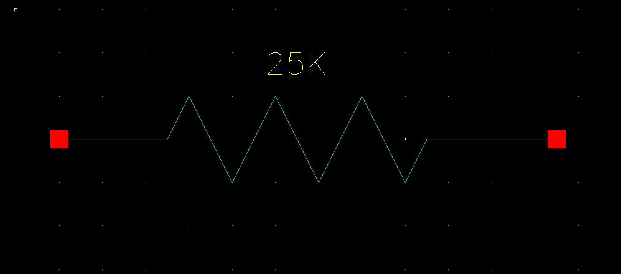
25k resistor
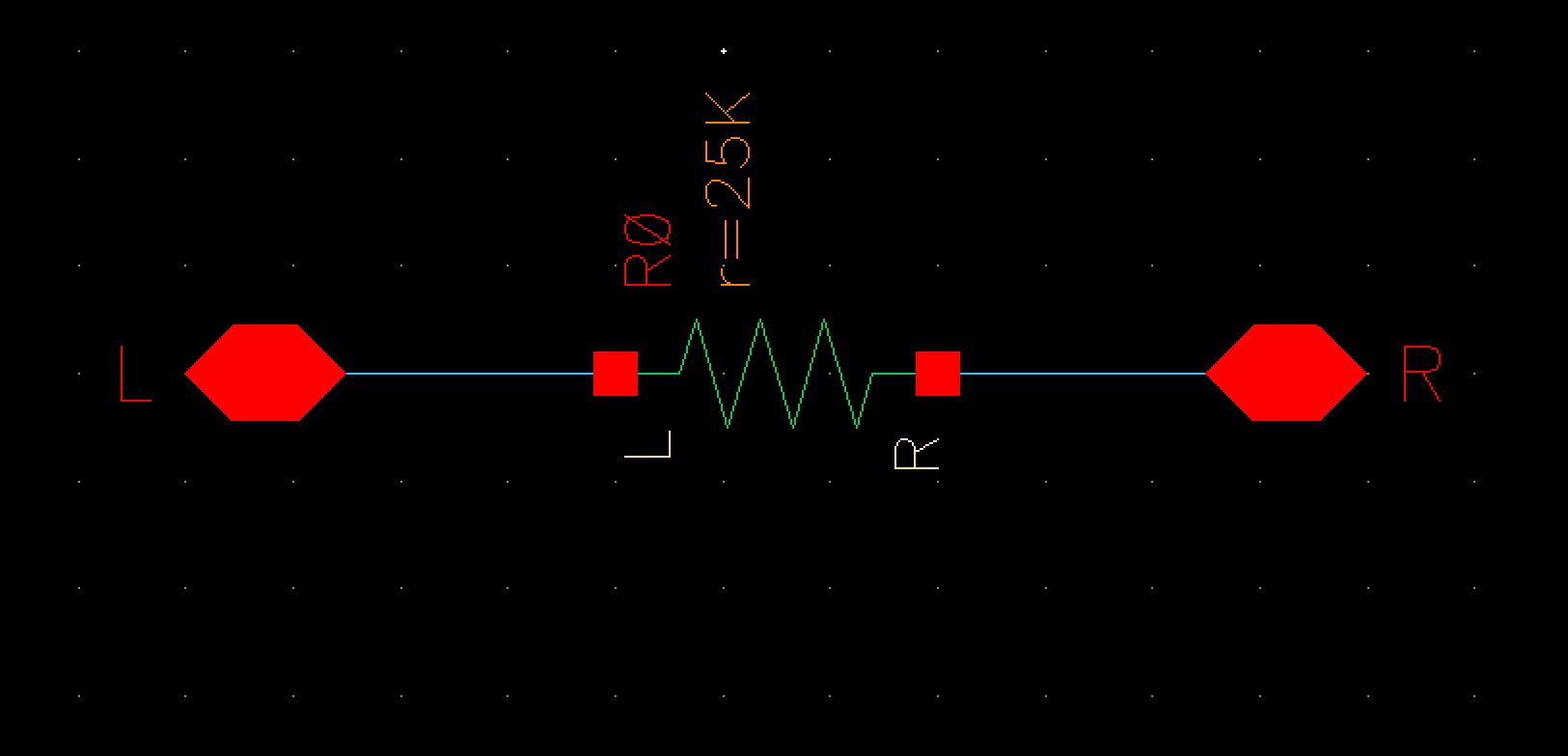
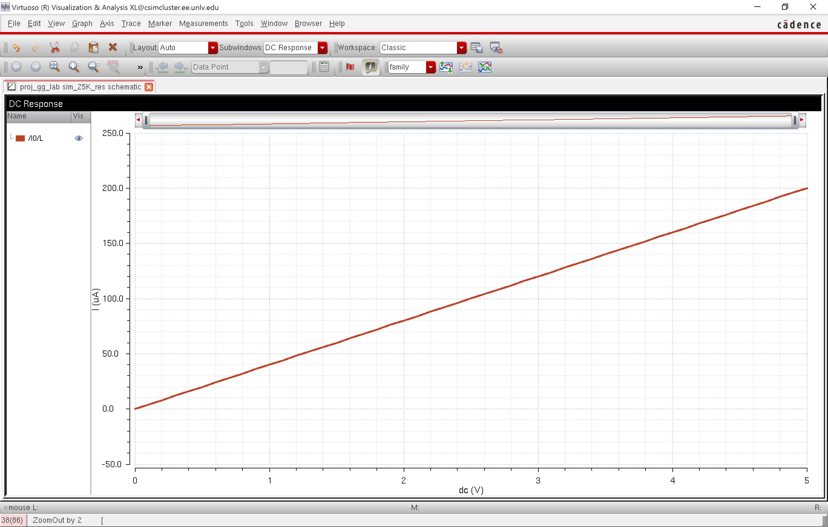
- A schematic for a 25k resistor with connections to both pads was then created.
- A symbol was also created for this schematic.
- A schematic was then created to simulate the operation of the resistor.

- The results are what is expected from thiss resistor.
- The input voltage is varied from 0V to 5V.
- At 0V there is no current flowing through the resistor.
- At 5V there are 200mA flowing through the resistor wich is equal to 5/25K.

Voltage divider
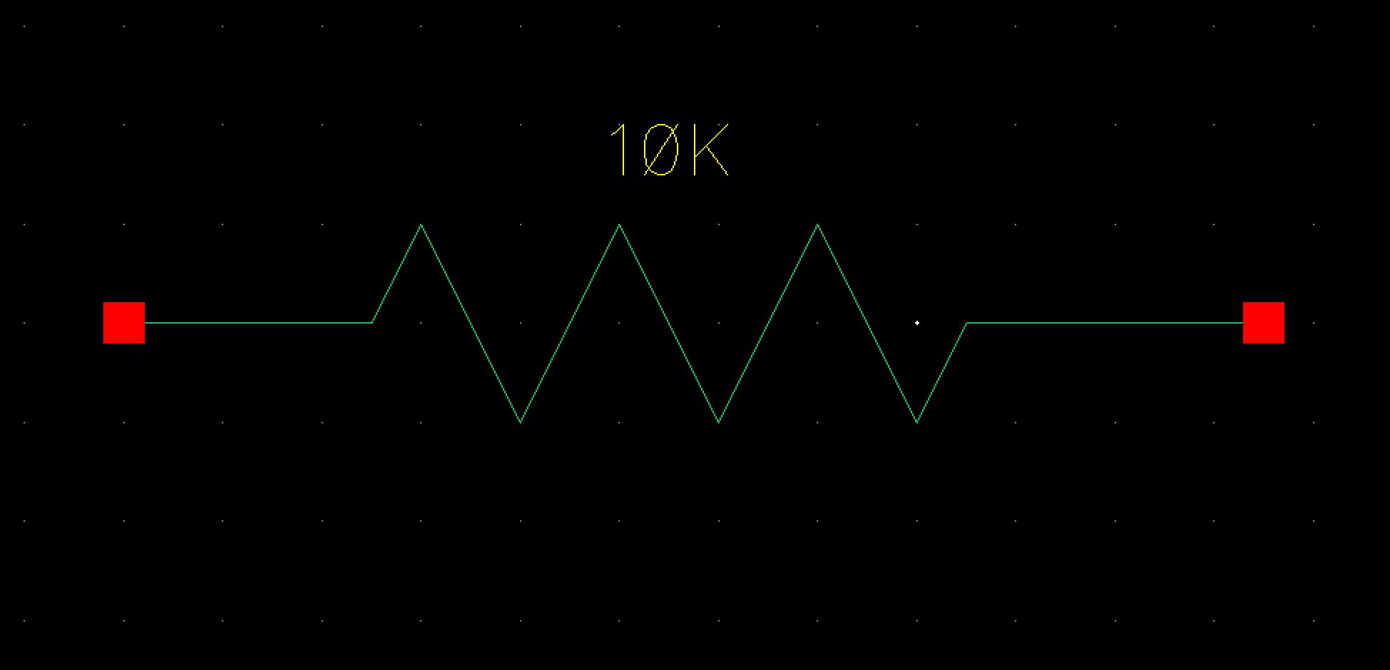
- In order to make the voltage divider first we had to create the schematic and symbol for a 10k resistor.

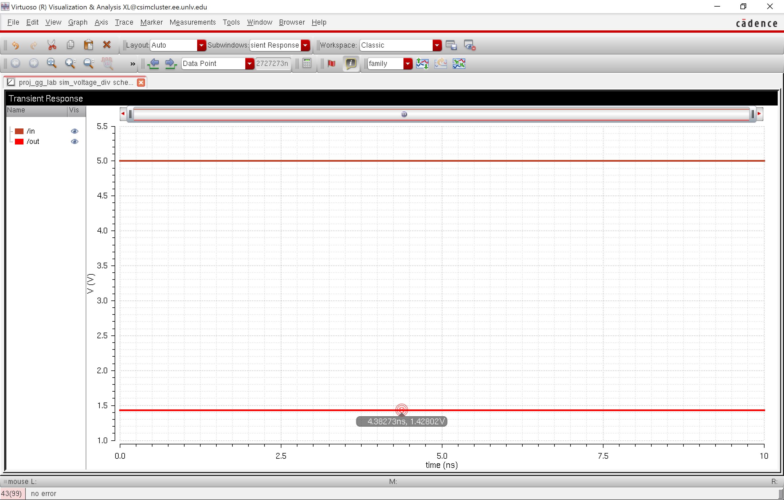
- Then the schematic for the voltage divider was created, using the 25k ressitor previously created and the 10k resistor that was just created.

- The expected result is the following:

- The results obtained from the simulation are the same as our calculations.

Layouts
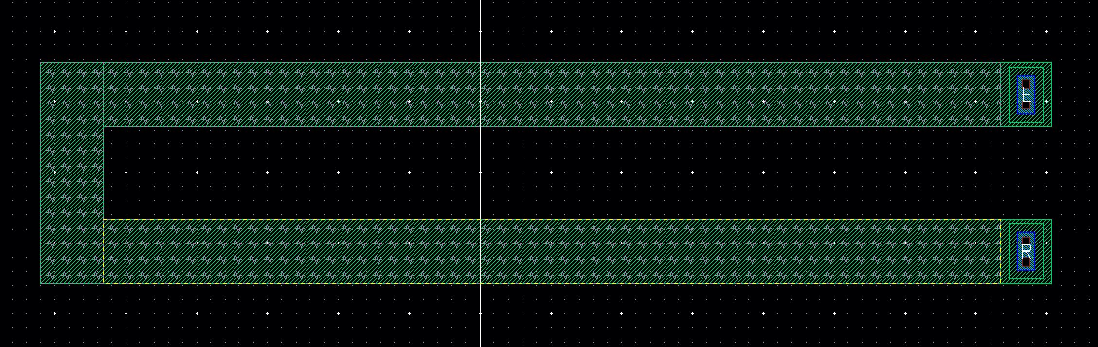
- Once the schematics for our components were working the layouts for them were created.
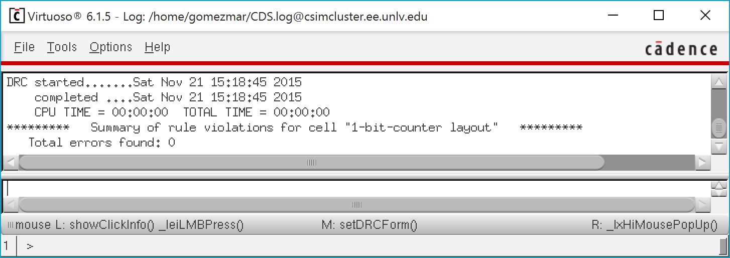
- I started out by creating the layout for the D-Flip Flop to be used on the counter.
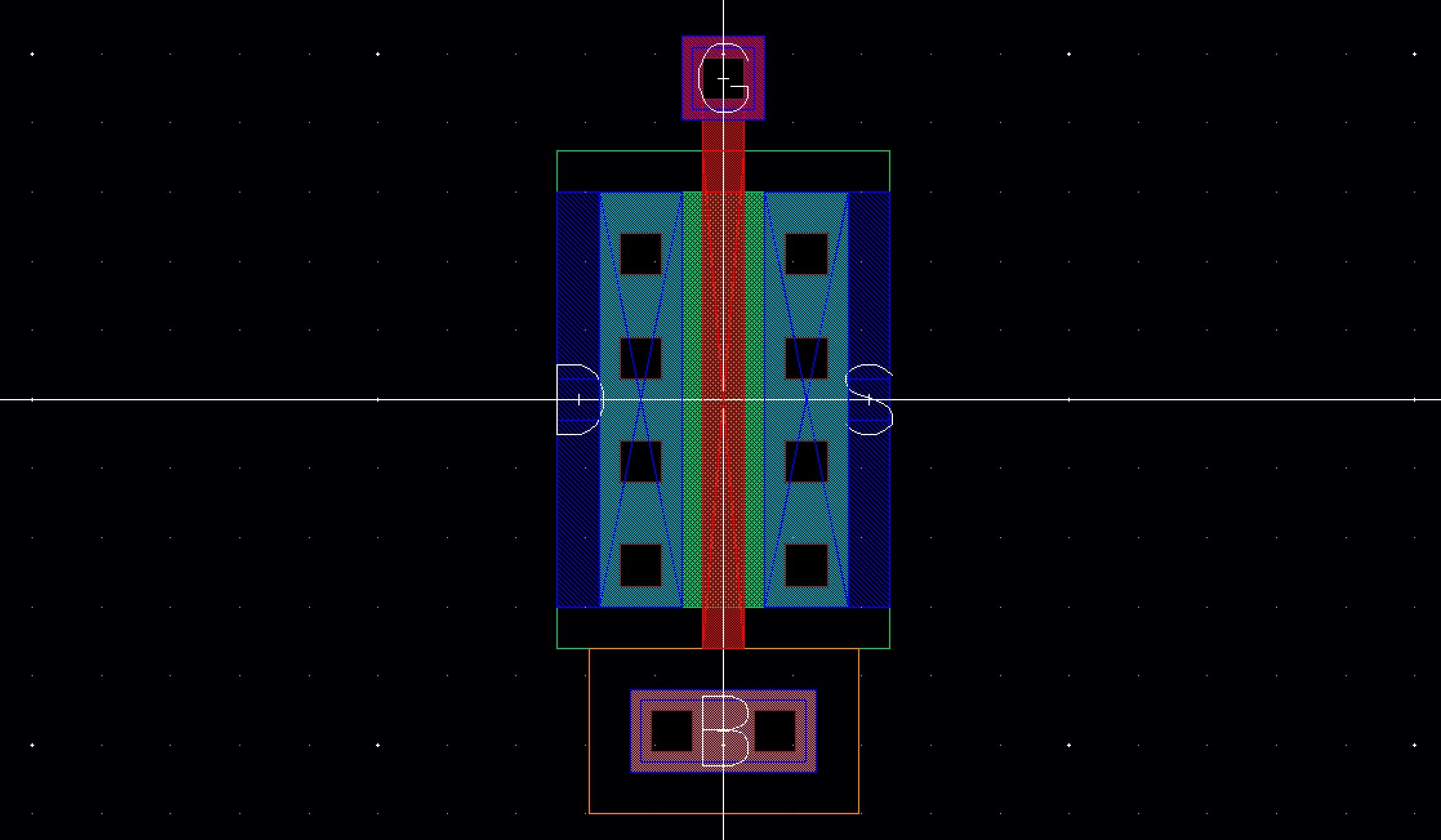
- The layout can be seen below.
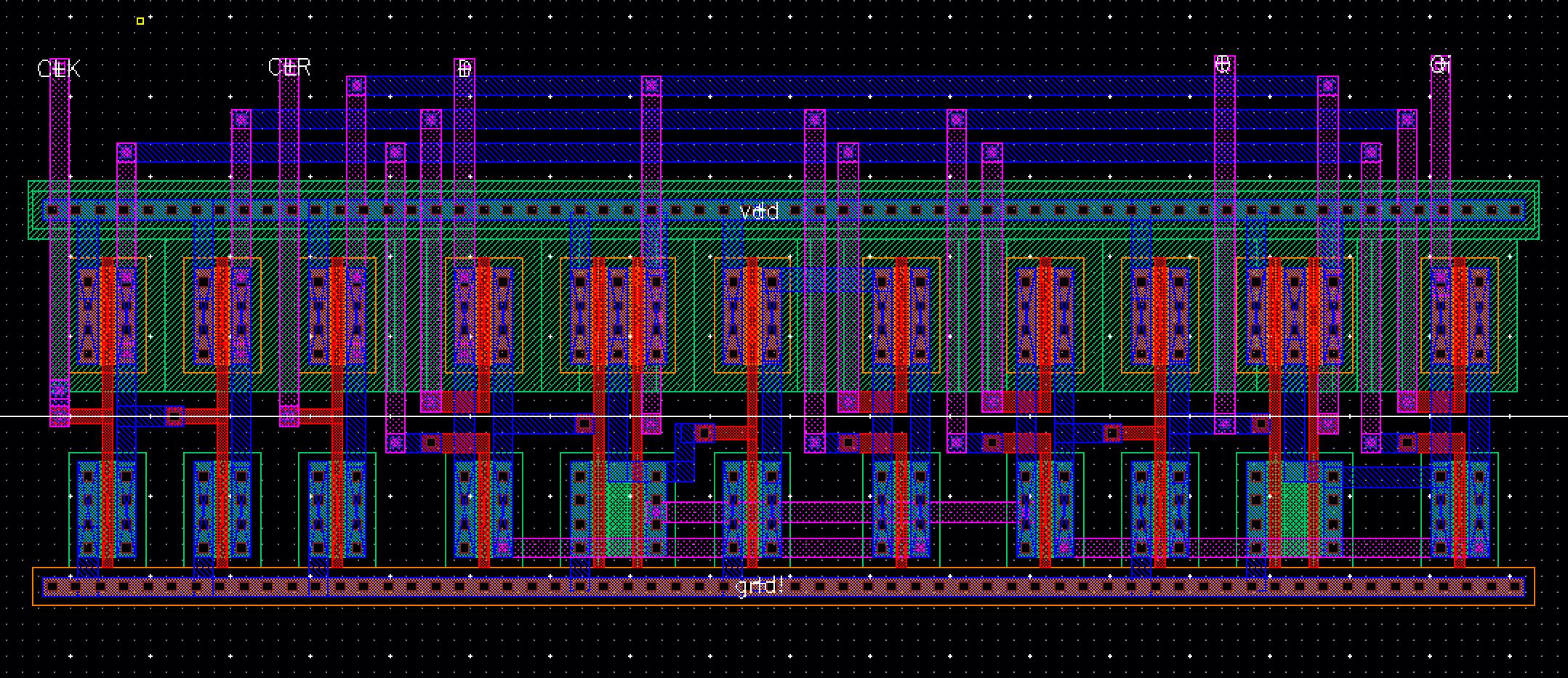
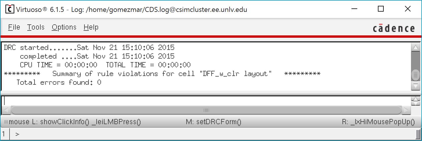
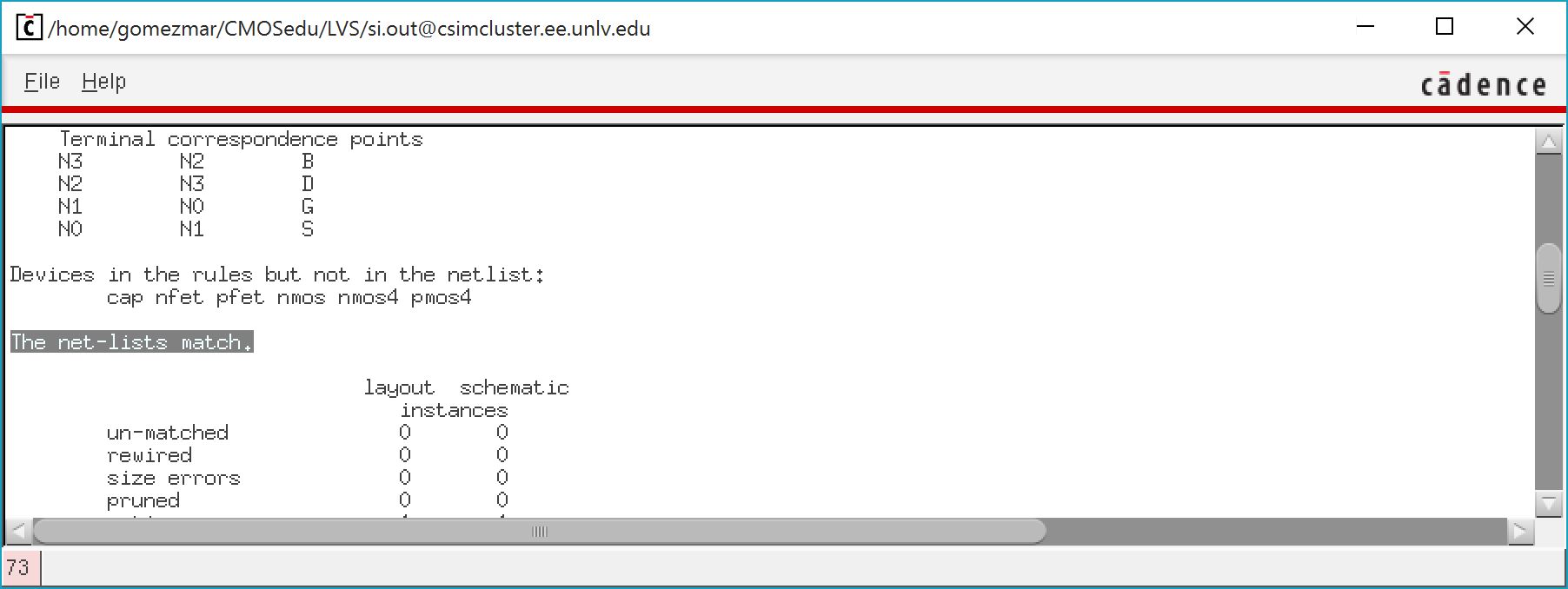
- A DRC check was then performed on the layout to make sure there were no errors.
- An LVS was also performed to ensure the layout matched the schematic.

- Once this was created the layout for 1-bit of our counter was created.
- The D-Flip Flop that was previously created was used here.
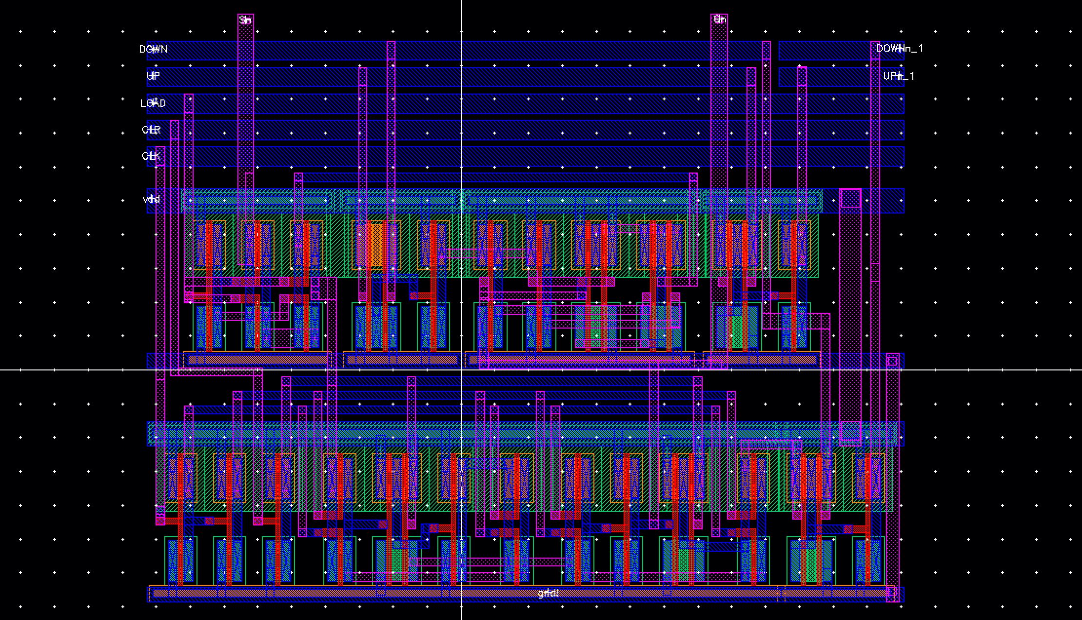
- A DRC check was then performed on the layout to make sure there were no errors.
- An LVS was also performed to ensure the layout matched the schematic.

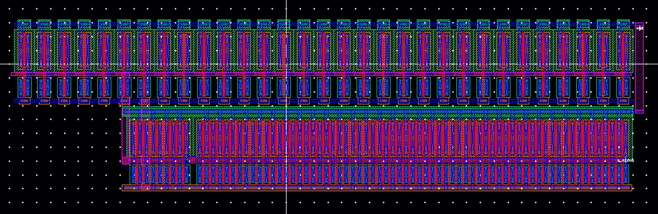
- Then the layout for the complete 8-bit counter was created using 8 of the 1-bit counters previously created.
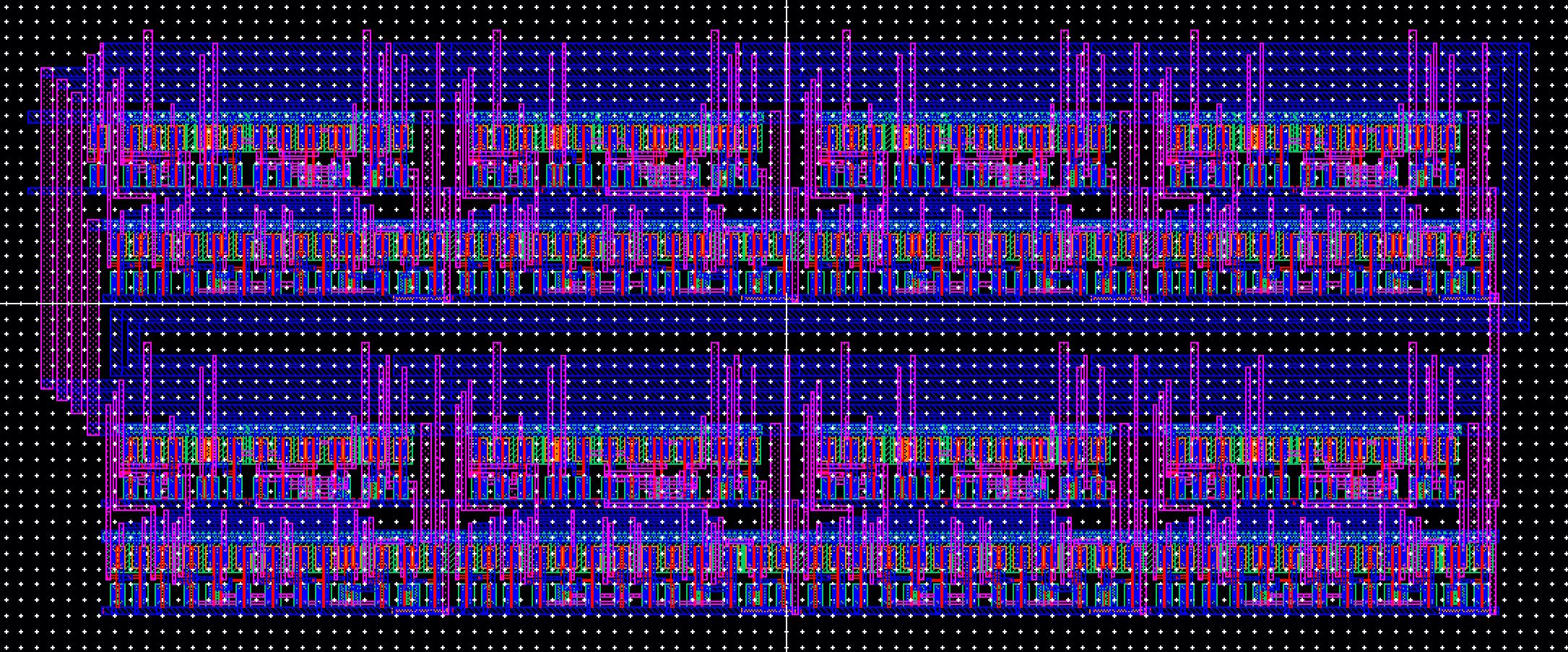

- A DRC check was then performed on the layout to make sure there were no errors.
- An LVS was also performed to ensure the layout matched the schematic.


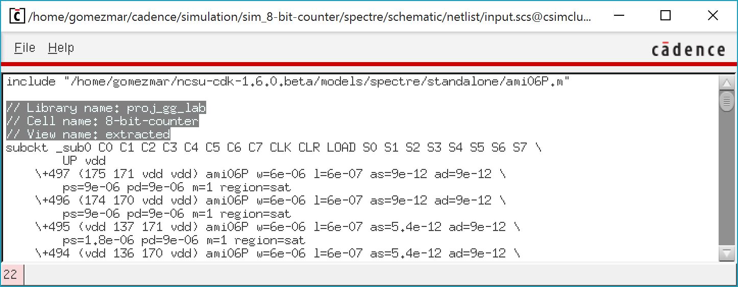
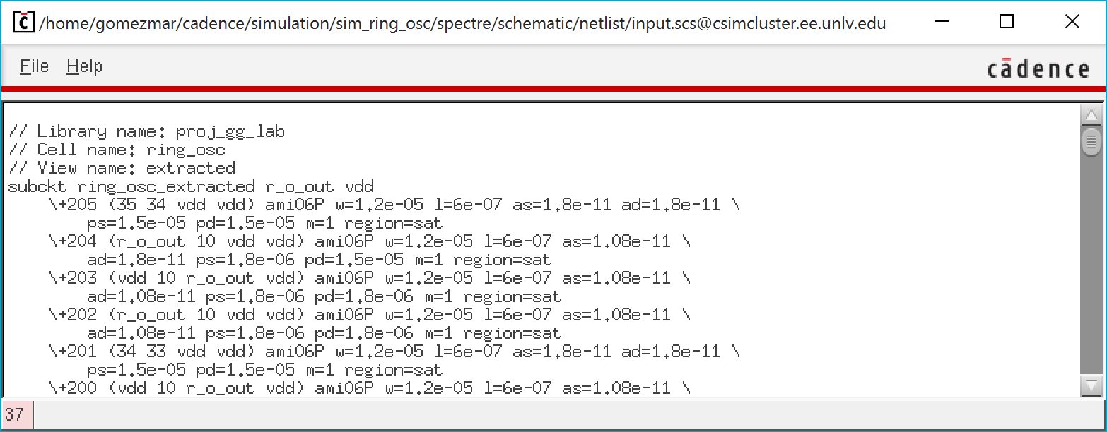
- To ensure there were no problems with the layout a simulation was performed using the extracted view.
- The results obtained were the same as when the simulation was performed using the schematic further proving that the layout is correct.

- Then the layout for the 31-stage ring oscilator with a buffer was created.
- A DRC check was then performed on the layout to make sure there were no errors.
- An LVS was also performed to ensure the layout matched the schematic.


- To ensure there were no problems with the layout a simulation was performed using the extracted view.
- The results obtained were the same as when the simulation was performed using the schematic further proving that the layout is correct.
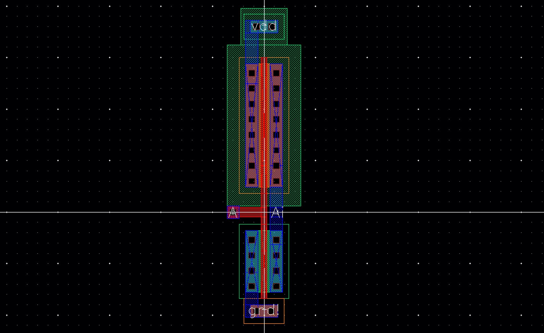
- Then the layout was made for the NAND gate.
- A DRC check was then performed on the layout to make sure there were no errors.
- An LVS was also performed to ensure the layout matched the schematic.

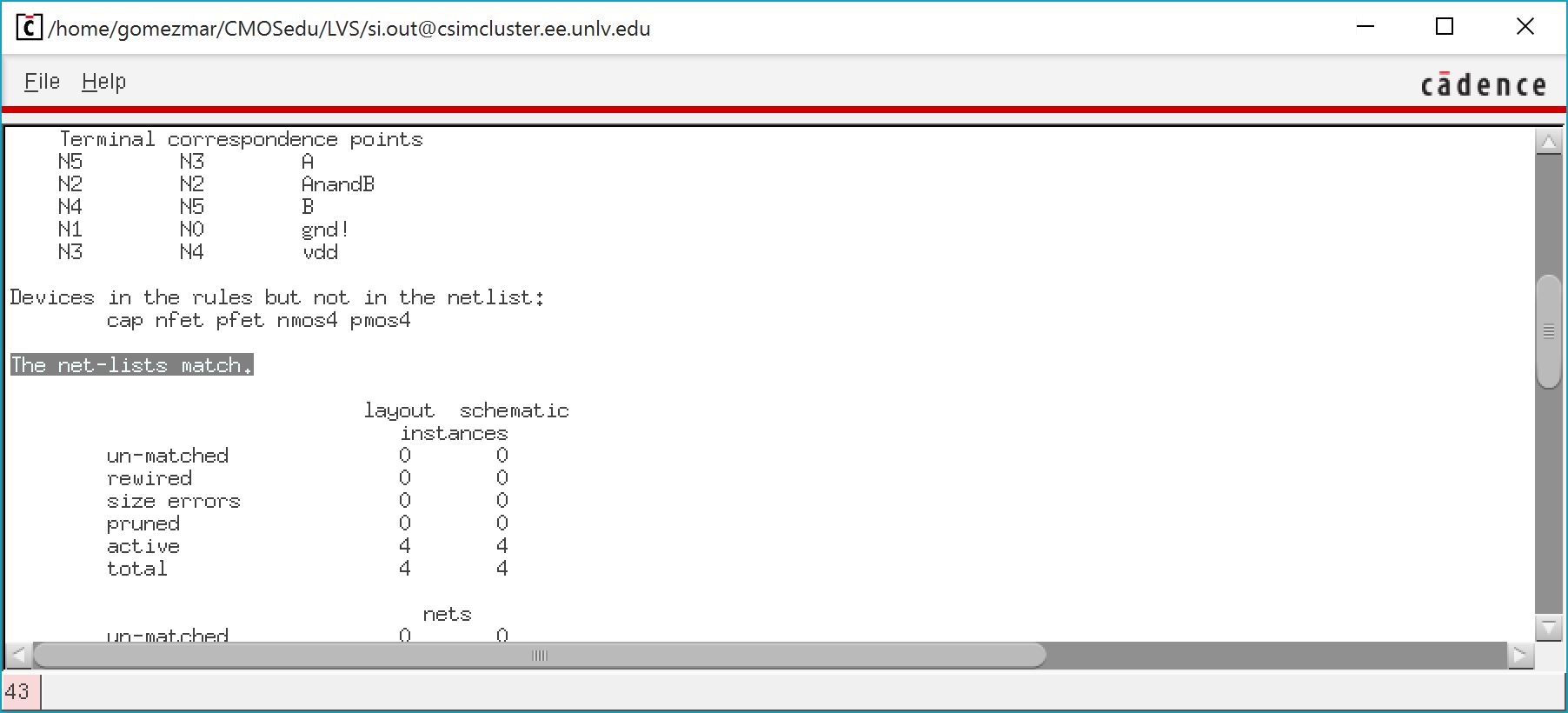
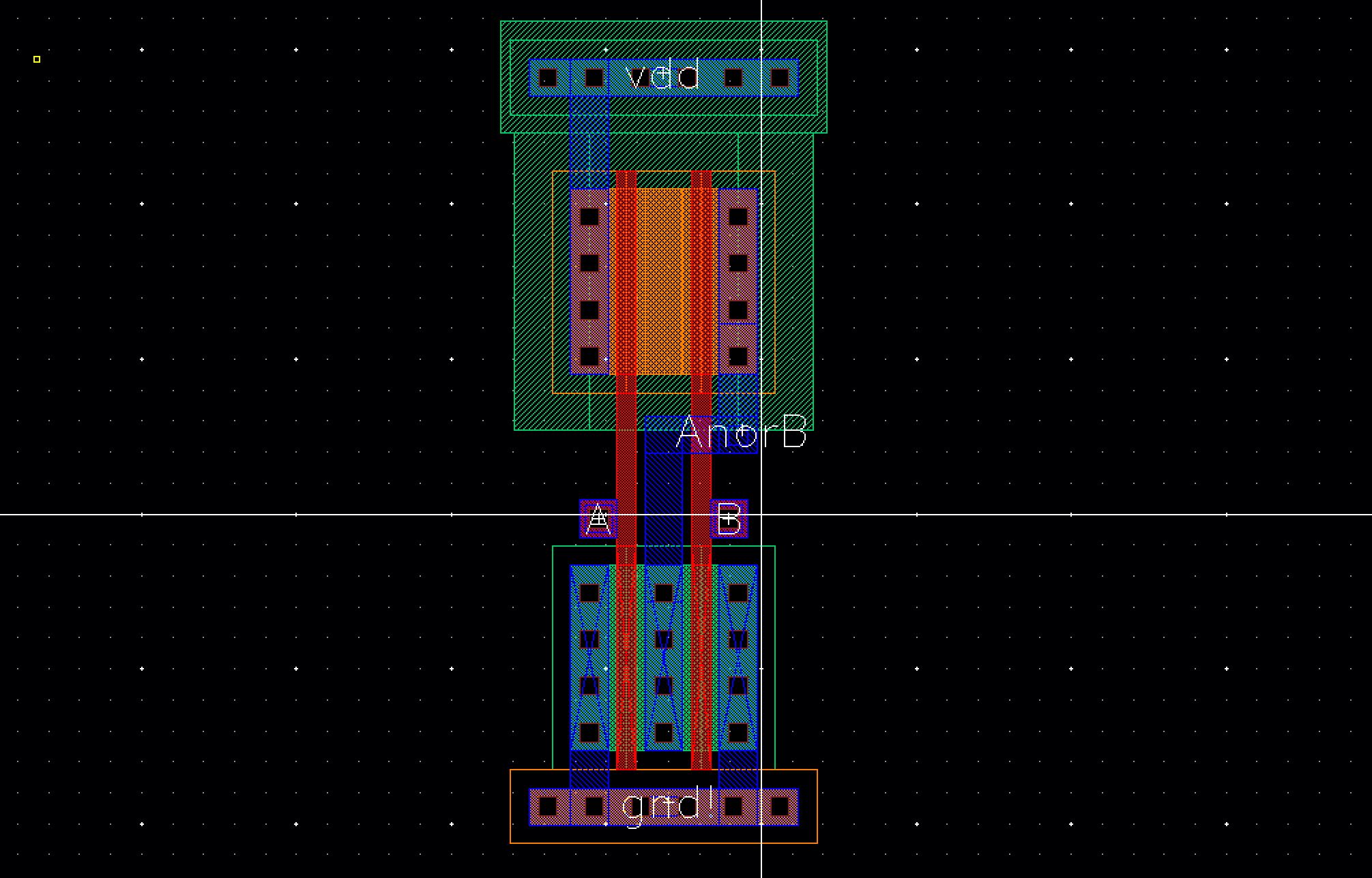
- The layout was also created for the NOR gate.
- A DRC check was then performed on the layout to make sure there were no errors.
- An LVS was also performed to ensure the layout matched the schematic.


- To ensure there were no problems with the layouts a simulation was performed using the extracted view.
- The results obtained were the same as when the simulation was performed using the schematic further proving that the layout is correct.

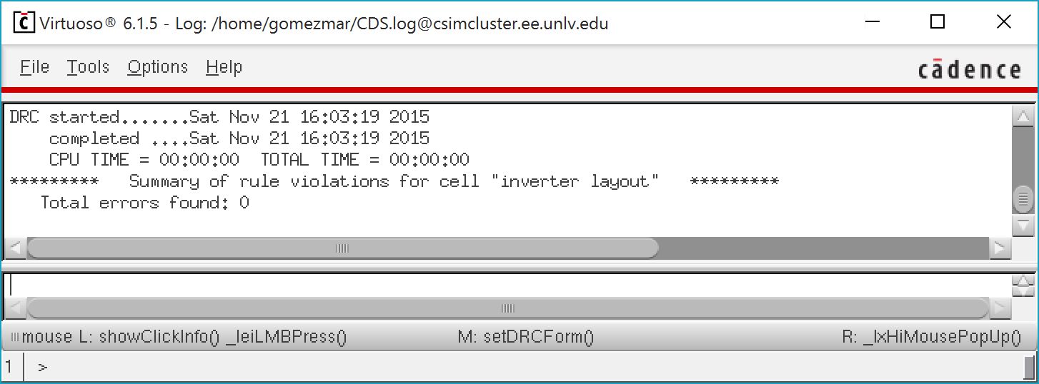
- A layout was then created for the 12u/6u invrter.
- A DRC check was then performed on the layout to make sure there were no errors.
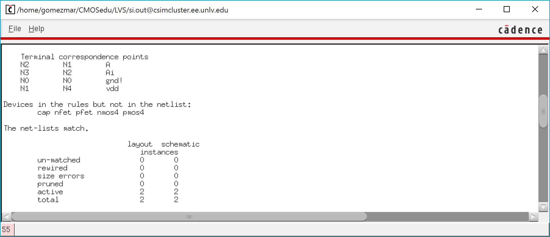
- An LVS was also performed to ensure the layout matched the schematic.
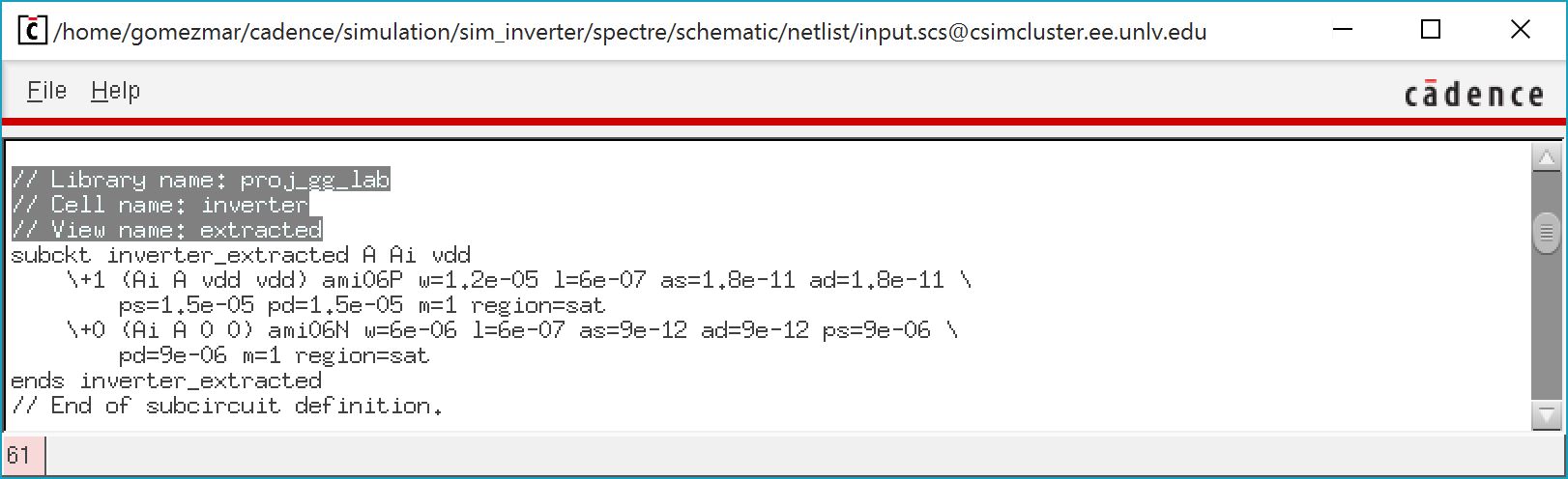
- To ensure there were no problems with the layout a simulation was performed using the extracted view.
- The results obtained were the same as when the simulation was performed using the schematic further proving that the layout is correct.

- A layout was then created for the NMOS.
- A DRC check was then performed on the layout to make sure there were no errors.
- An LVS was also performed to ensure the layout matched the schematic.


- To ensure there were no problems with the layout a simulation was performed using the extracted view.
- The results obtained were the same as when the simulation was performed using the schematic further proving that the layout is correct.

- A layout was then created for the PMOS.

- A DRC check was then performed on the layout to make sure there were no errors.
- An LVS was also performed to ensure the layout matched the schematic.

- To ensure there were no problems with the layout a simulation was performed using the extracted view.
- The results obtained were the same as when the simulation was performed using the schematic further proving that the layout is correct.

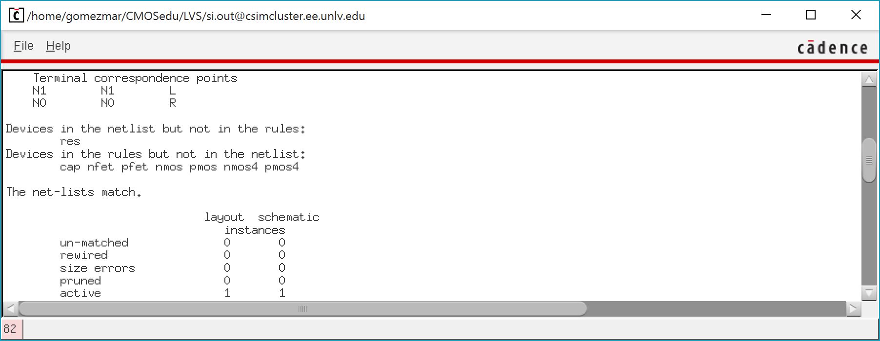
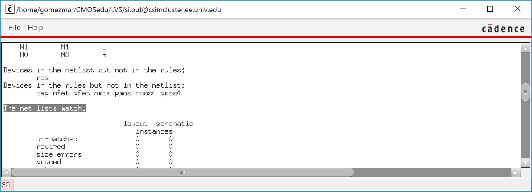
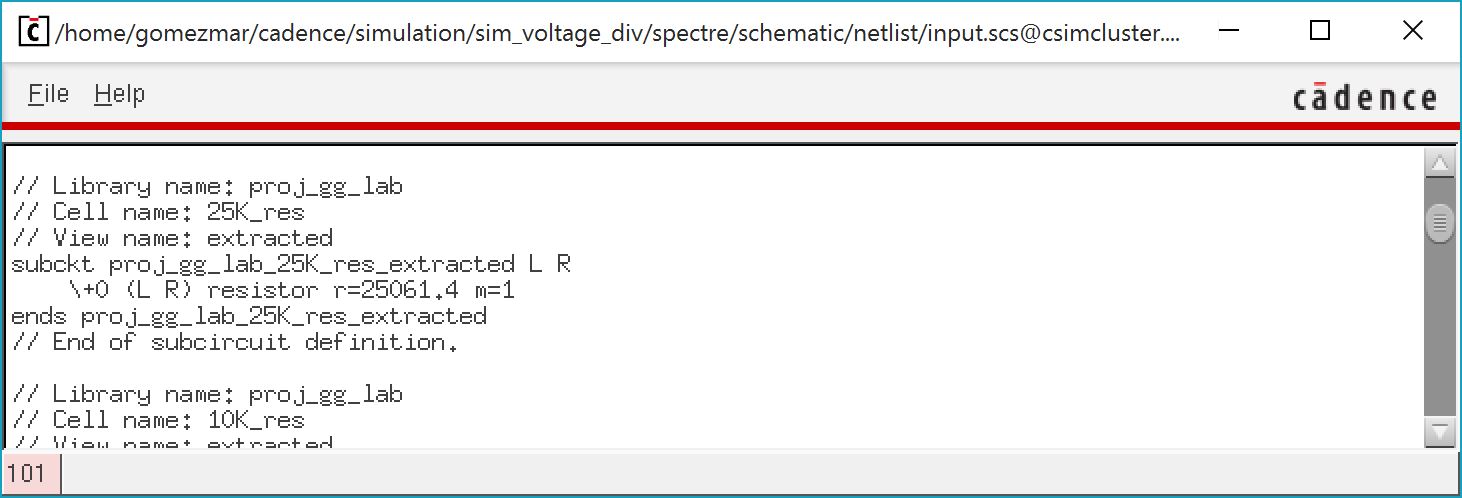
- A layout was then created for the 25K resistor using n-well.
- A DRC check was then performed on the layout to make sure there were no errors.
- An LVS was also performed to ensure the layout matched the schematic.

- To ensure there were no problems with the layout a simulation was performed using the extracted view.
- The results obtained were the same as when the simulation was performed using the schematic further proving that the layout is correct.

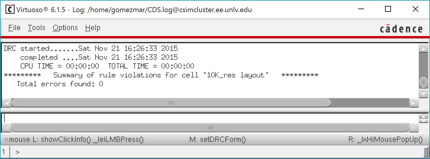
- A layout was then created for the 25K resistor using n-well.

- A DRC check was then performed on the layout to make sure there were no errors.
- An LVS was also performed to ensure the layout matched the schematic.
- To ensure there were no problems with the layout a simulation was performed using the extracted view.
- The results obtained were the same as when the simulation was performed using the schematic further proving that the layout is correct.
- All of the files for this lab can be found here: proj_gg_lab.zip