Lab description
The purpose of this lab was to layout and simulate an inverter.
Lab Report
12u/6u Inverter
- First a schematic for the 12u/6u inverter was created.
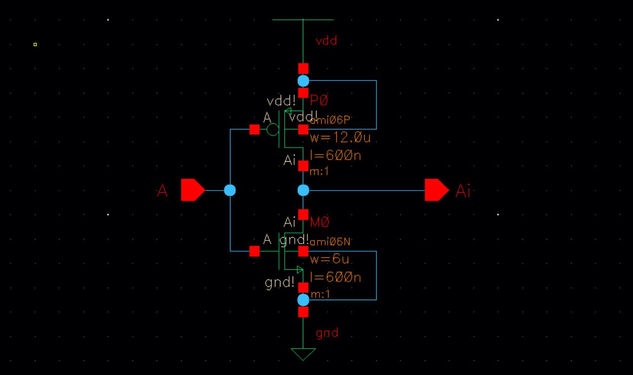
- A symbol was created from the above schematic with some text indicating the type of inverter.

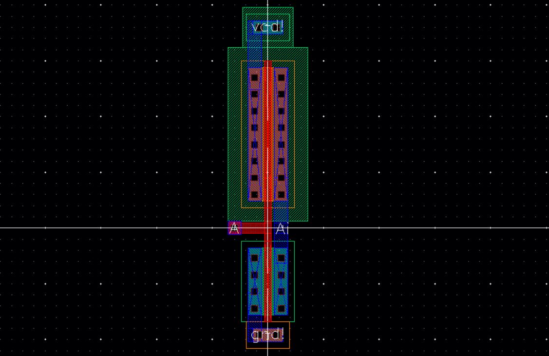
- Then a layout for the inverter was created to match the schematic.
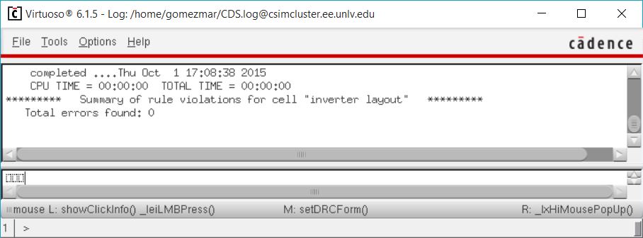
- A DRC check was performed to be sure there were no errors on the layout.
- Then an LVS was performed between the schematic and extracted layout and the net-lists were found to match.

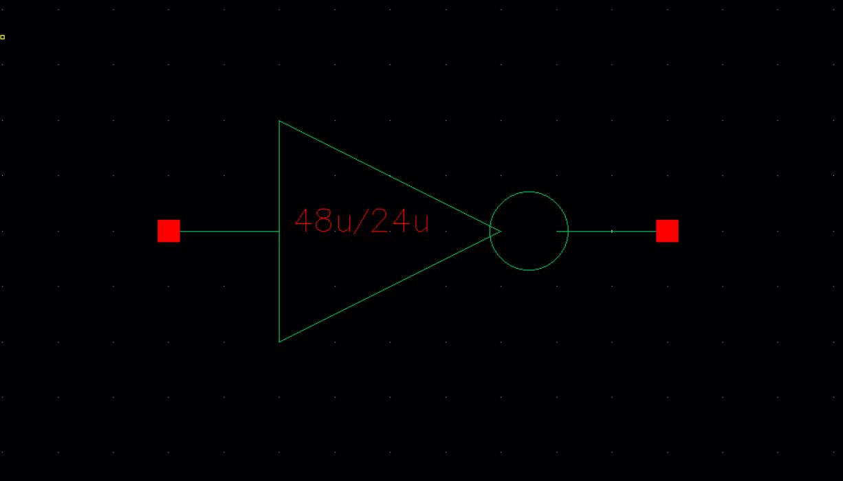
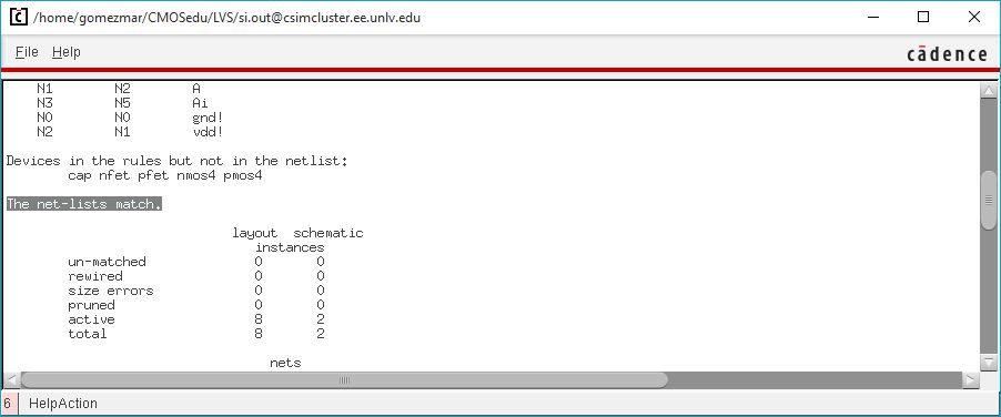
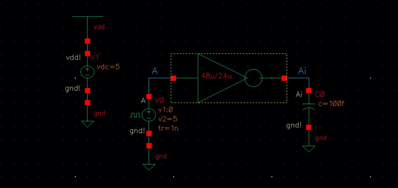
48u/24u Inverter
- A schematic for the 48u/24u inverter was created.
- The schematic from the 12u/6u inverter was copied but the multiplier for the MOSFETS was changed to 4.
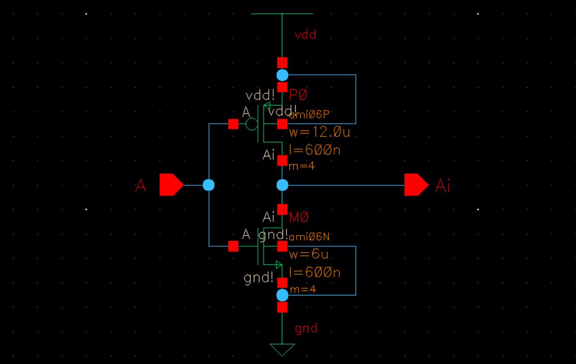
- A symbol was created from the above schematic with some text indicating the type of inverter.
- Then a layout for the inverter was created to match the schematic.
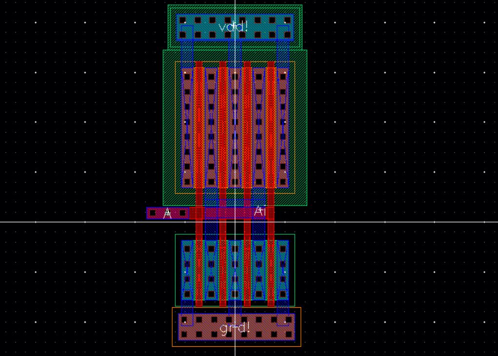
- A DRC check was performed to be sure there were no errors on the layout.

- Then an LVS was performed between the schematic and extracted layout and the net-lists were found to match.
Inverter simulations
- Then the inverters that were created were simulated driving a capacitive load.
- We started by simulating the operation of the 12u/6u inverter.

- With a load of 100fF the resulting simulation can be seen below.
- With a load of 1pF it takes longer for the capacitor to charge and dischrage so the output takes longer to change.

- With a load of 10pF it takes even longer for the capacitor to charge and discharge so the output takes longer to change.
- Therefore the amount of time between input changes was chnaged in order to see the full operation of the inverter.
- With a load of 100pF it takes even longer for the capacitor to charge and discharge so the output takes longer to change.
- Therefore the amount of time between input changes was chnaged in order to see the full operation of the inverter.

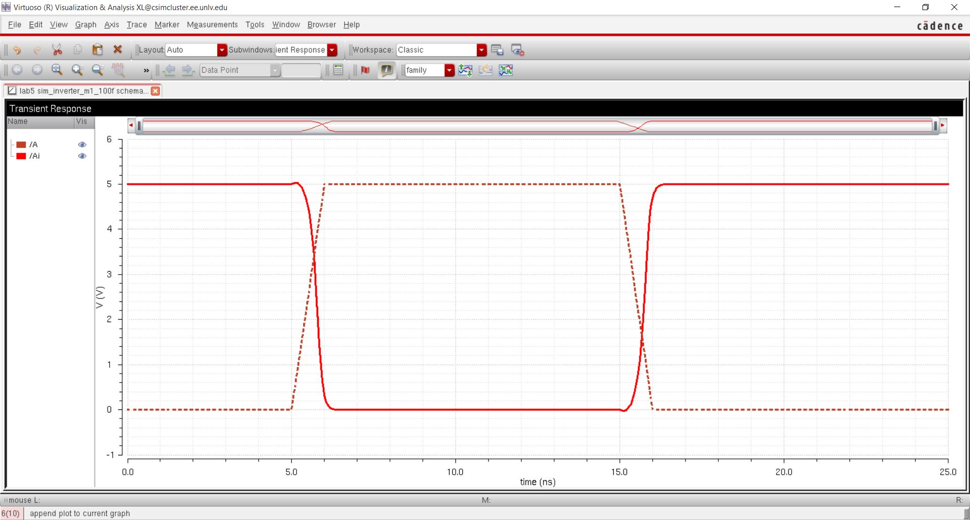
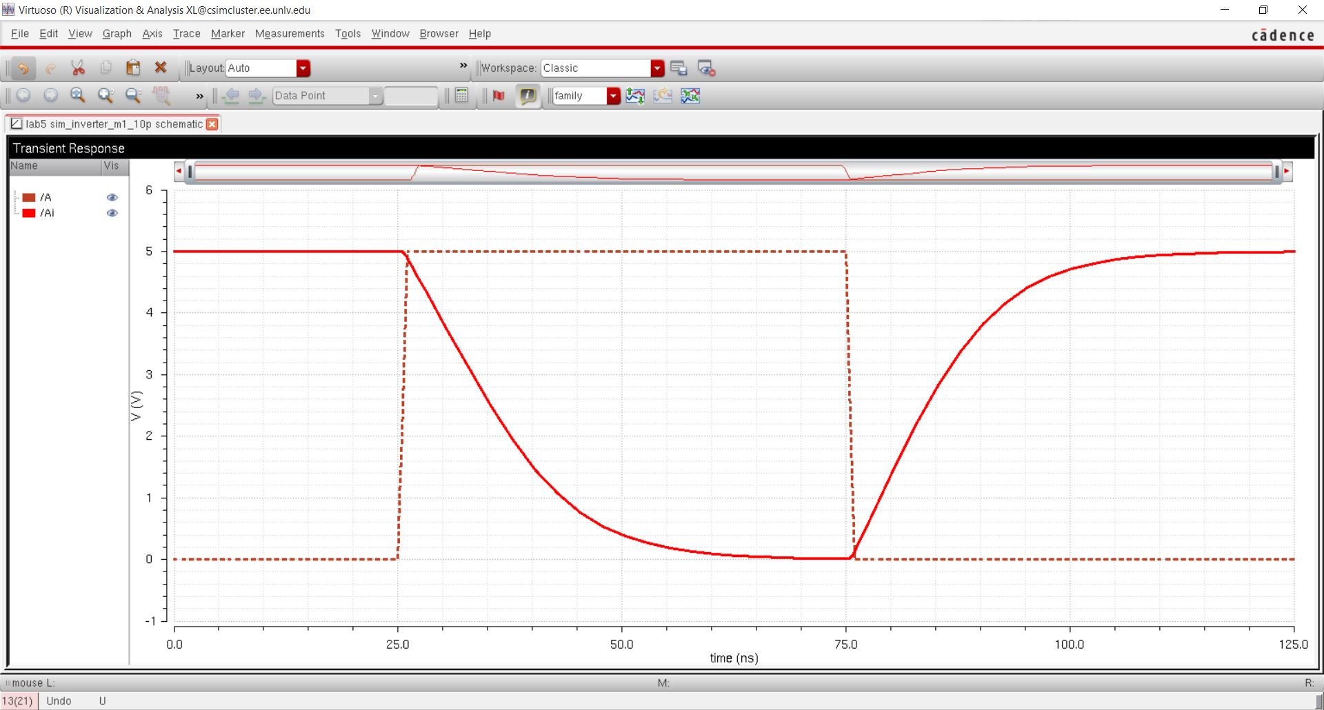
- Then the operation of the 48u/24u inverter was simulated.
- With a load of 100fF the resulting simulation can be seen below.

- With a load of 1pF it takes longer for the capacitor to charge and dischrage so the output takes longer to change.

- With a load of 10pF it takes longer for the capacitor to charge and dischrage so the output takes longer to change.
- Here we did not need to change the amount of time between changes in the input like we did with the 12u/6u inverter with the same load.
- Therefore it can be seen that with the bigger inverter the capacitor charges and discharges faster.

- With a load of 100pF it takes even longer for the capacitor to charge and discharge so the output takes longer to change.
- Therefore the amount of time between input changes was chnaged in order to see the full operation of the inverter.

Using UltraSim
- Then the above simulations were performed using UltraSim (Cadence's fast SPICE simulator).
- The results obtained were really similar to the ones obtained previously, but small changes can be seen.
- A comparison between the simulations can be seen below, the biggest differences can be seen when the output is going from changing to being still.
- It can be seen that the changes take longer to be visible in UltraSim as it is not as accurate.

- All of the files for this lab can be found here: lab5.zip