Lab description
The purpose of this lab was to layout MOSFETS and simulate their IV characteristics.
Lab Report
Simulation 1
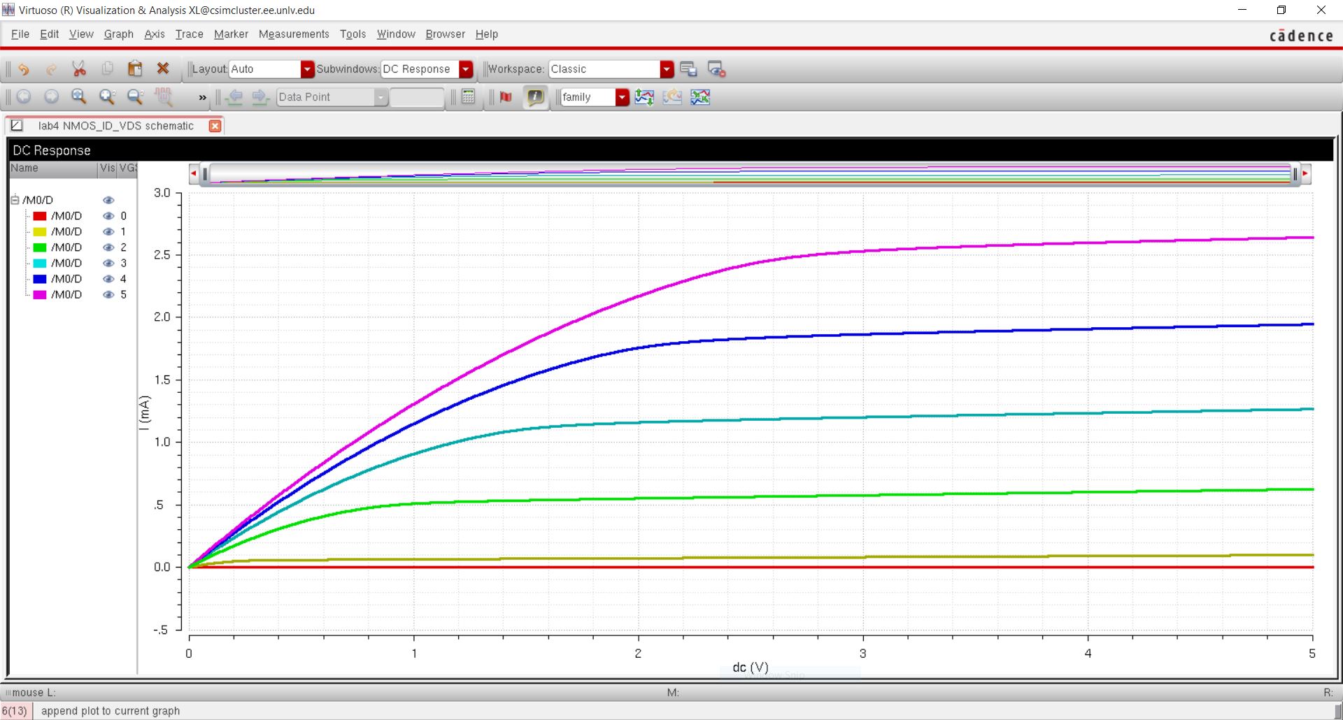
- Simulating ID v. VDS of an NMOS device for VGS varying from 0 to 5 V in 1 V steps while VDS varies from 0 to 5 V in 1 mV steps.

Simulation 2
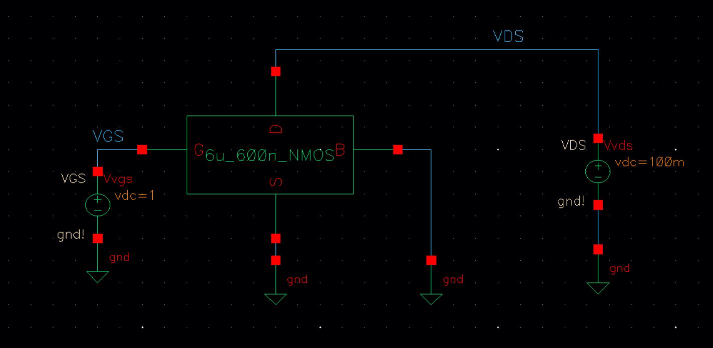
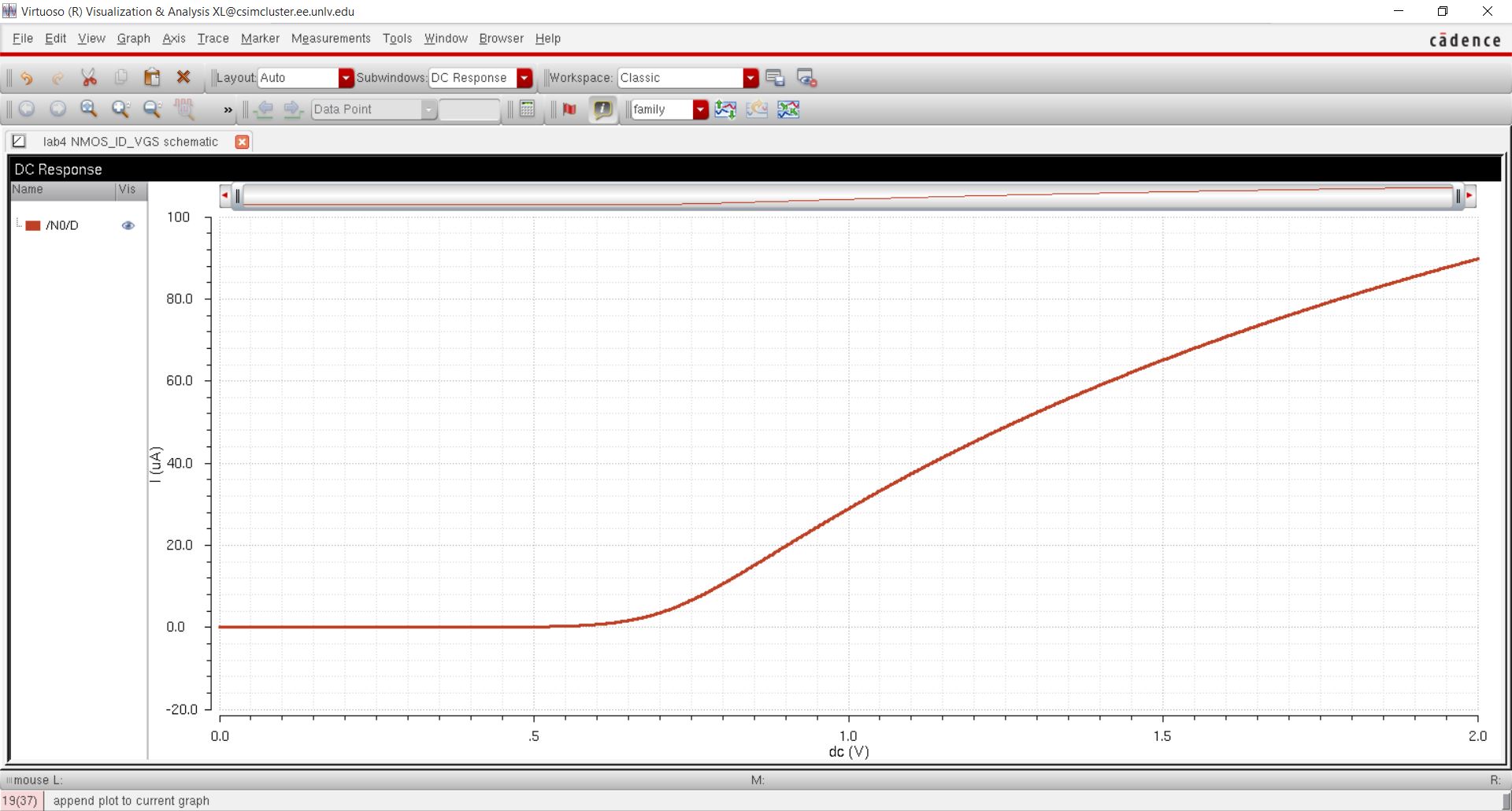
- Simulating ID v. VGS of an NMOS device for VDS = 100 mV where VGS varies from 0 to 2 V in 1 mV steps.
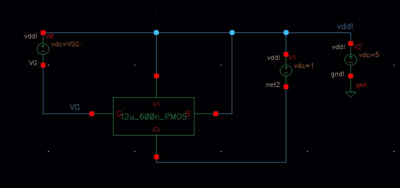
Simulation 3
- Simulating ID v. VSD (note VSD not VDS) of a PMOS device for VSG (not VGS) varying from 0 to 5 V in 1 V steps while VSD varies from 0 to 5 V in 1 mV steps.

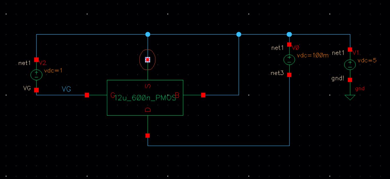
Simulation 4
- Simulating ID v. VSG of a PMOS device for VSD = 100 mV where VSG varies from 0 to 2 V in 1 mV steps.

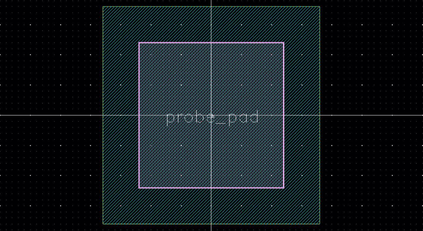
Layout of Probe Pad
- We had to start by creating the layout for the probe pads to be used on our design.
- These are created to be smaller than bond pads as the size needed for them has to only be larger than 20 um.
- The layout can be seen below.
- Then I create a schematic for the bond pad, using a noConn to ensure there are no warnings.

- Then a symbol was created from the schematic so it can be used on the MOSFET schematic.

Creating the NMOS
- Then I created a schematic for the NMOS device.
- The probe pads created earlier were used to connect to each of the terminals.

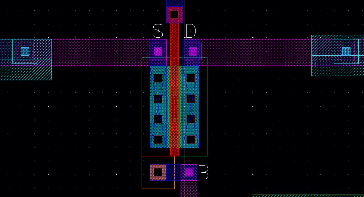
- A layout was then created for the NMOS.
- Instances of the probe pad layout were added to our layout and were connected using the 3 metal layers and VIAs.

- A close up of the NMOS layout and its connections can be seen below.
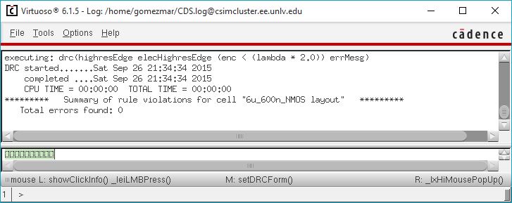
- Then a DRC check was performed on the layout to make sure there were no errors.
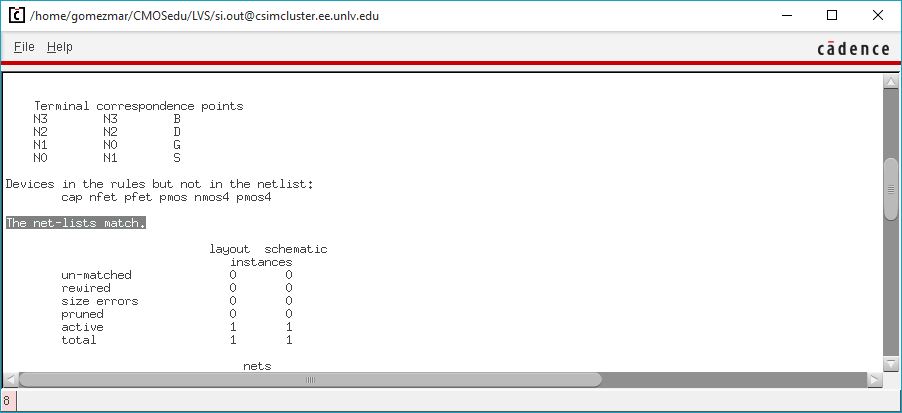
- The layoout was then extracted and a LVS was performed, the schematic and the layout matched.
- Once I was sure my design was correct I created a symbol from the schematic.

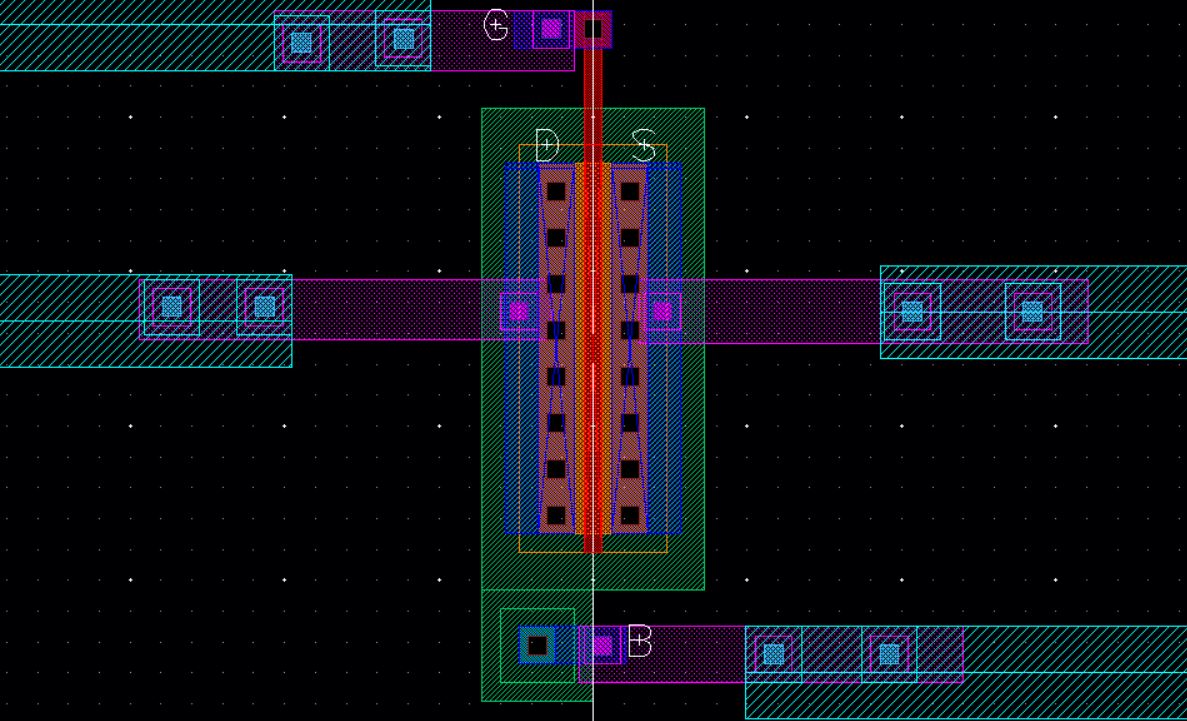
Creating the PMOS
- Then I created a schematic for the PMOS device.
- The probe pads created earlier were used to connect to each of the terminals.
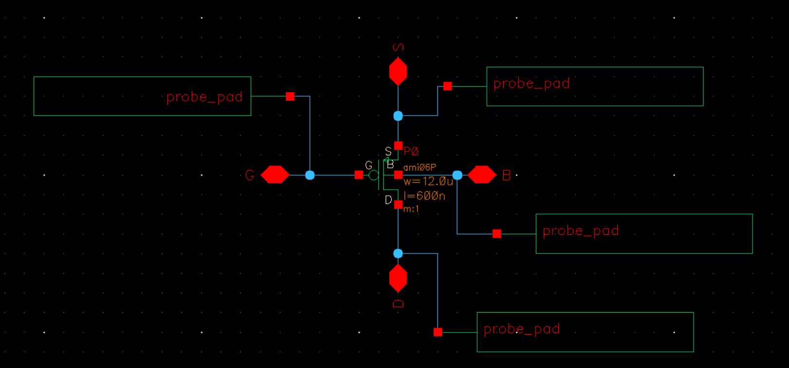
- A layout was then created for the PMOS.
- Instances of the probe pad layout were added to our layout and were connected using the 3 metal layers and VIAs.
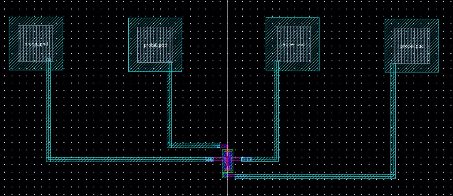
- A close up of the PMOS layout and its connections can be seen below.
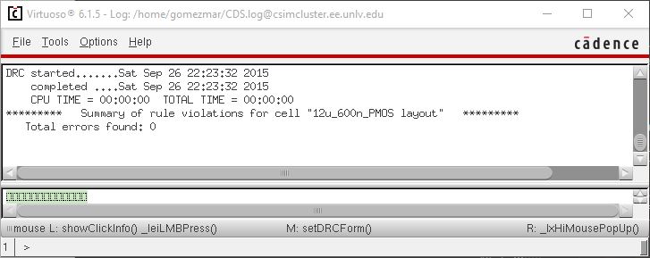
- Then a DRC check was performed on the layout to make sure there were no errors.
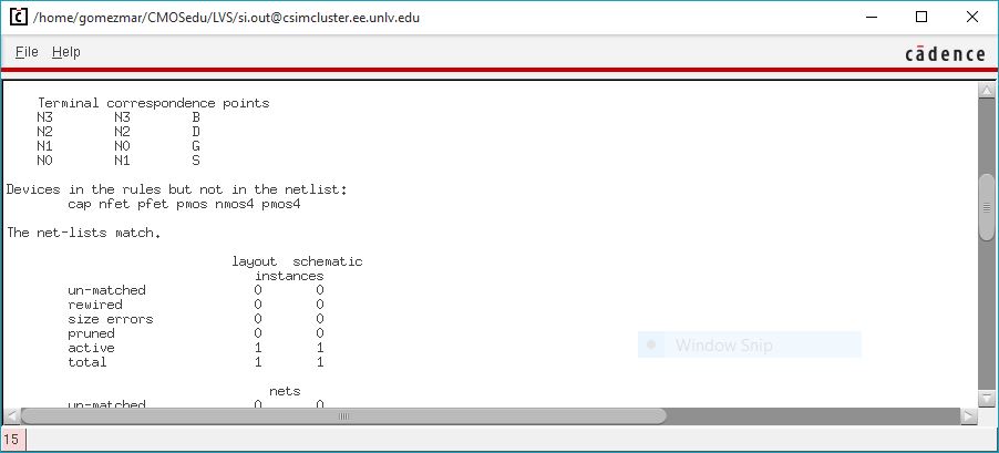
- The layoout was then extracted and a LVS was performed, the schematic and the layout matched.
- Once I was sure my design was correct I created a symbol from the schematic.