Lab 6 - ECE 421L 

Authored by Chris Givens

givensc2@unlv.nevada.edu

10/19/2015


The purpose of this lab is to start applying all the skills gained in cadence to make a real digital circuit. 6u x .6u NMOS and PMOS will be used to create NAND and XOR gates which will ultimately be put together to create a 2-input full adder.

First, we must create the basic NAND and XOR gates that will be used. Cadence doesn't check the validity of the layout, only of the schematic so we must simulate the gate in schematic form.

Below are the schematics of the NAND gate and XOR gate respectively.

NANDschem.JPG


XORschem.JPG


Now symbols for both of the gates can be created. I copied the stock symbol for both gastes from cadence into the cymbol vies for these gates. The label wieh my initials shows that it is indeed a new symbol.


NANDsym.JPG


XORsym.JPG


Now that we have these symbols we can put them into a schematic and simulate their functionality. Note that vdd must be supplied or the gates will not function properly.


GateSchem.JPG


Below is the pulse for the "A" input:

GatePulse.JPG


And the settings for the "B" input:

GateBPulse.JPG


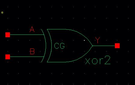
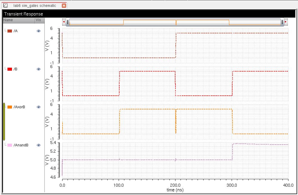
Finally, the output of the gates:

Gate%20output.JPG


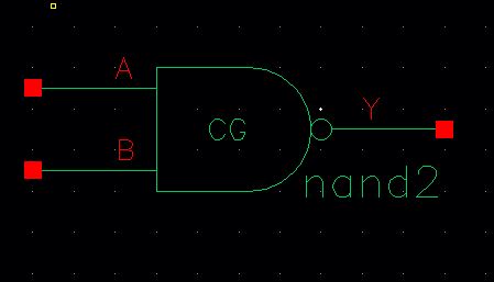
Now that we know the output of the gates we can create the layout, which Cadence will check against these schematics. The NAND gate is simple as it contains 2 MOSFETS connected in series. The inputs are labeled "A" and "B" and the output is labeled "Y."

NANDlayout.JPG


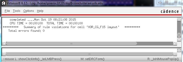
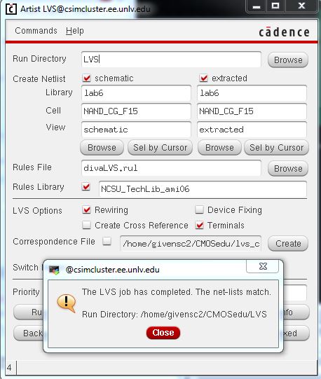
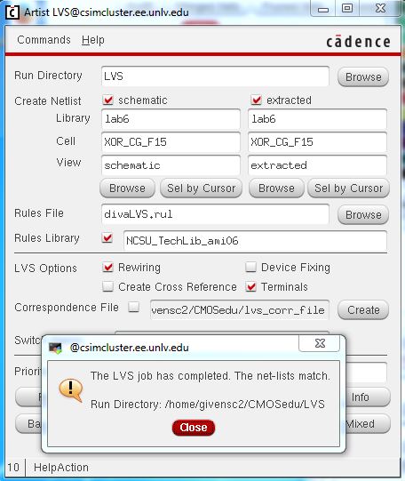
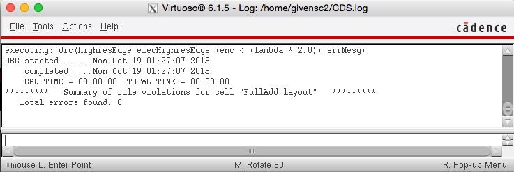
DRC, extract, and LVS the Layout:

XORdrc.JPG


NANDlvs.JPG


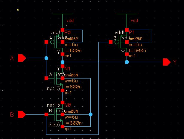
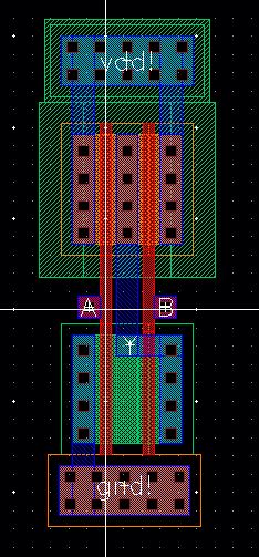
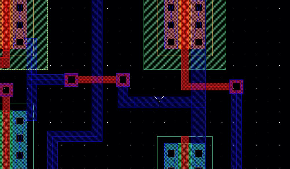
The XOR gate is more complicated. All routing is done on the poly1 and metal1 layers. The metal2 layer is saved for later use.


XORlayout.JPG


Looking back, this design is flawed. The p-substrate that acts as the body for the NMOS is slightly resistive and the two NMOS located in the middle of the layout, not near the grounded ptap will likely have noise issues. But the layout passed DRC and LVS.


XORdrc.JPGXORlvs.JPG


Below is a closeup of the inputs of the XOR gate. Notice they are attached to the body of the MOSFETs as depicted in the schematic.


XORinputs.JPG


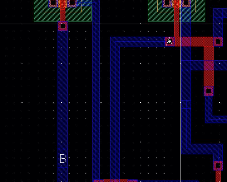
And the output is between the source and drain of the set of 4 NMOSs and PMOSs.


XORout.JPG


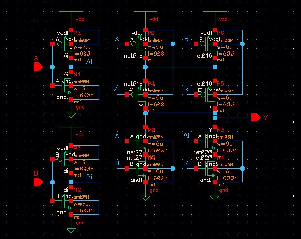
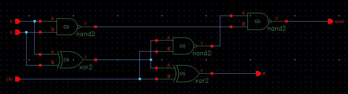
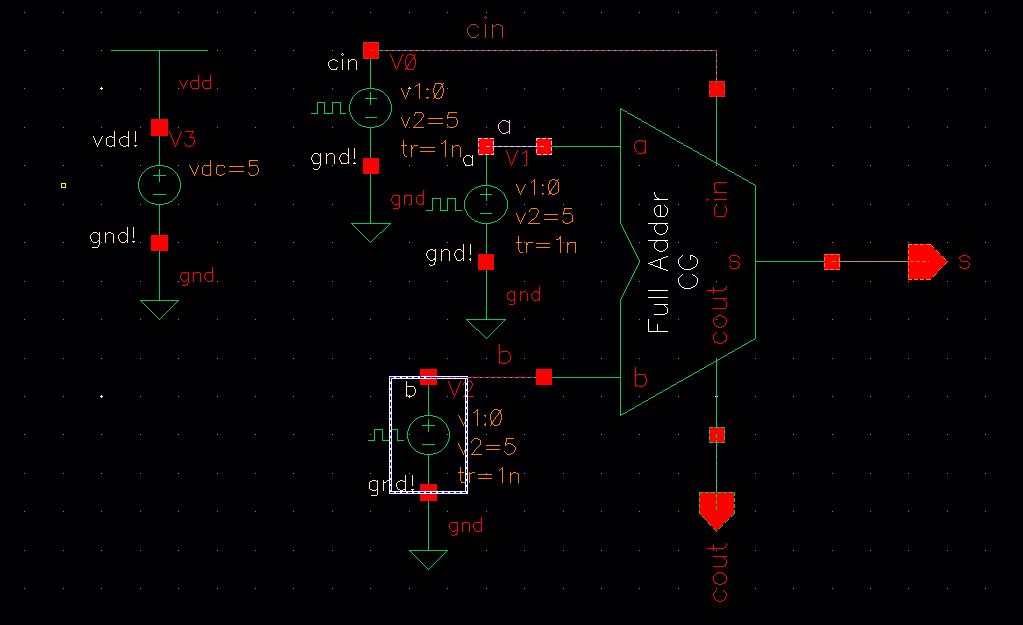
Now to put it all together. Below is the schematic for the 2-bit Full Adder using the symbols created earlier:


FullAdd.JPG


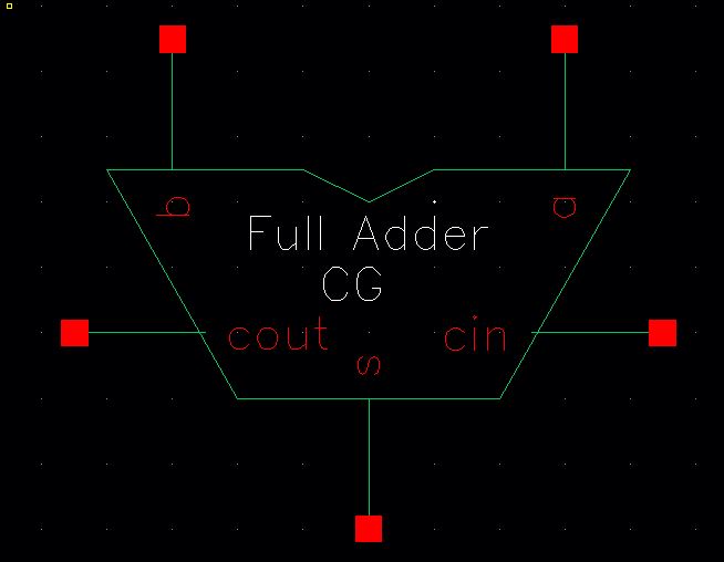
And the symbol for the Full Adder:


FAsym.JPG


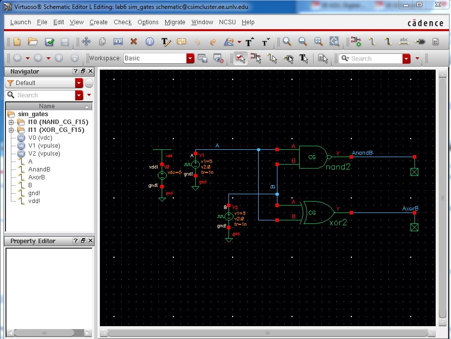
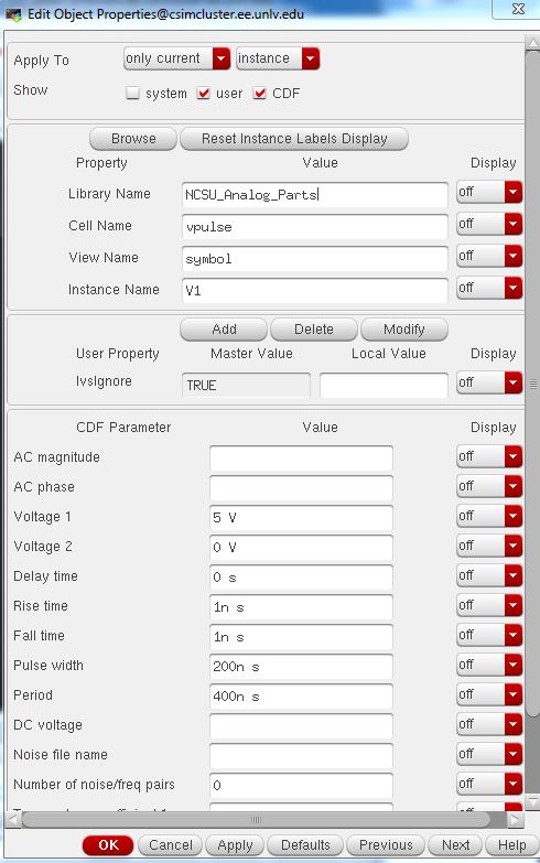
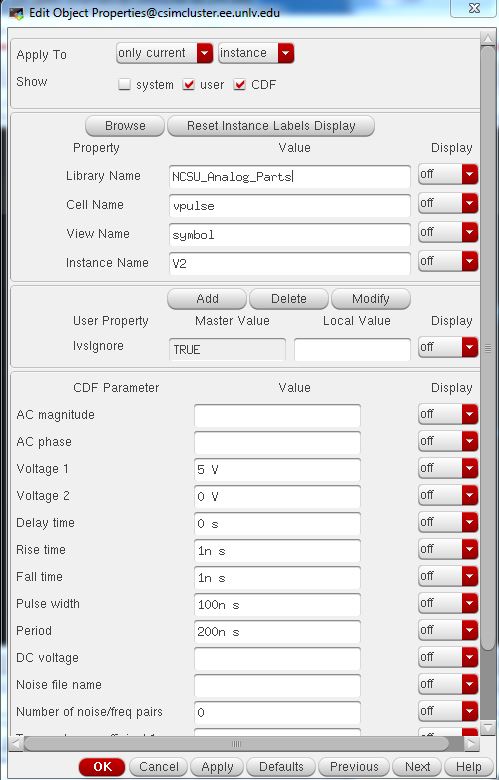
Let's simulate the full adder using the symbol (and schematic) from above. Once again, vdd must be present or the circuit won't run properly.
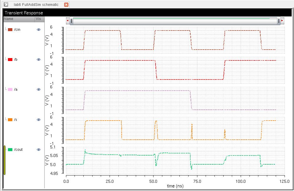
 

FAschem.JPG


Output:


FAout.JPG


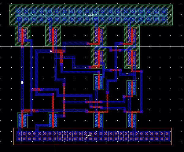
Finally, based off of the Full Adder schematic, layout the circuit using the gate layouts created previously:


FAlayoutNAND.JPG


Notice the 3 NAND gates circled in red. The routing and pins for the unified circuit are placed on metal2 to differentiate the levels of routing.


The Full Adder passed DRC:

FAdrc.jpg


Hower getting it to pass LVS was a little more tricky:


LVSfail.JPG 


Troubleshooting LVS seems to be the hardest part of the process. The outputfile shows that the terminals and nets don't match.


LVSout.JPG


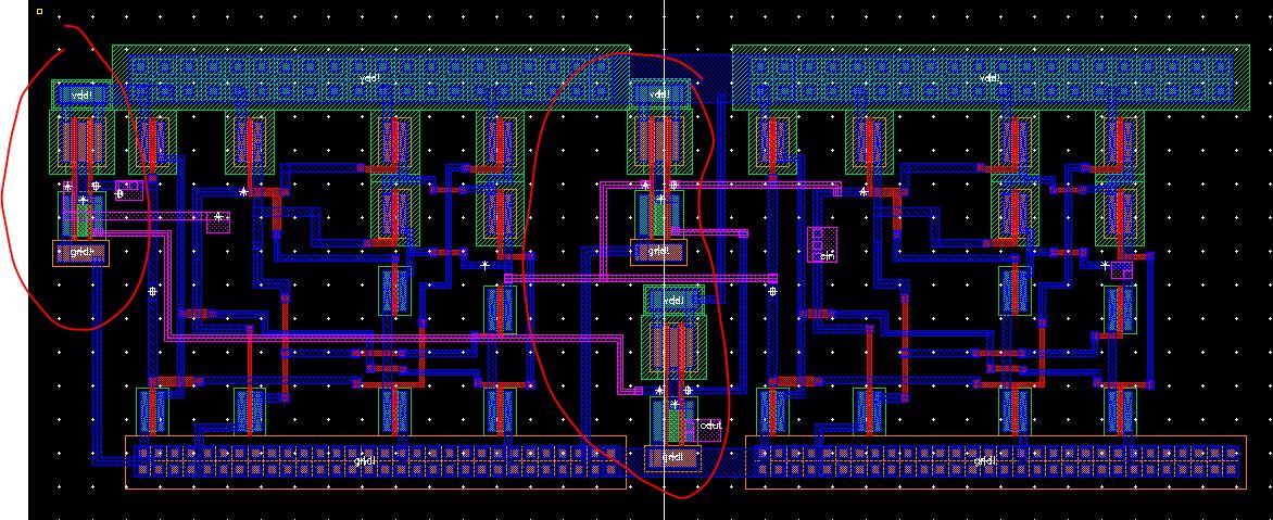
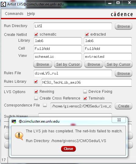
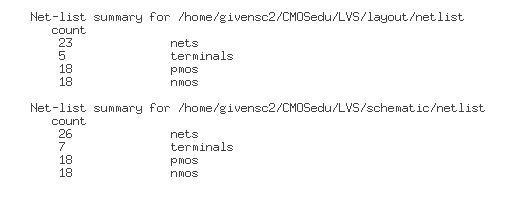
I tied the ground and vdd of all the NAND gates to their respective supply rails. I doubt this had anything to do with th LVS problem, as it still wouldn't pass LVS. The problem seemd to lie in the middle of the circuit. "cin" and "s" were routed incorrectly.


Success!

LVS.JPG