Lab 5- ECE 421L
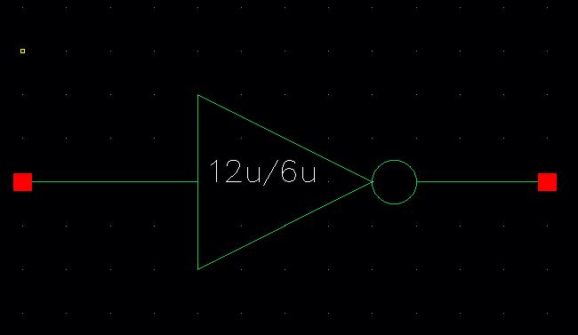
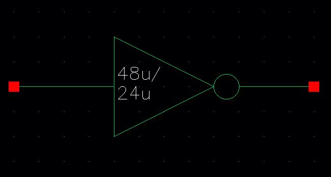
Create a symbol for each inverter.
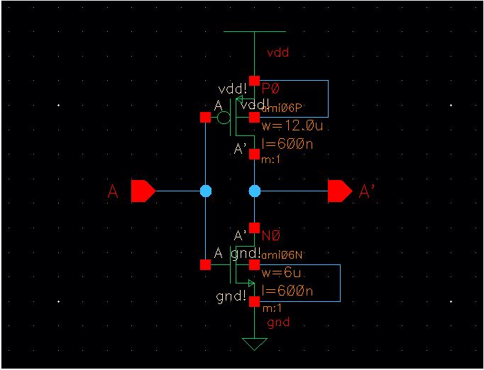
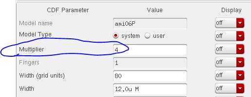
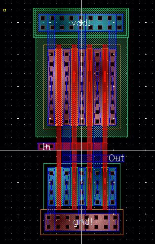
Now, for the layout. Use the stock nmos4 and pmos4 transistors to layout the inverter from the schematic. Do this for each size inverter. Note, the names A, A' were changed in the 4x inverter during troubleshooting of LVS errors. The names don't matter as long as they make sense and are associated with pins the schematic.
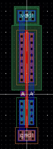
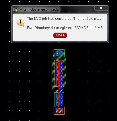
DRC and extract the layouts. LVS the layout to check that the netlists match.
Now for the fun part: making the circuit come to life.
Use the symbol of the invertor in the circuit below. Note the value of the capacitive load. We will be parametering that load to check the output under a varying load.
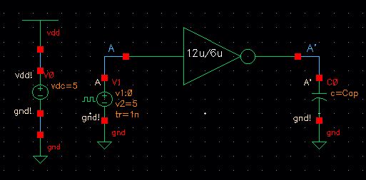
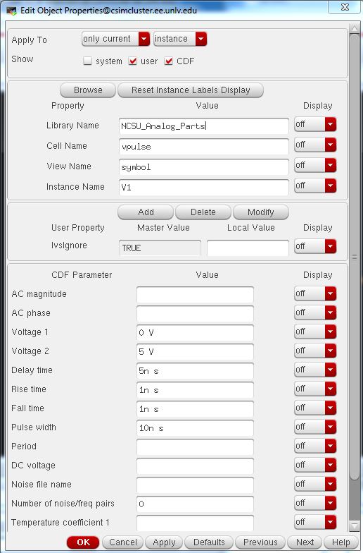
The pulse source should have the following parameters:
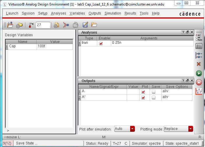
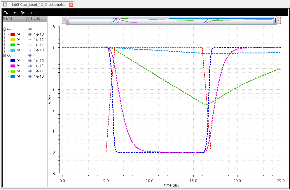
Launch ADE L and set up a transient analysis for 25ns.
The outputs will be A and A'. The design variable will the capacitive load.
Click on Tools > Parametric Analysis.
The capacitive loads required for modeling are 100fF, 1pF, 10pF, and
100pF. We will use the decade parametric sweep for this simulation.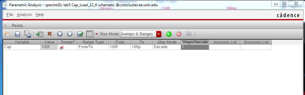
Run the simulation by hitting the green circle. The output should look like this:
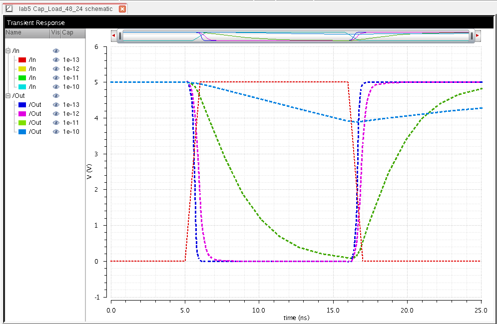
The red dotted line is the input. The dark blue line is the output for the 100fF load and the lighter blue line is the output for the 100pF load. The load greatly varies the output of the circuit.
Since we are doing a transient analysis we can use UltraSim which generates faster at the expense of accuracy. UltraSim didn't seem to like the naming convention A' so the labels were changed to "In" and "Out."
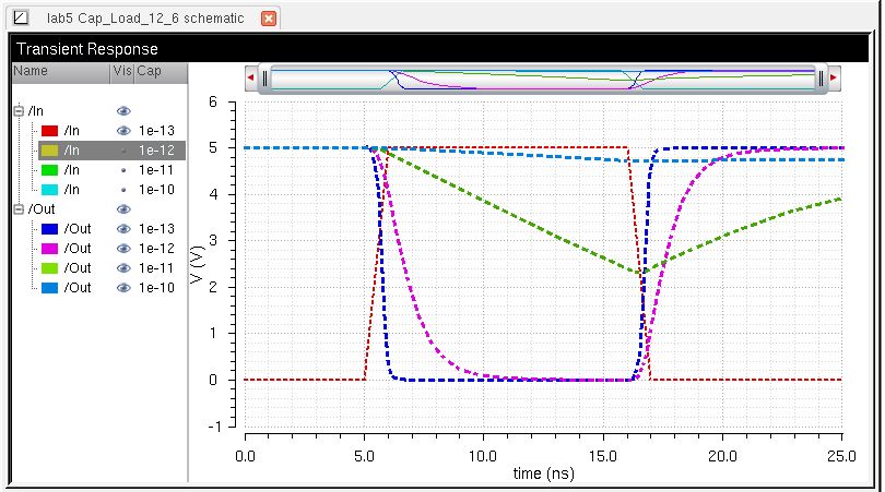
Look at the difference in the outputs of the 1p, 10p, and 100p loads. The results are very different.
Repeat the simulations (both Spectre and UltraSim) for the 4x inverter.
Spectre:
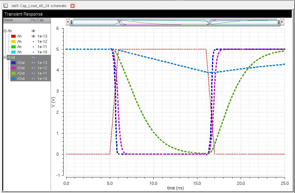
UnltraSim:
While the accuracy of UltraSim is minimal, the trend of the effects of the capacitive load are still evident. The capacitance greatly effects the output of the circuit.