Lab 4 - ECE 421L
Chris Givens
givesnc2@unlv.nevada.edu
9/28/2015
This
lab is intended to further the understanding and use of Cadence. In
this lab we will simulate parametric DC voltage sweeps in NMOS and PMOS
transistors as well as lay out the devices.
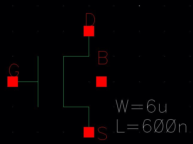
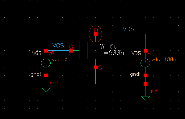
First, we needed to create a symbol for our transistor, the NMOS.
Instantiate a 4-pin generic NMOS, and make the width= 6uM and the length=600nM. Connect pins to each io of the tansistor.
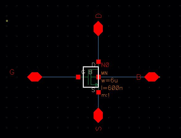
Next, create a symbol for the transistor. Label the dimensions.
Now we can use th NMOS in our schematic to plot the IV curves.
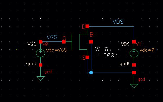
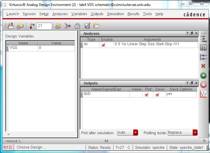
After
the schematic is set, we can plot the IV curves. Make sure that the
voltage for V0 is set to equal VGS, it will be reference in the
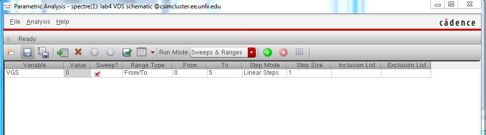
parametric settings. Use the settings below to set up the simulation.
Make sure VGS is set to some random value in the design variables.
We also need to attach the generic NMOS model to the schematic. Click
Setup > Model Libraries. Click on "Click Here to Add Model File,"
then navigate to home/ncsu-cdk-1.6.0beta/models/spectre/standalone/ami06N.m
Click "Ok."
To parameterize the simulation click on Tools > Parametric Analysis. Use the settings below.
Click the green "play" button in the window and what follows is a parameterized IV curve for the MOSFET.
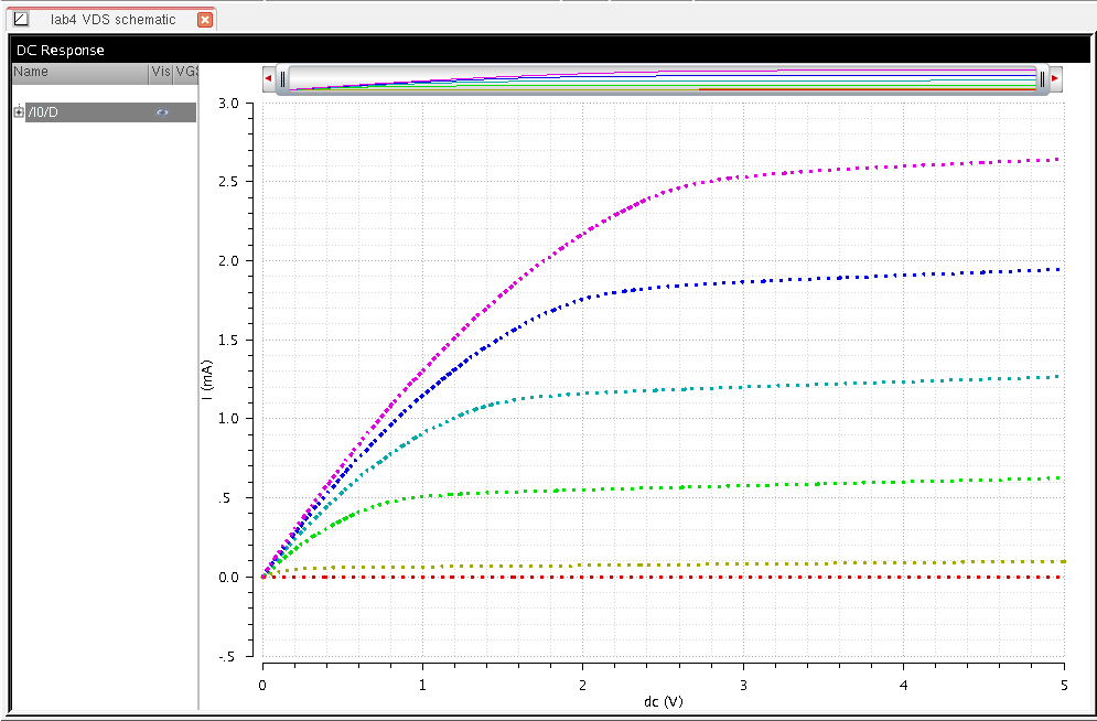
Next,
to plot the IV curve due to the Gate Voltage VGS. Copy the schematic to
a new Cell View and open it. Change V1 to 100mV.
Copy the Spectre_State into the same Cell View and open it.