Lab 3 - ECE 421L
Chris Givens
givensc2@unlv.nevada.edu
9/21/2015
The
focus of this lab is to expand on the previous lab. Using the schematic
and symbol that were designed in the previous lab we will design,
simulate, and layout a 10-bit Digital-to-Analog (DAC) converter.
The
basic component used in this lab is the n-well resistor. A 10k-Ohm
resistance was mandated in the lab. To create this the MOSIS rules need
to be obeyed as well as the physical properties of the materials used
in the process.
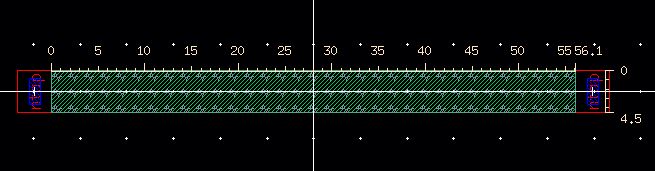
MOSIS
requires a 12 lambda (or 3.6um) width for the n-well and the sheet
resistance is 800 Ohms/square (3.6um x 3.6um if using the minimum
width). Thus, the length must be about 12.5 x the width for a 10k-Ohm
resistance. A width of 4.5um was used for the width, which will give us
a required length of
Due
to snap spacing of Cadence, all blocks must be divisible by .15 um, so
the length is set a little bit over the required length to 56.1um.
Below is the finished 10k-Ohm resistor showing the dimensions used.
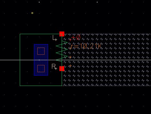
Below is the actual resistance of the resistor that was drafted.
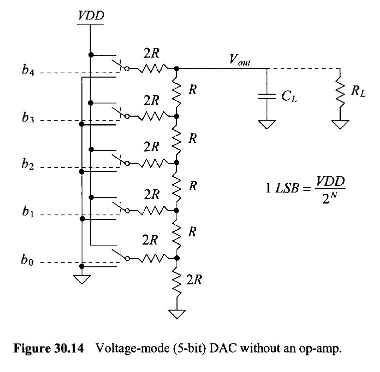
The design used for the DAC is the R-2R topology displayed below.
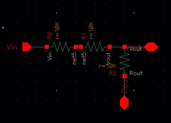
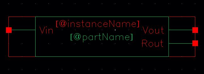
This leads to a schematic for one bit (which was designed in the previous lab):
And the symbol for the scematic:
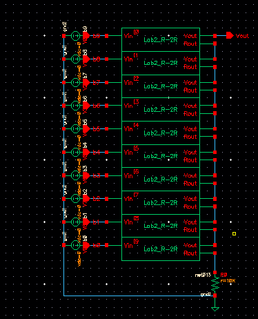
This symbol was used for the schematic of the 10-bit DAC:
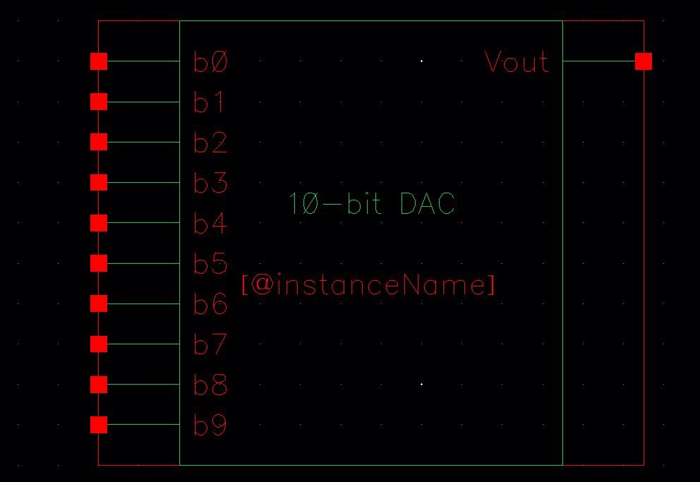
And was used to create a symbol for the 10-bit DAC:
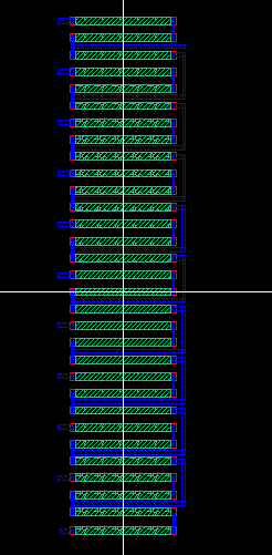
And the layout for the device:
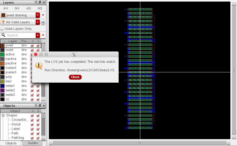
No errors!
Zipped Files
Back to Labs