Project - EE 421L Fall 2015
Zip folder containing Proj files found here
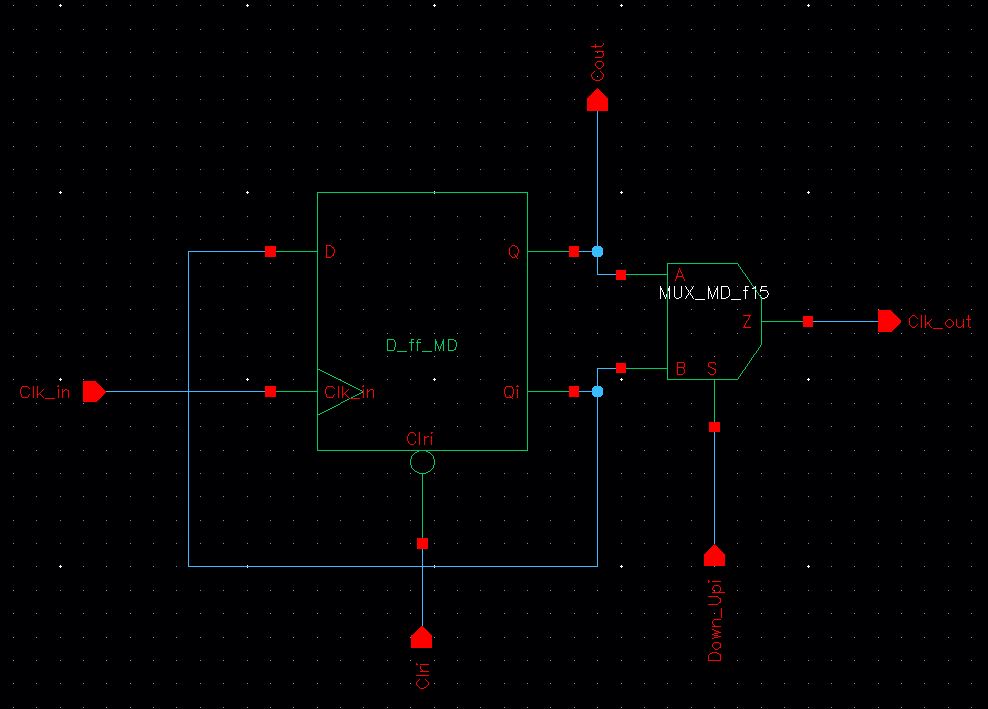
1. Design of an 8-bit resettable (input "clear") up/down counter. The outputs of your counter should be buffered before connecting to a pad. The 8 bit up/ counter has 8 stages, each comprising of a D flip flop with clear and a 2 to 1 multiplexer to select the up/down operation (one bit up/down counter). First stage is directly connected to the clock signal, the other 7 respond after additional delays. For example, stage 2 will change every 2 clock cycles, stage 3 every 4 clock cycles and so on.
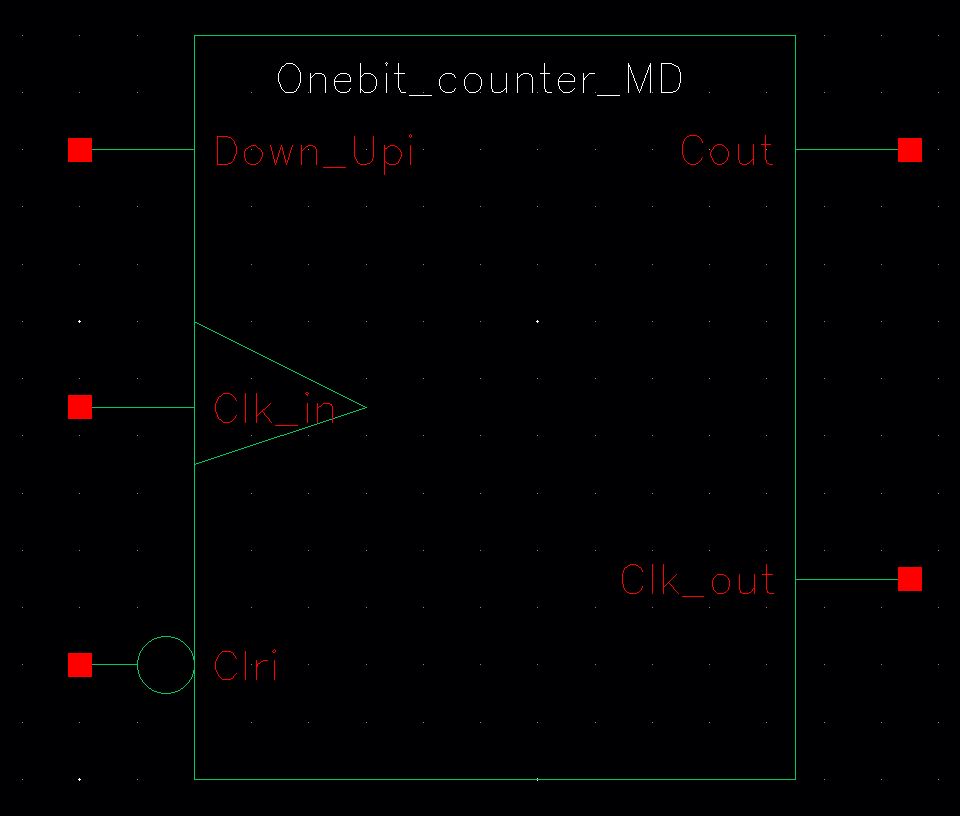
One bit up/down counter.
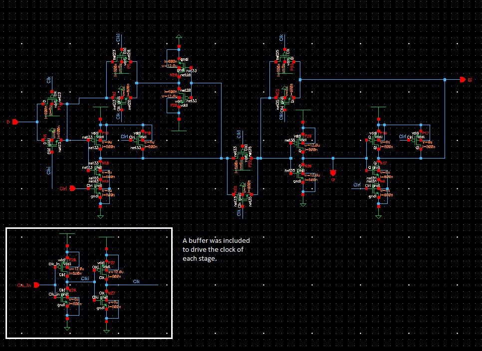
D flip flop with an active low clear. A buffer was included to drive the next stage.
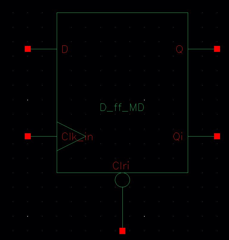
Truth table.
| Reset | D | CLOCK | Q | Qi |
| 1 | 0 | Rising edge | 0 | 1 |
| 1 | 1 | Rising edge | 1 | 0 |
| 0 | X | X | 0 | 1 |
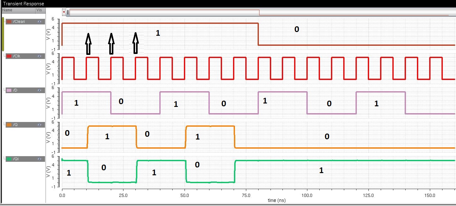
D flip flop simulations
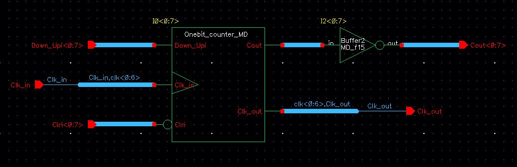
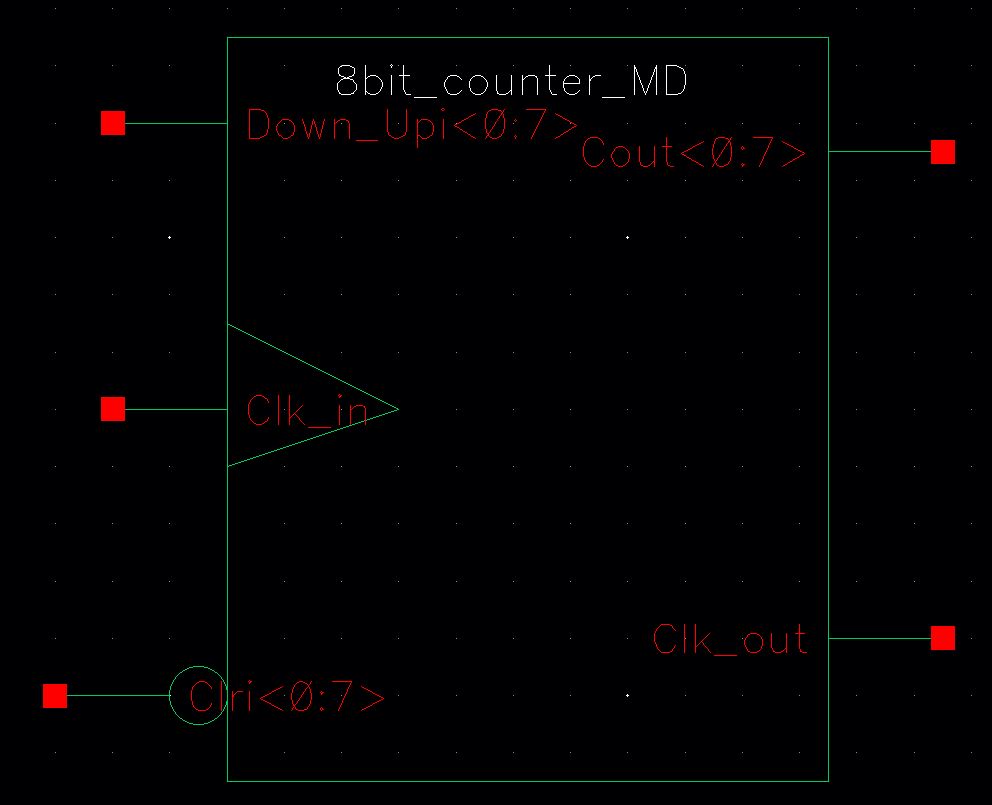
Using 8 of the one bit up/down counter we have and 8 bit counter that will count up 255.
Symbol
Simulations.
Schematic

a. Counting up.
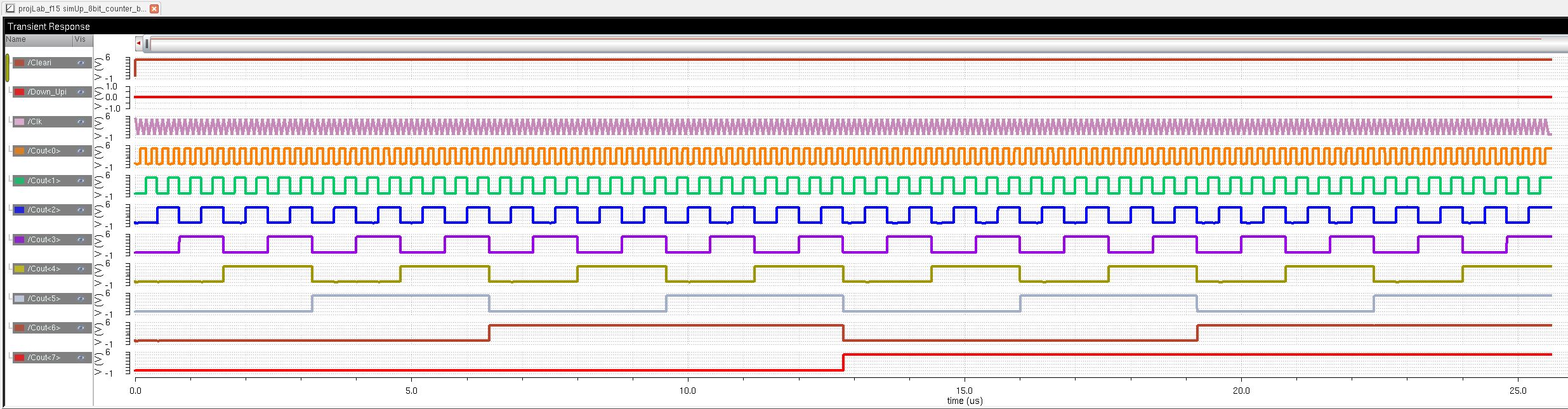
b. Counting down.

c. This simulation shows the counter counting up then reseting and then counts down.

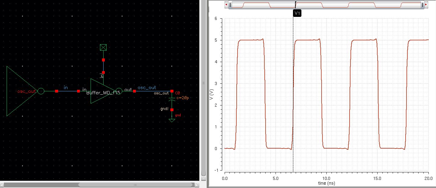
2. A 31-stage ring oscillator with a buffer for driving a 20 pF off-chip load.
31-stage ring oscillator schematic and symbol.
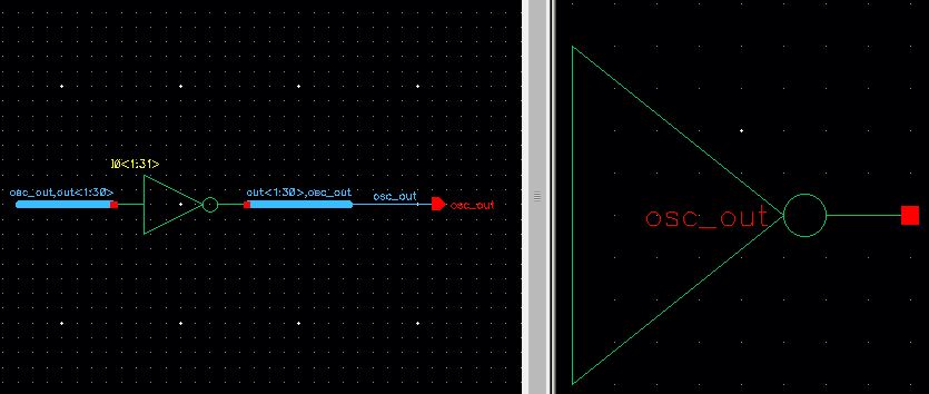
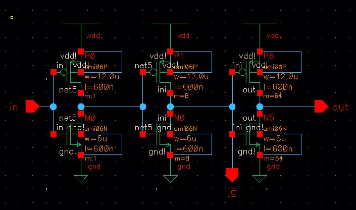
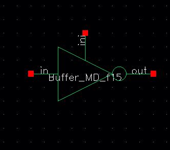
Buffer. The following formula was use to design the buffer, N = ln (Cload/Cin), where N is the number of stages, Cload is the load capacitance, and Cin is the input capacitance of one inverter. For my 12u/6u inverter in the C5 process, Cin is 3/2 (18+9)fF= 40.5fF and Cout is 27fF. N = ln (20pF/40.5fF)= 6.20 or 6 stages. Using 8 for A the number of stages can be reduce to 3.
The ring oscillator with the buffer driving a 20 pF capacitor. Notice that the rise and fall edges are very sharp. Without the buffer, the oscillator won't be avaible to drive this big capacitor.
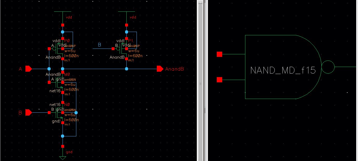
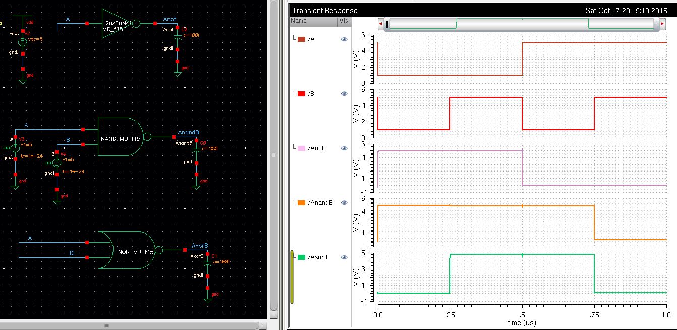
3. NAND and NOR gates using 6/0.6 NMOSs and PMOSs. An inverter made with a 6/0.6 NMOS and a 12/0.6 PMOS.
NAND gate schematic and symbol.
NOR gate schematic and symbol.

Inverter schemactic and symbol.
Simulations of all gates.
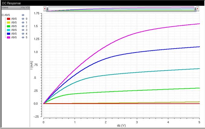
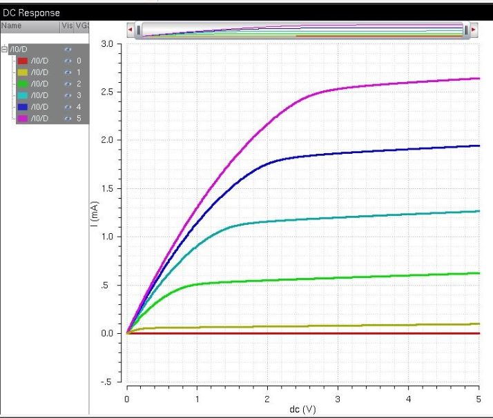
4. Transistors, both PMOS and NMOS, measuring 6u/0.6u where all 4 terminals of each device are connected to bond pads (7 pads + common gnd pad).
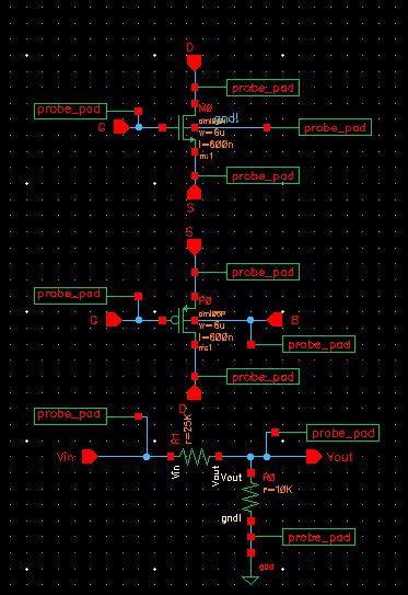
PMOS simulation.
NMOS simulation.
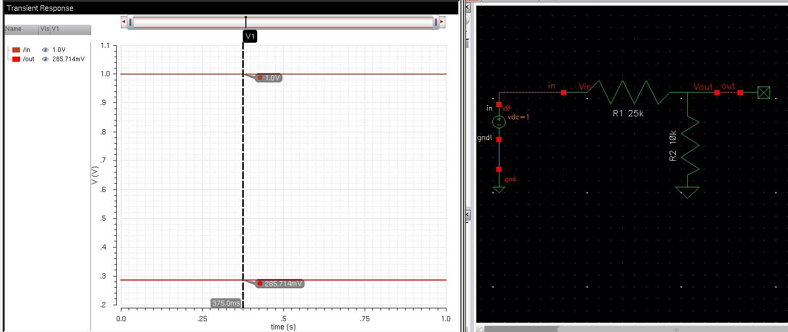
5. Using the 25k resistor laid out below and a 10k resistor implement a voltage divider (need only 1 more pad above the ones used for the 25k resistor) . To calculate Vout, we use Vout/Vin=R1/R1+R2, Vout= 285mV.
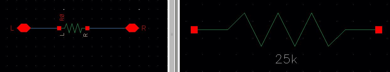
6. A 25k resistor implemented using the n-well (connect between 2 pads but we also need a common gnd pad) . Note that only one pad is need for the common gnd pad. This pad is used to ground the p-substrate and provide ground to each test circuit.
Post-Lab
Layout implementation
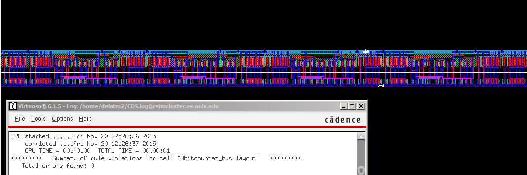
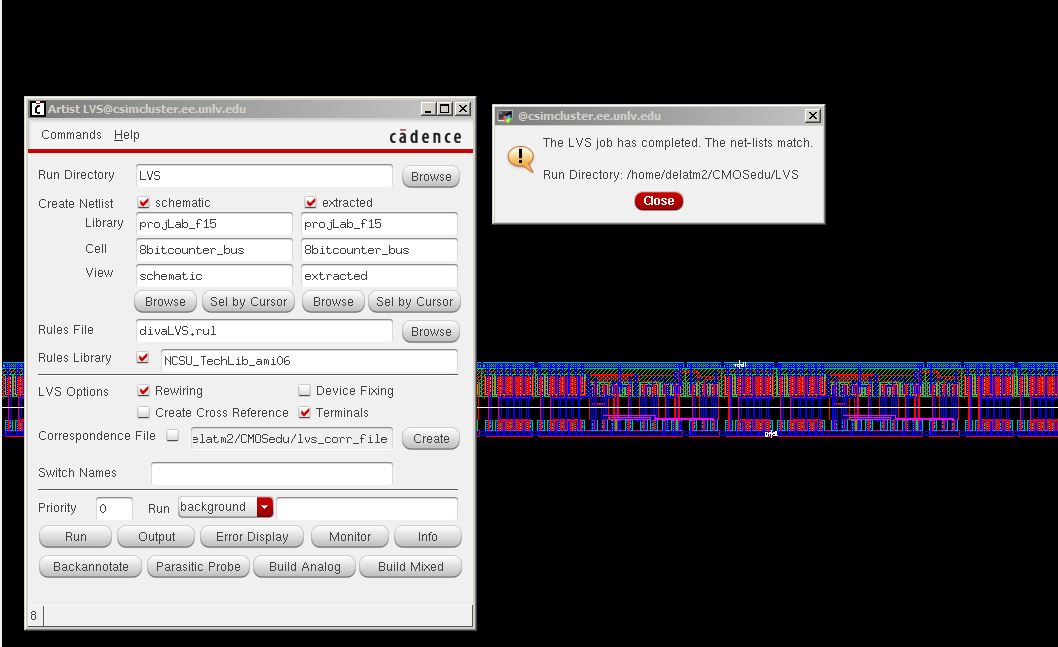
1. 8bit up/down counter layout.
a. DRC
b. LVS
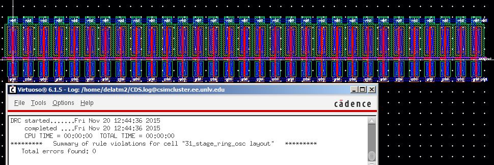
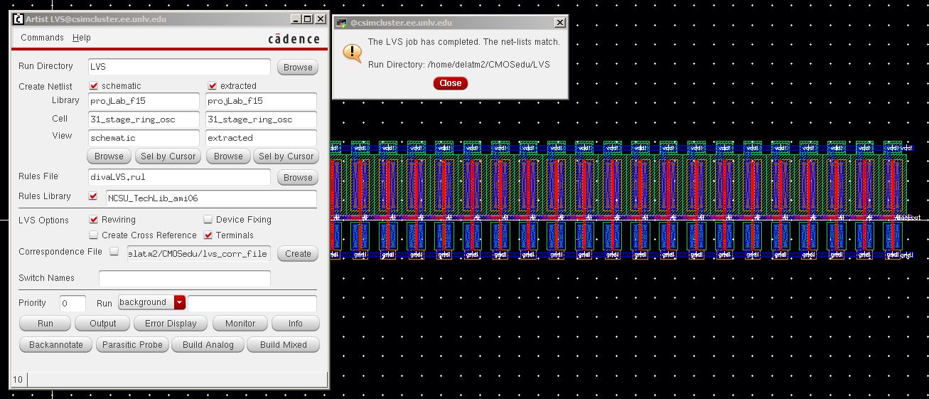
2. A 31-stage ring oscillator layout.
a. DRC
b. LVS
3. A 3 stage buffer layout.
a. DRC
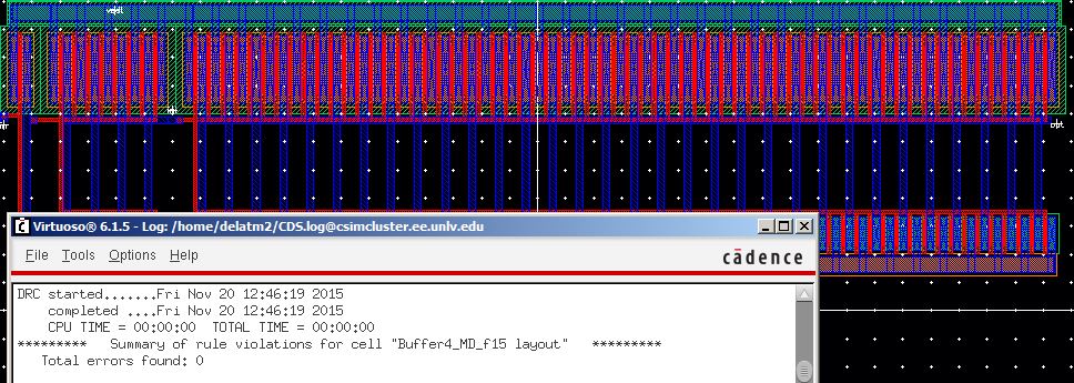
b. LVS

4. NAND and NOR gates using 6/0.6 NMOSs and PMOSs layout.
a. DRC
| NAND | NOR |
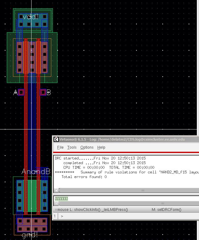 | 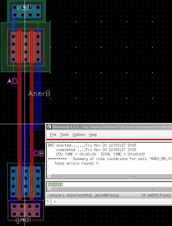 |
b. LVS
| NAND | NOR |
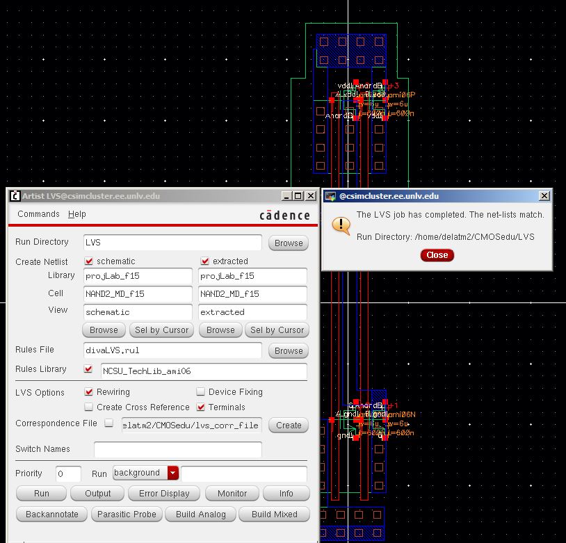 | 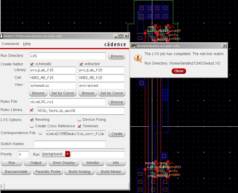 |
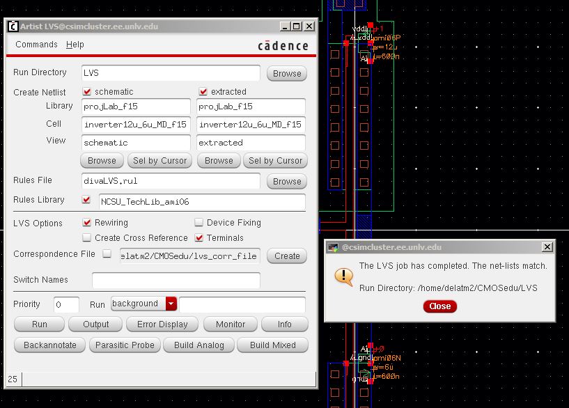
5. An inverter made with a 6/0.6 NMOS and a 12/0.6 PMOS layout.
LVS
6. Transistors, both PMOS and NMOS, measuring 6u/0.6u layout.
LVS
NMOS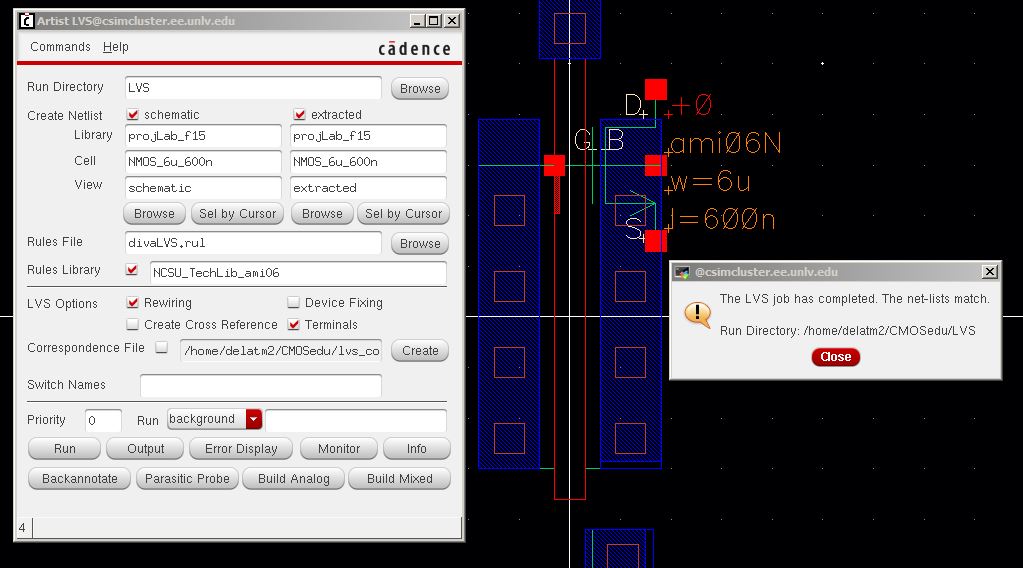

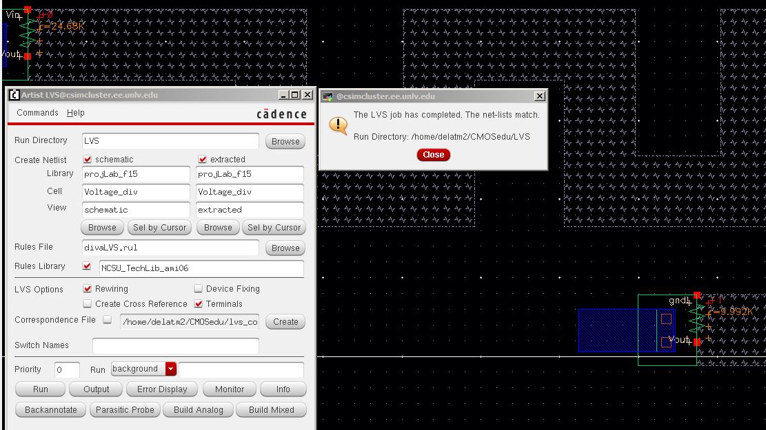
7. Voltage divider 25k and 10k layout.
LVS
Backing up my work.
1. A zip folder will be created Lab2.
2. Then the zipped folder will be store on my google drive.