Lab 7 - EE 421L Fall 2015
Zip folder containing Lab7 files found here
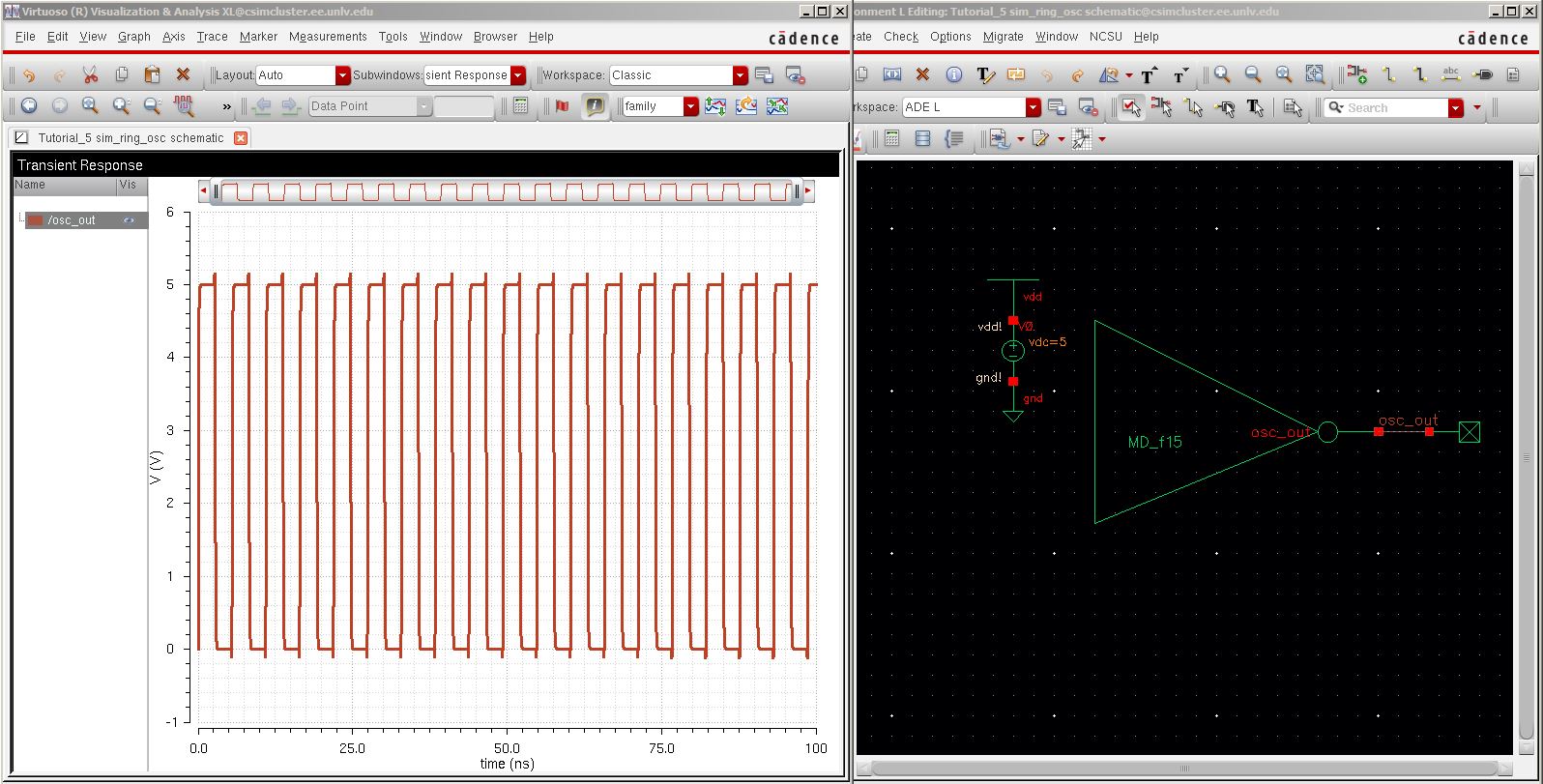
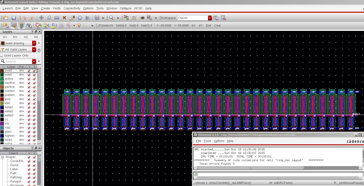
Tutorial 5 is about design, layout and simulation of the a ring oscillator.
1. The schematic and symbol views for the ring oscillator.
2. Simulation and schematic.
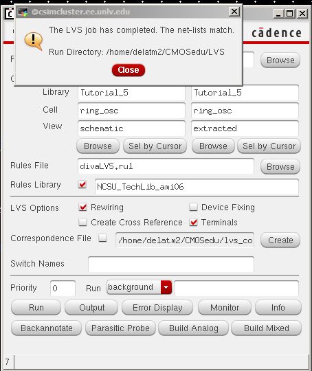
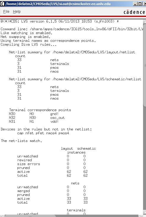
4. LVS with no errors.
This concludes this tutorial.
Post-Lab
1. Creating a 4 bit inverter using a bus line.
a. Schematic and symbol.

b. Simulation of the 4bit inverter. Notice than the capacitive loads affect the rise and fall time delays of the inverters. With no load capacitor (out<0>) or small capacitance (out<3>) the output is the same as the input, no rise/fall time delay. The larger the capacitve load the longer the rise/fall time delays (out<1>).

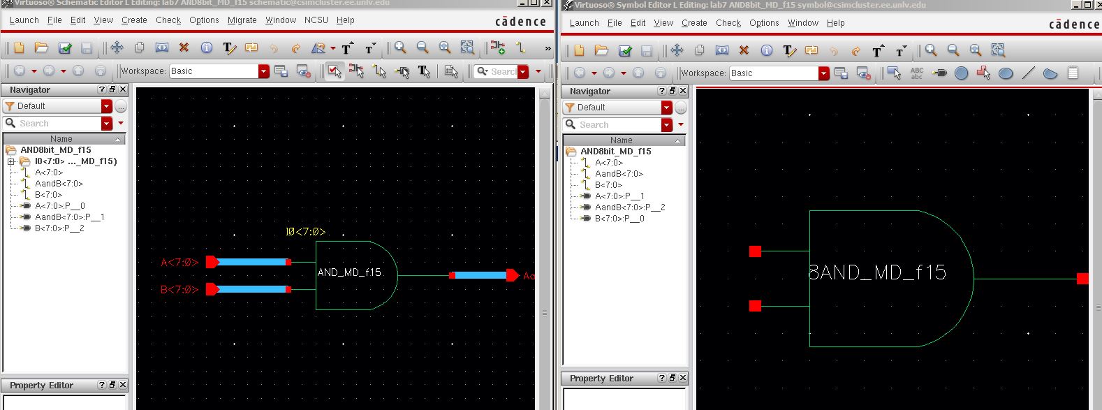
2. Creating an 8 bit and gate using a bus line.
a. Schematic and symbol.
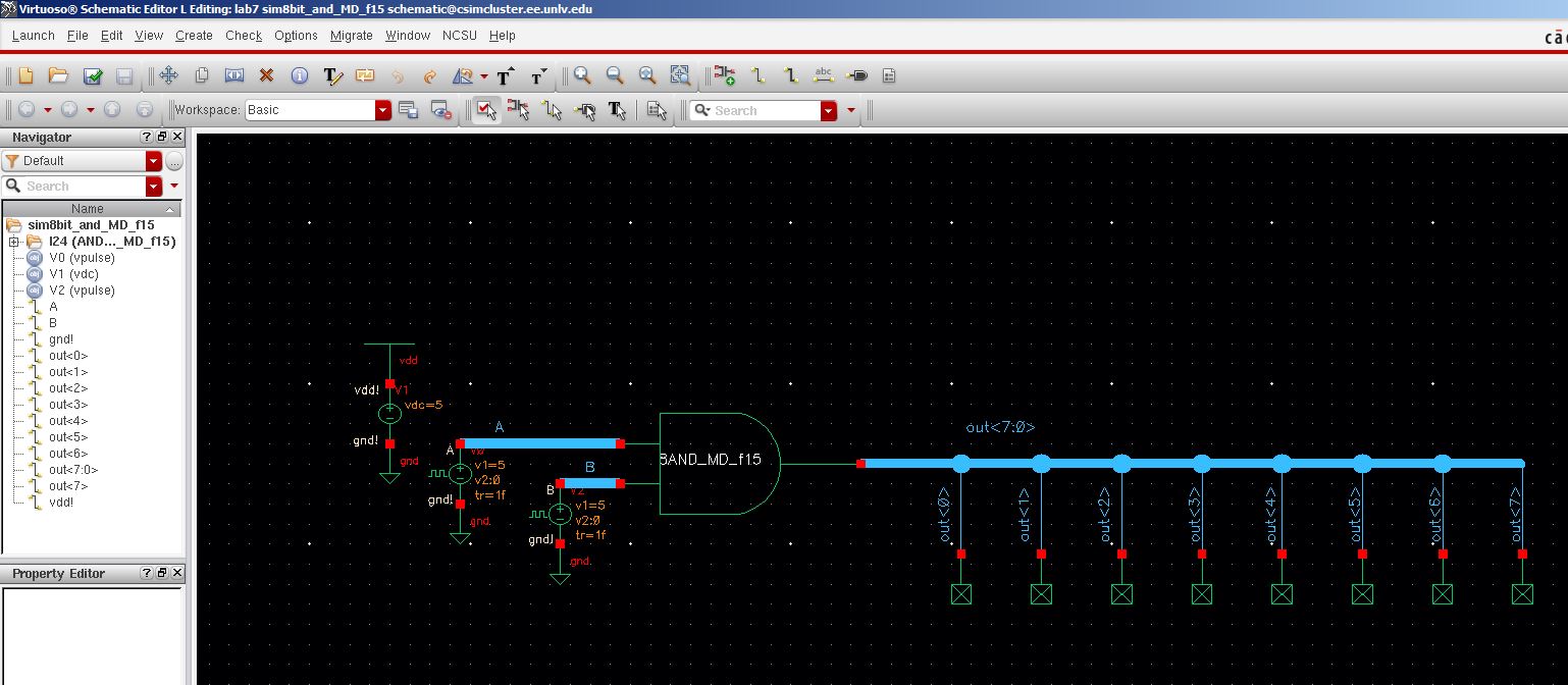
b. Simulation of the 8 bit and gate.

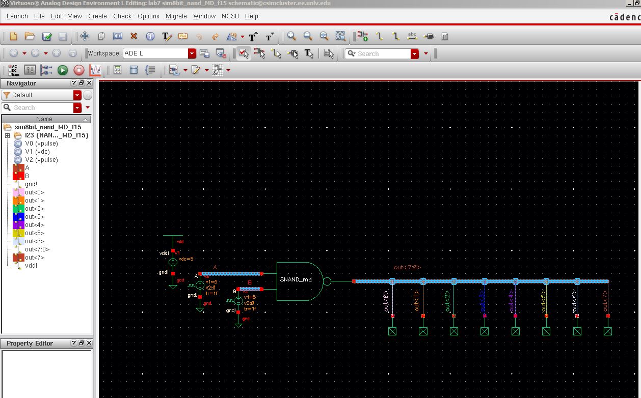
3. Creating an 8 bit nand gate using a bus line.
a. Schematic and symbol.
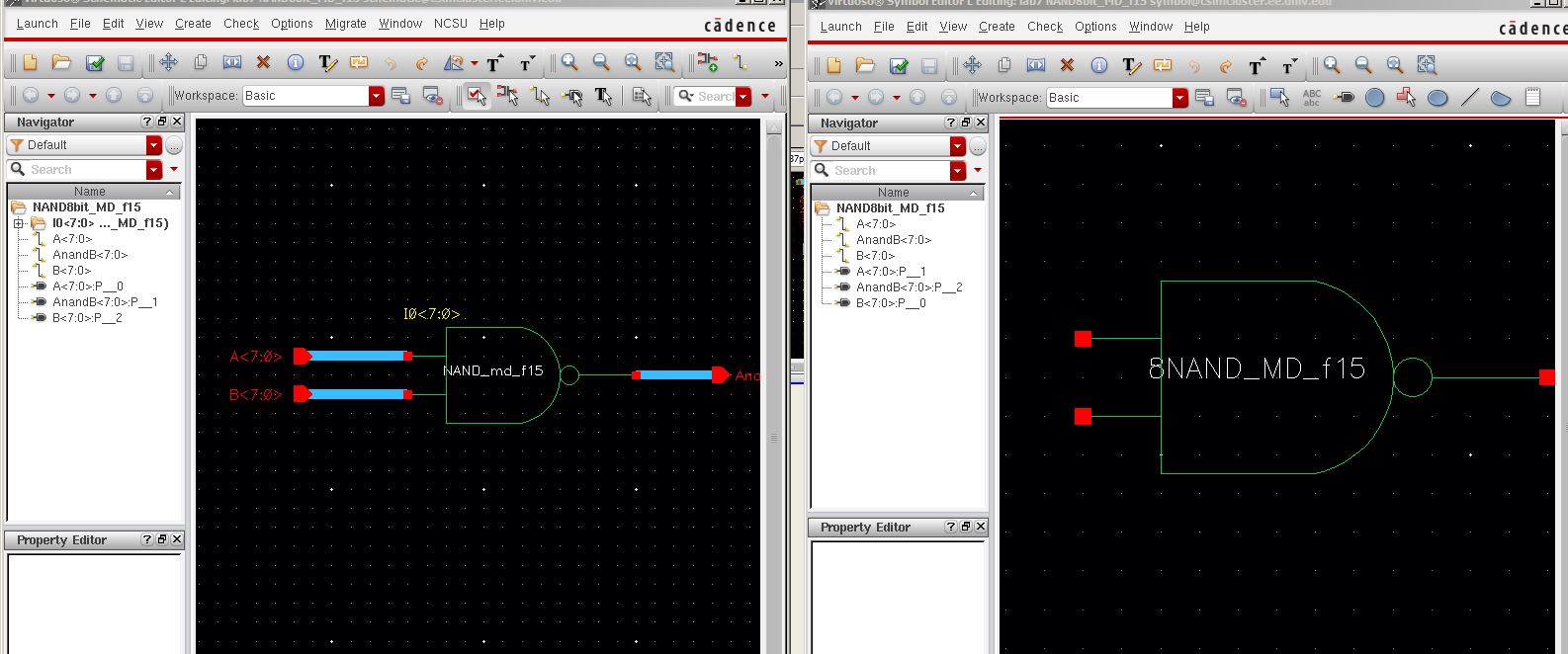
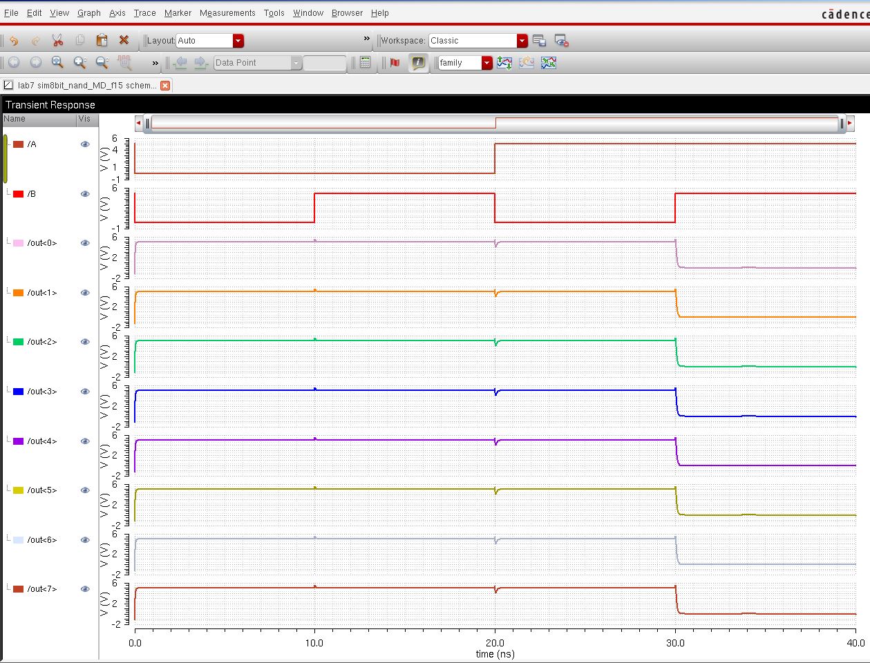
b. Simulation of the 8 bit nand gate.
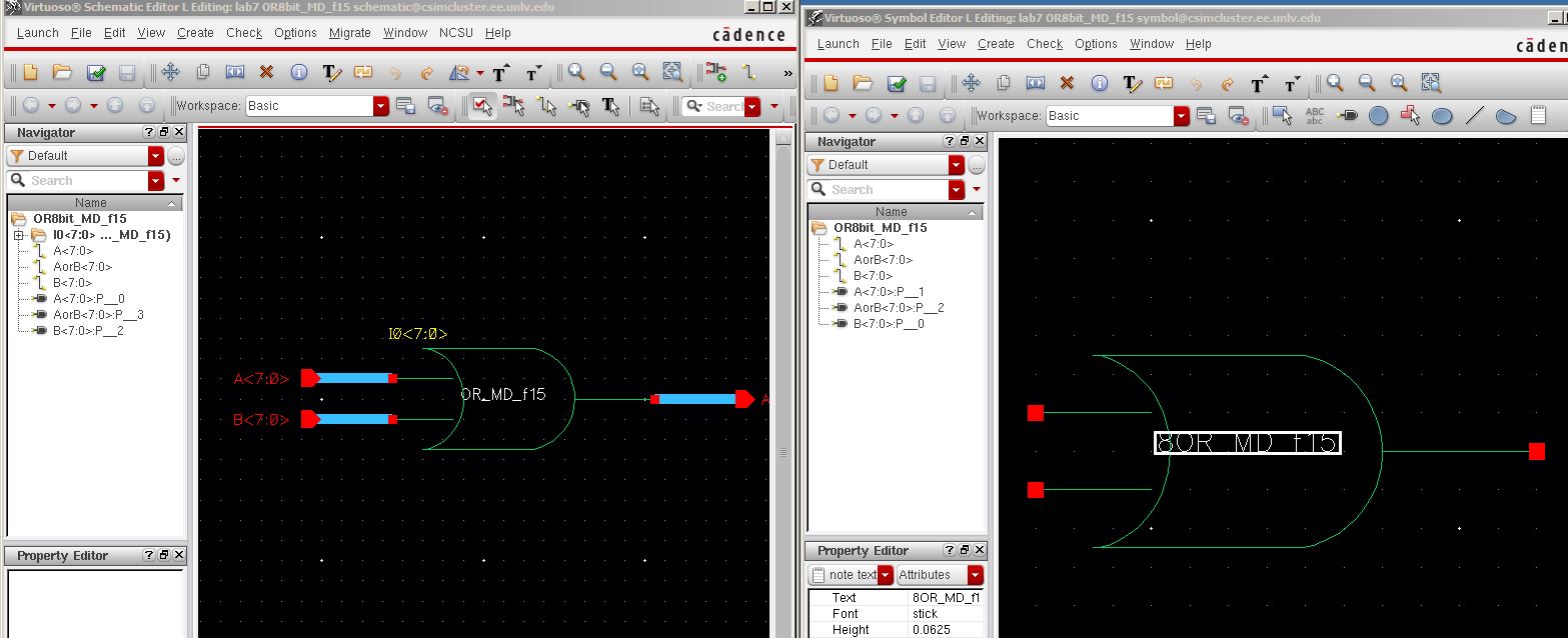
4. Creating an 8 bit or gate using a bus line.
a. Schematic and symbol.
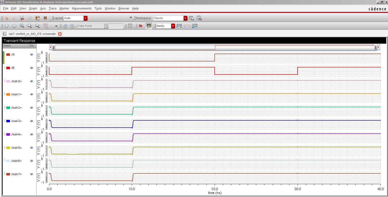
b. Simulation of the 8 bit or gate.

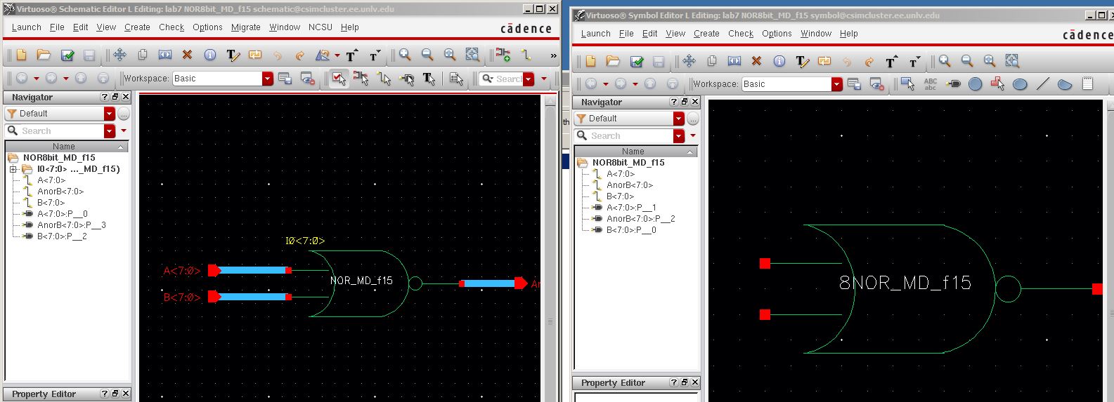
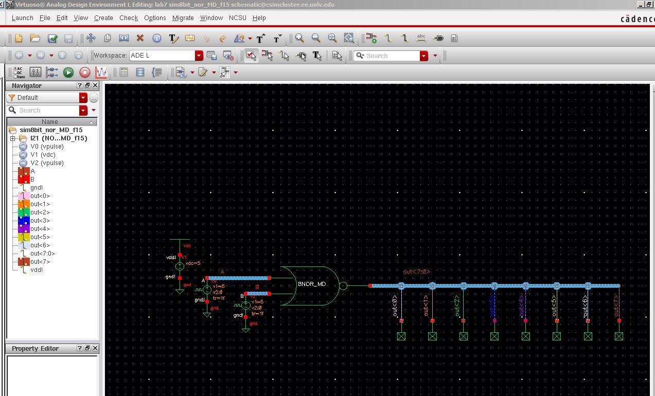
5. Creating an 8 bit nor gate using a bus line.
a. Schematic and symbol.
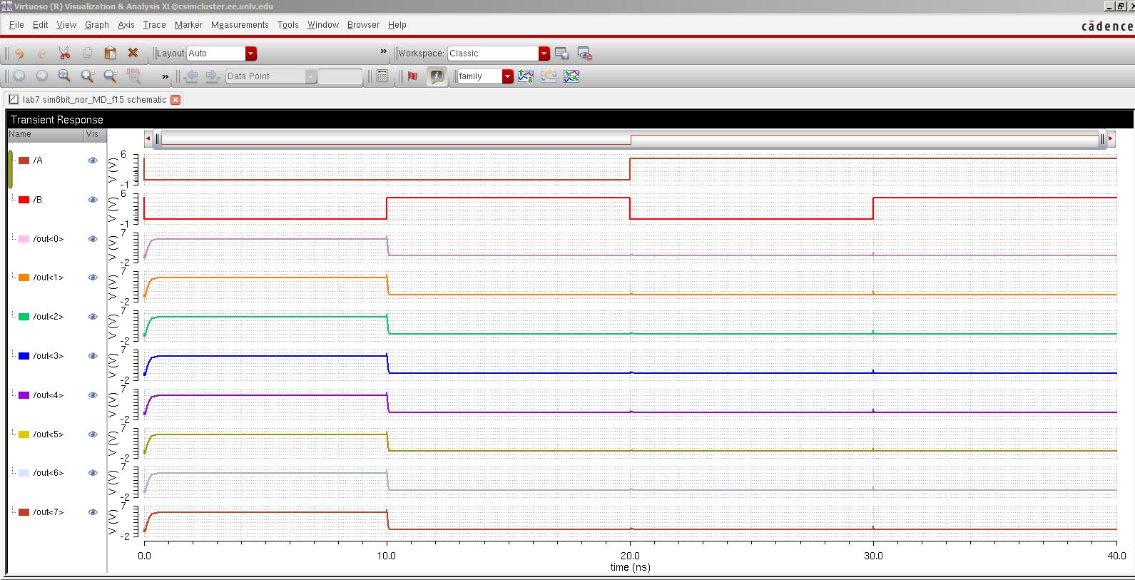
b. Simulation of the 8 bit nor gate.
6. Creating an 8 bit inverter using a bus line.
a. Schematic and symbol.

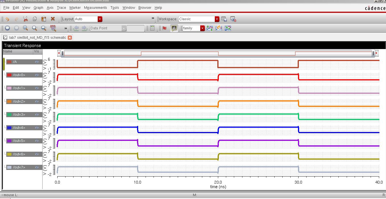
b. Simulation of the 8 bit inverter.

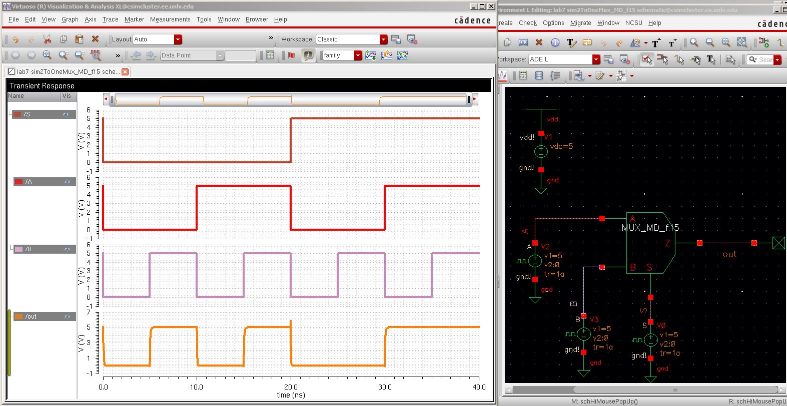
7. Creating a 2 to 1 mux.
a. Schematic and symbol mux. The mux circuit consists of 3 inputs and 1 outputs. One input is S, when it's high input A is going to pass through output Z. When S is low input B is going to pass through. The mux chooses between A and B depending on S.

b. Simulation of the 2 to 1 mux.
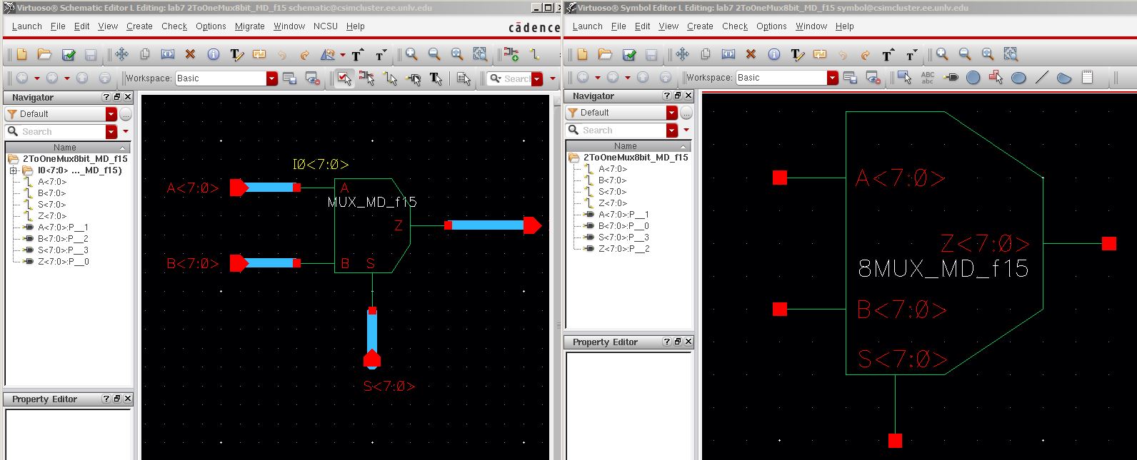
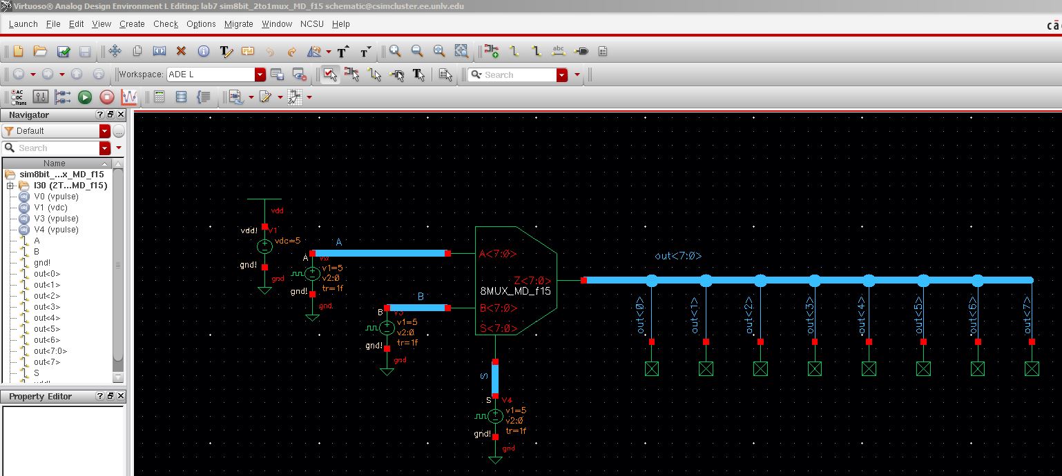
An 8 bit mux.
a. Schematic and symbol.
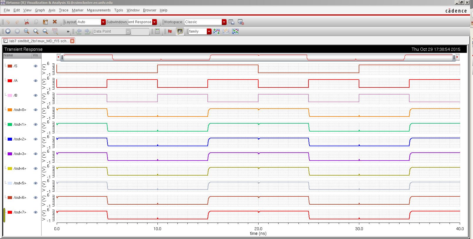
b. Simulation of the 8 bit 2 to 1 mux.
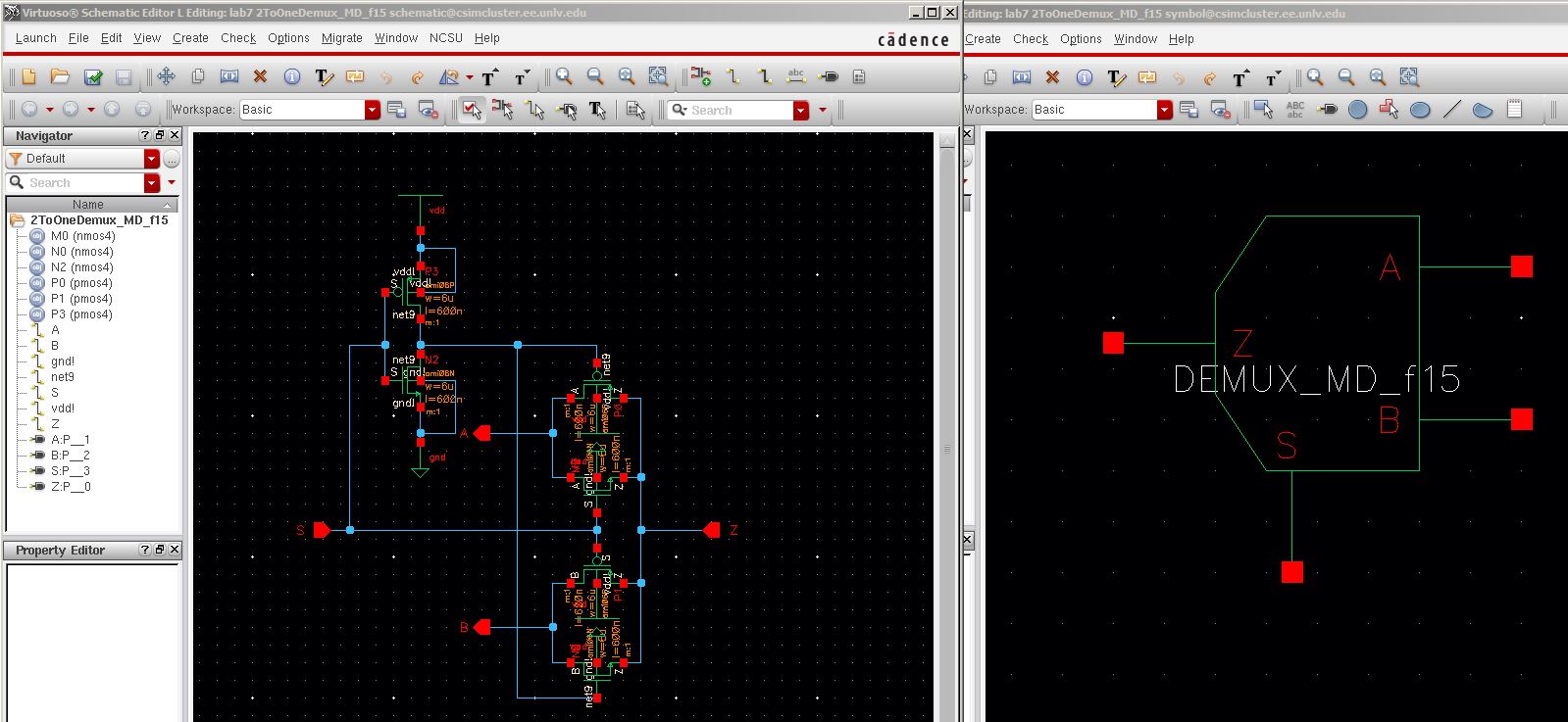
8. Creating a 2 to 1 demux.
a. Schematic and symbol. A demux is going to route the input Z to output A or B depending on the input S.
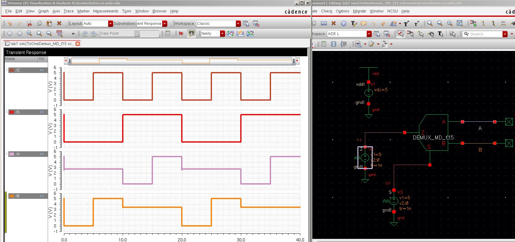
b. Simulation of the 2 to 1 demux.
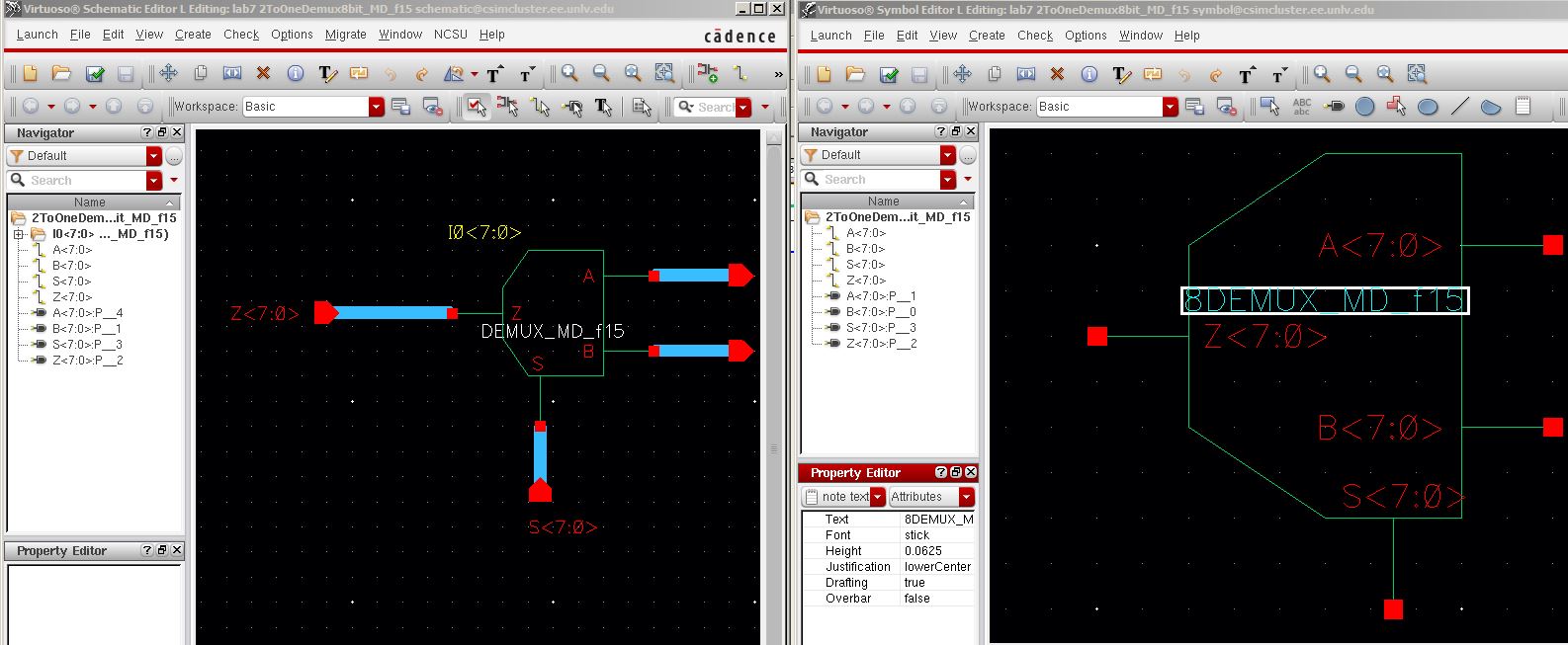
An 8 bit demux.
a. Schematic and symbol.
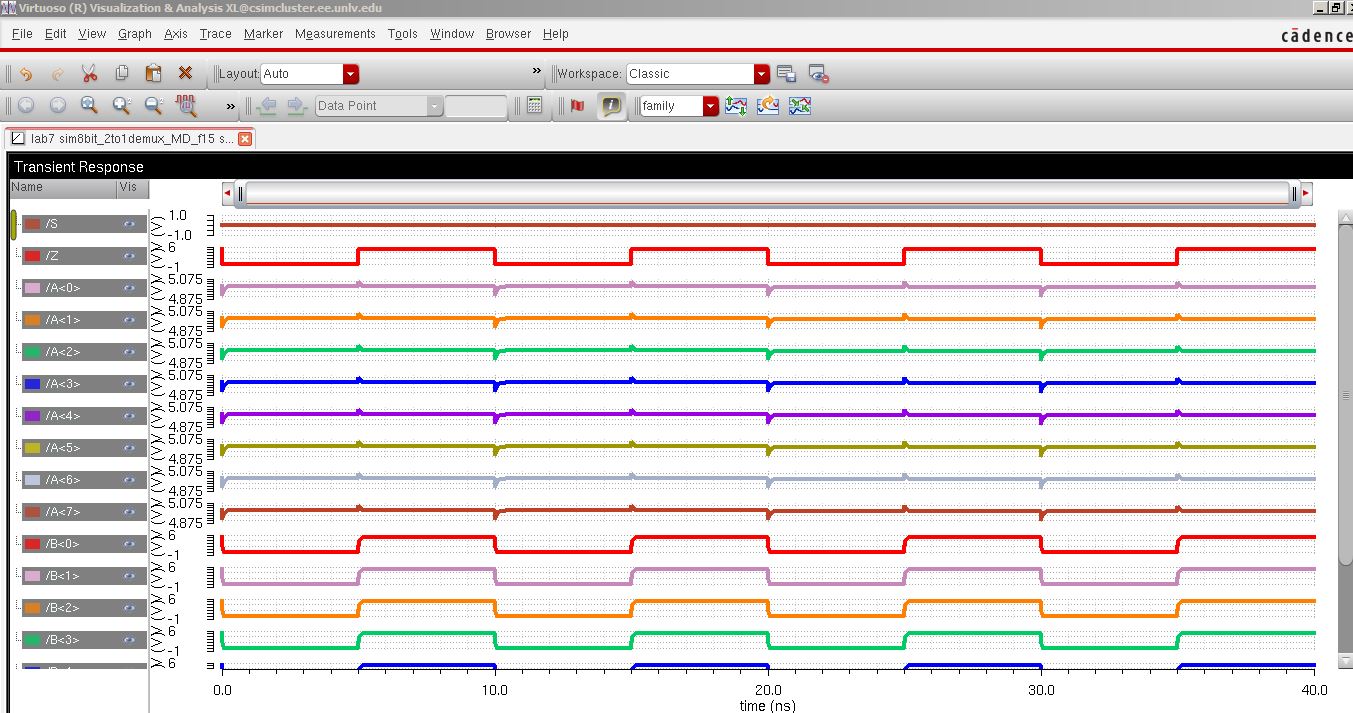
b. Simulation.

A output.
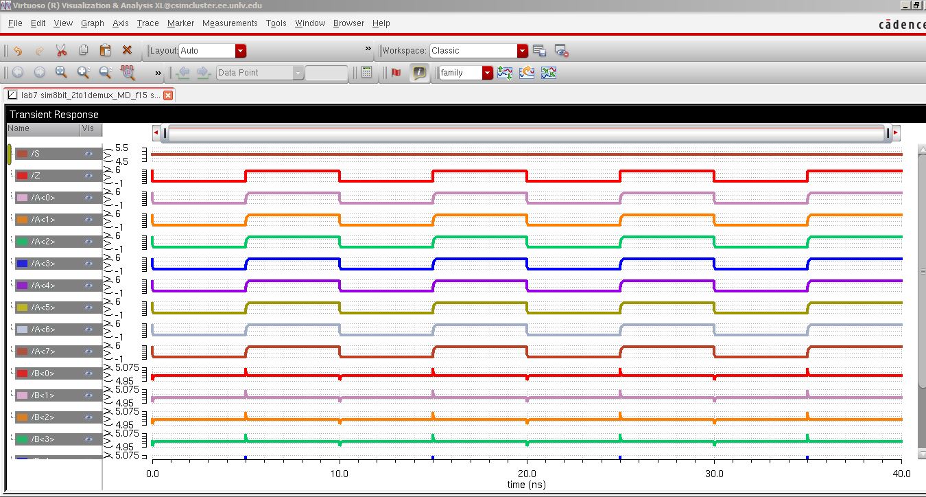
B output.
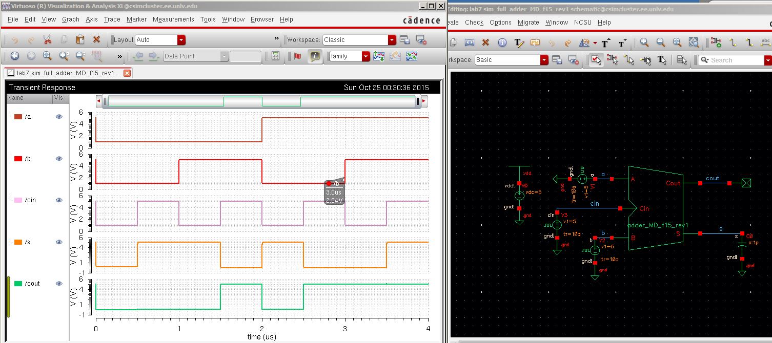
9. Creating a full adder.
a. Schematic (From fig12.20) and symbol.
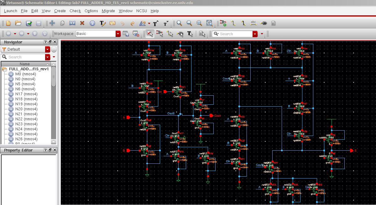
Layout and DRC.
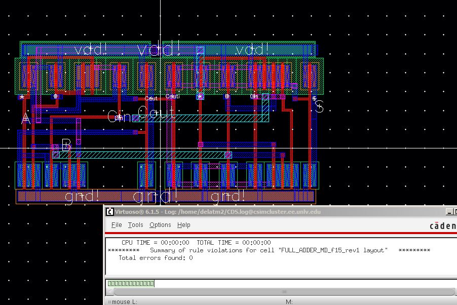
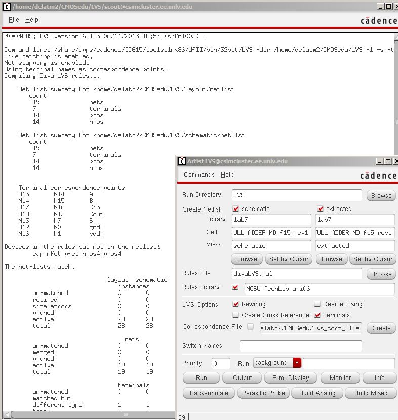
LVS.
b. Simulation of the full adder.
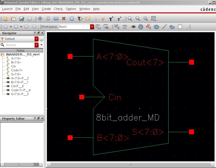
An 8 bit full adder.
a. Schematic and symbol.

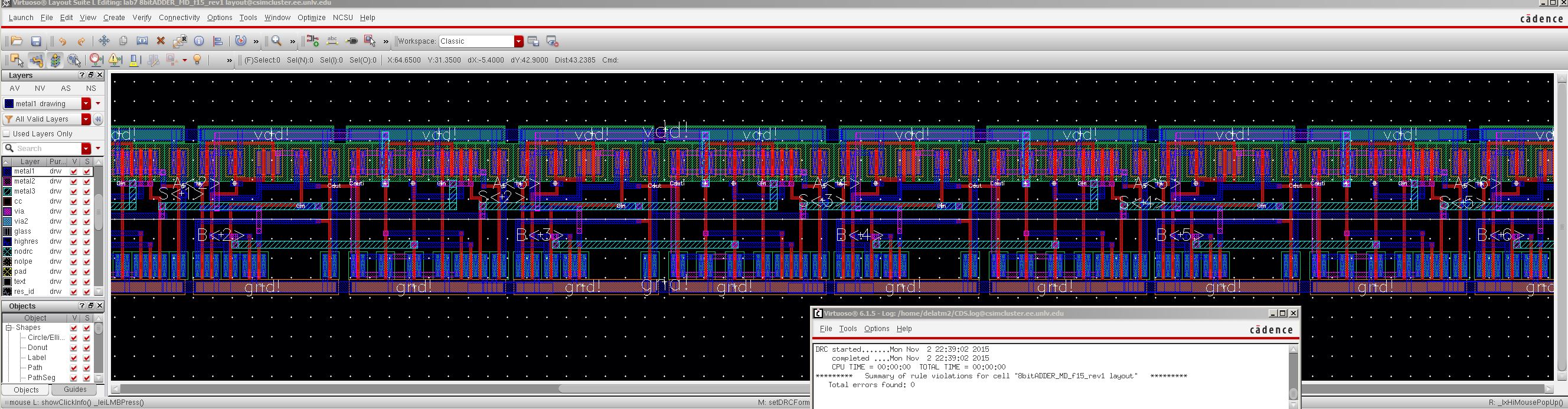
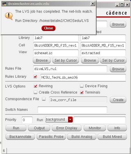
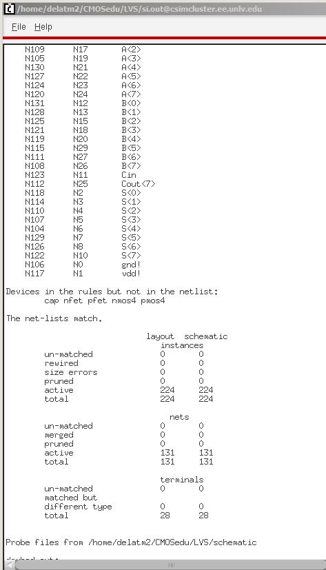
b. DRC and LVS.
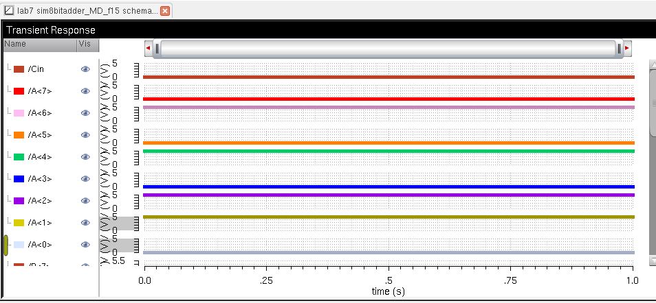
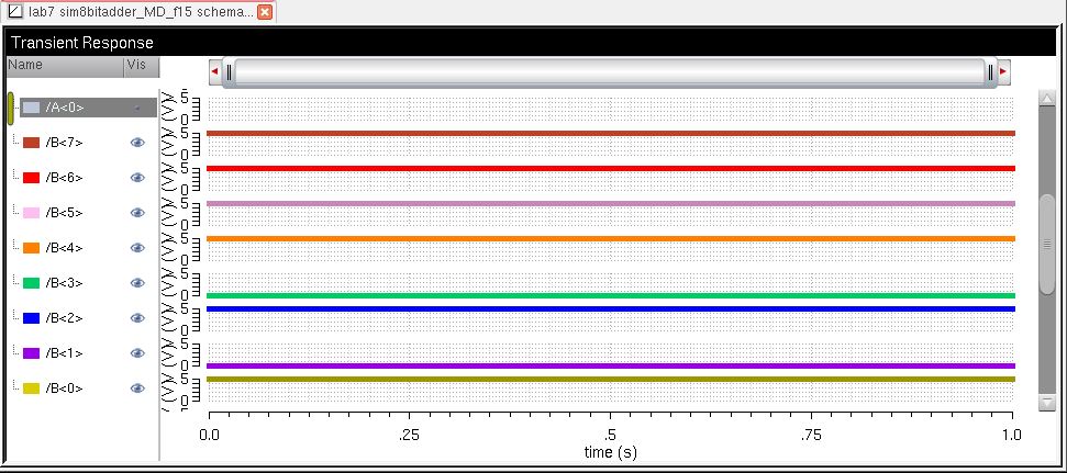
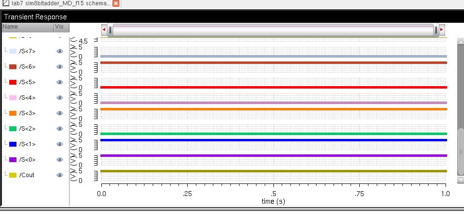
c. Simulation of the 8 bit full adder.

A input = 01010110, Cin= 0
B input= 11110101
S<7:0>= 01001011 and Cout = 1 so A+B= 101001011
Backing up my work.
1. A zip folder will be created Lab2.
2. Then the zipped folder will be store on my google drive.