Lab 6 - EE 421L Fall 2015
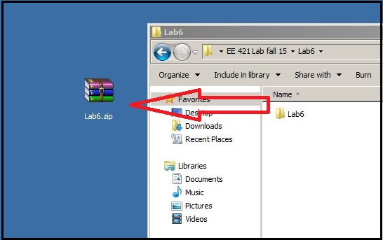
Zip folder containing Lab6 files found here.
This tutorial is about the design, layout, and operation of a NAND gate.
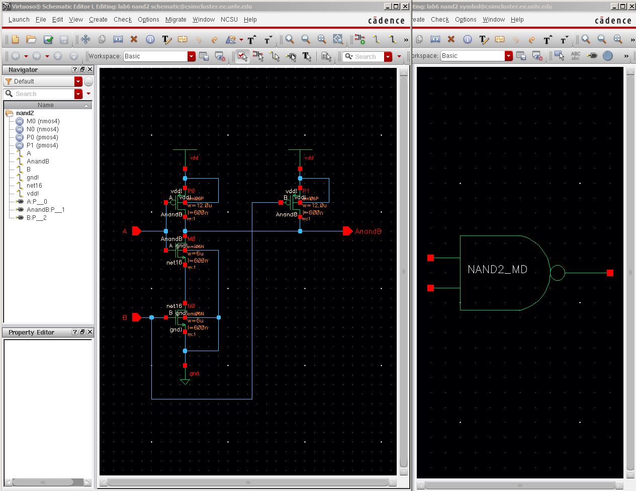
1. The schematic of the NAND gate using NMOS and PMOS of 6um/.6um.
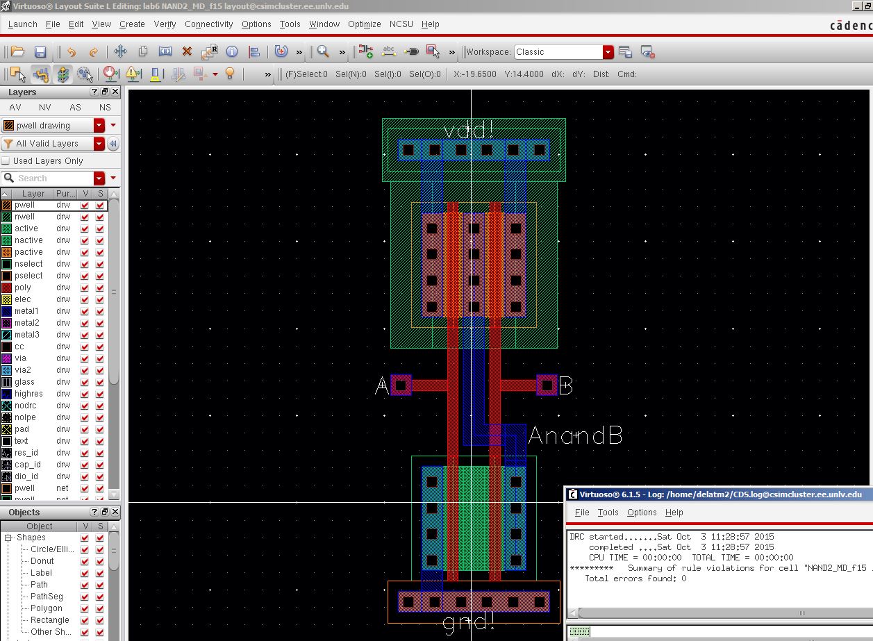
2. Layout and DRC.
3. Extracted view.

4. LVS with no errors.
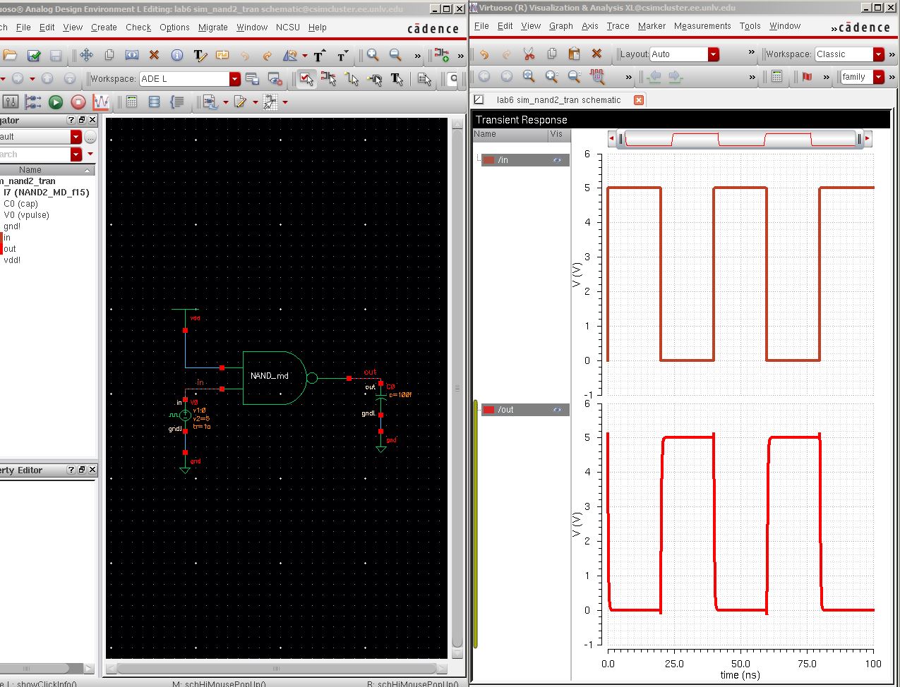
5. Simulation and schematic.
This concludes this tutorial.
Post-Lab
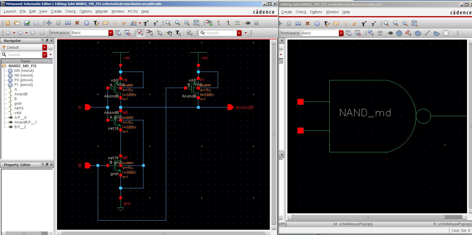
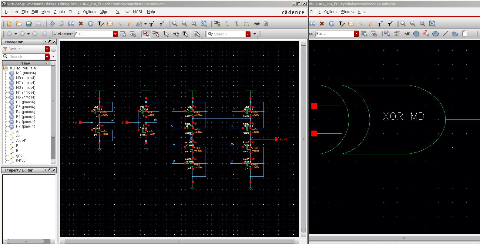
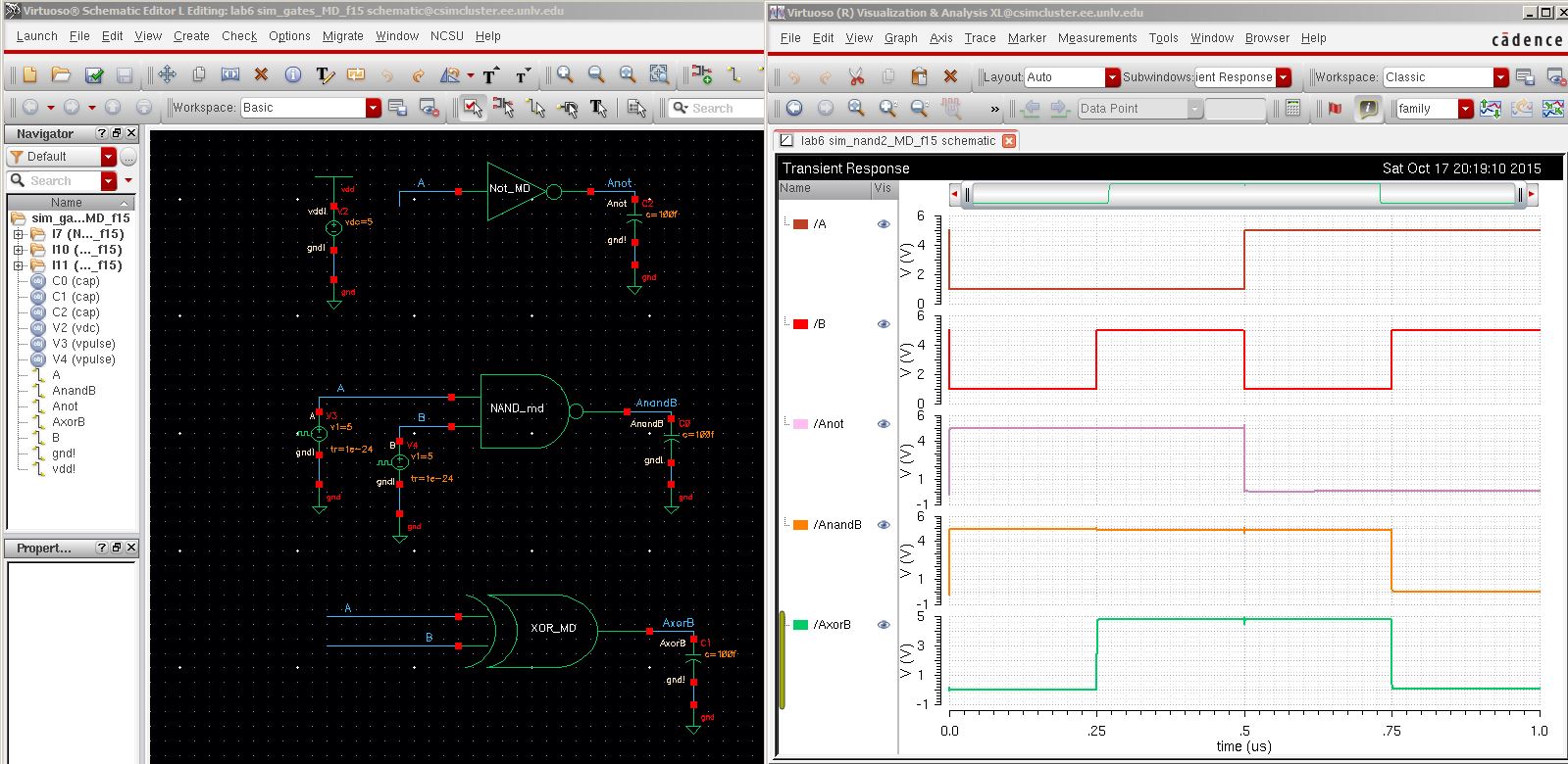
1. Schematic and symbol views for 2-input NAND and XOR gates.
NAND gate.
XOR gate.
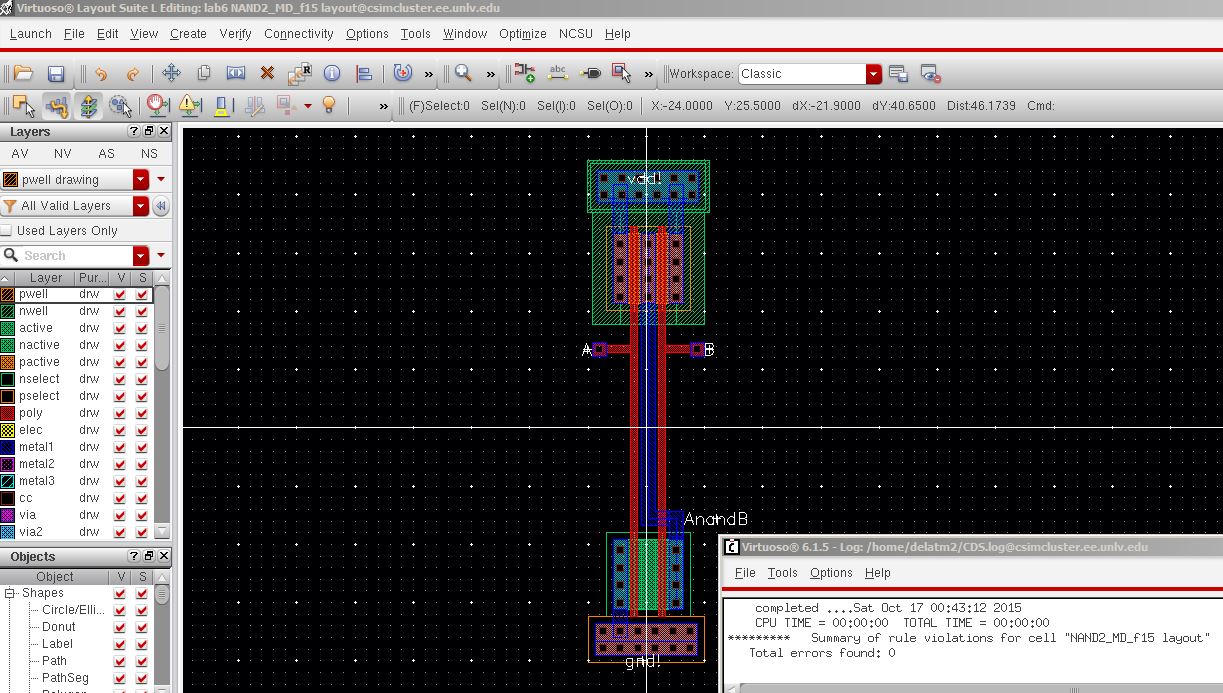
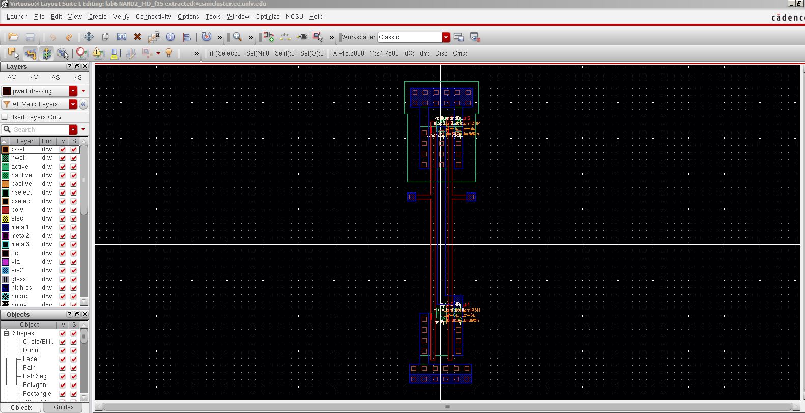
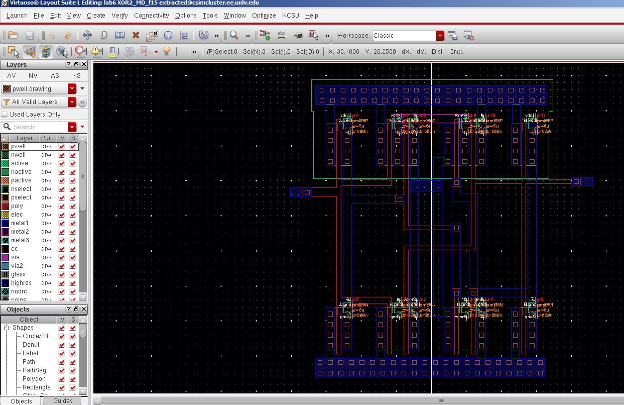
2. Layout and extracted views for 2-input NAND and XOR gates.
NAND gate.
XOR gate.

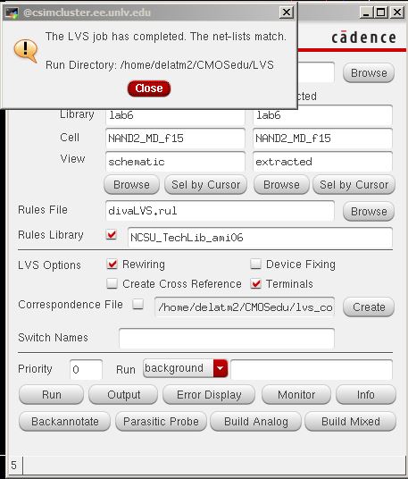
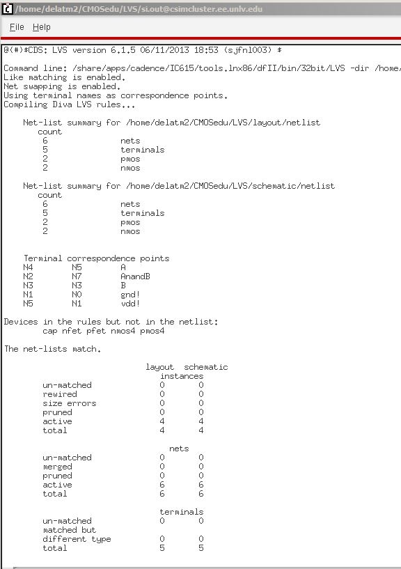
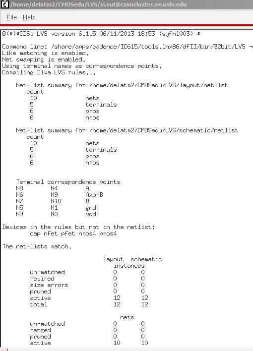
3. LVS.
NAND gate.
XOR gate.
4. Simulations were exactly as expected for the gates, all four possible inputs were tested. There are some glitches on the output of the NAND and XOR gates due to the rise and fall timing of the input signals.
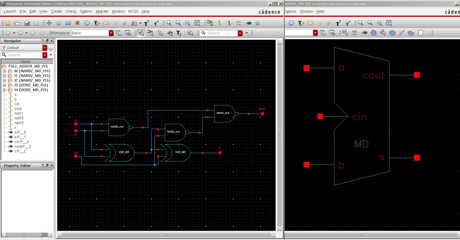
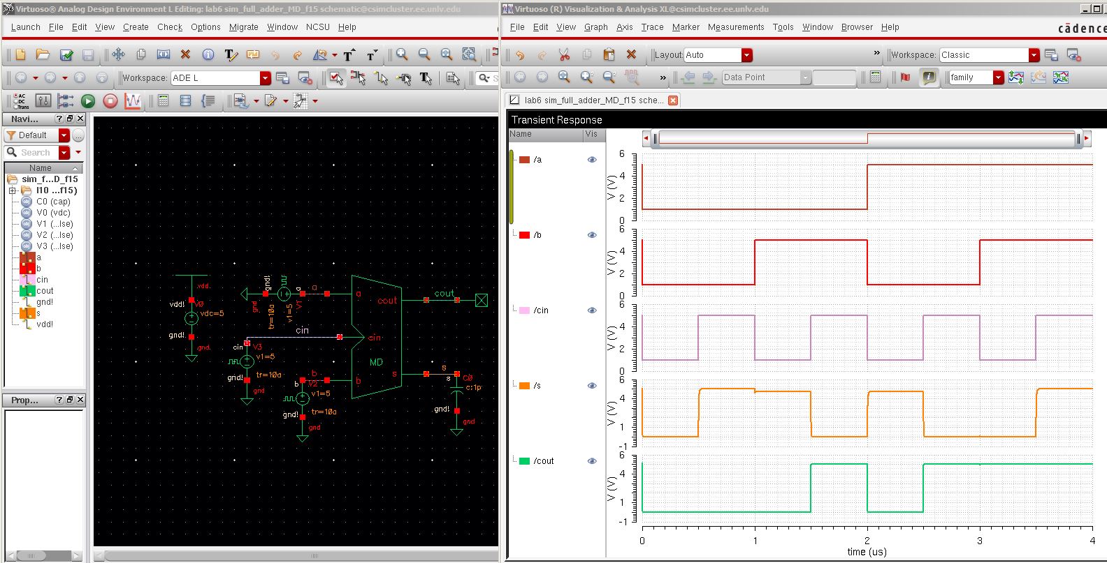
5. Schematic and symbol views for the full adder.
Simulations follow the truth table.
|
a |
b |
cin |
s |
cout |
|
|
0 |
0 |
0 |
0 |
0 |
|
|
0 |
0 |
1 |
1 |
0 |
|
|
0 |
1 |
0 |
1 |
0 |
|
|
0 |
1 |
1 |
0 |
1 |
|
|
1 |
0 |
0 |
1 |
0 |
|
|
1 |
0 |
1 |
0 |
1 |
|
|
1 |
1 |
0 |
0 |
1 |
|
|
1 |
1 |
1 |
1 |
1 |
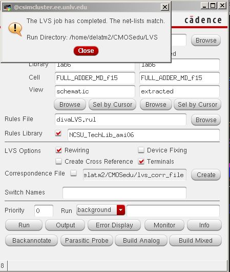
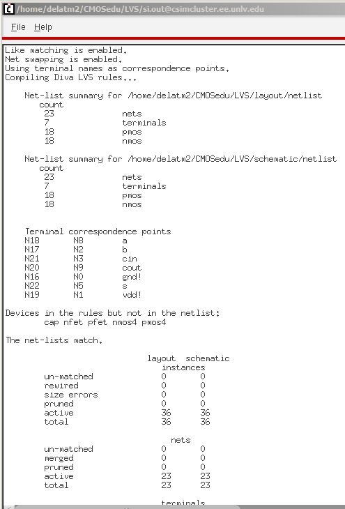
6. Layout and extracted views for the full adder.
Layout and DCR with no errors.

Extracted view.
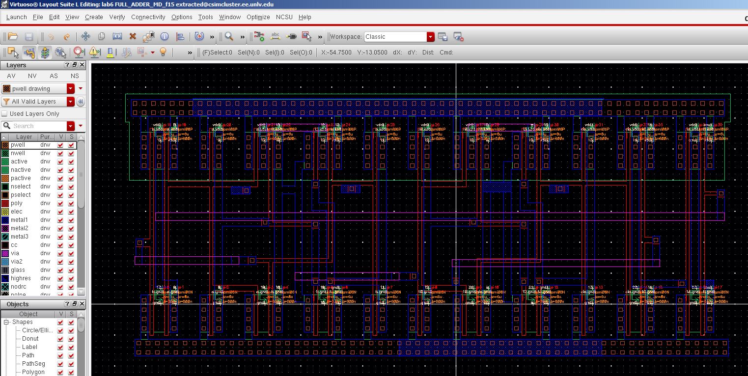
LVS with no errors.
Backing up my work.
1. A zip folder will be created Lab2.
2. Then the zipped folder will be store on my google drive.