Lab 4 - EE 421L Fall 2015
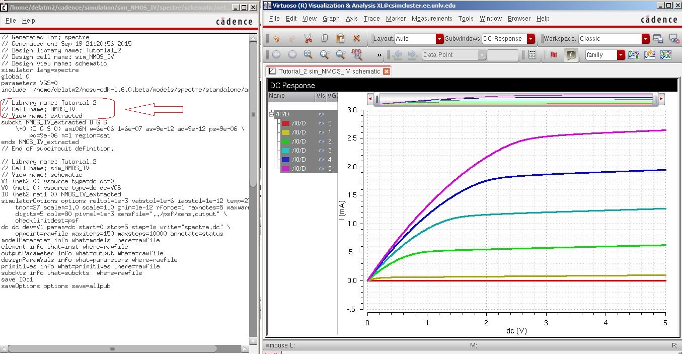
8. Simulation with the extracted
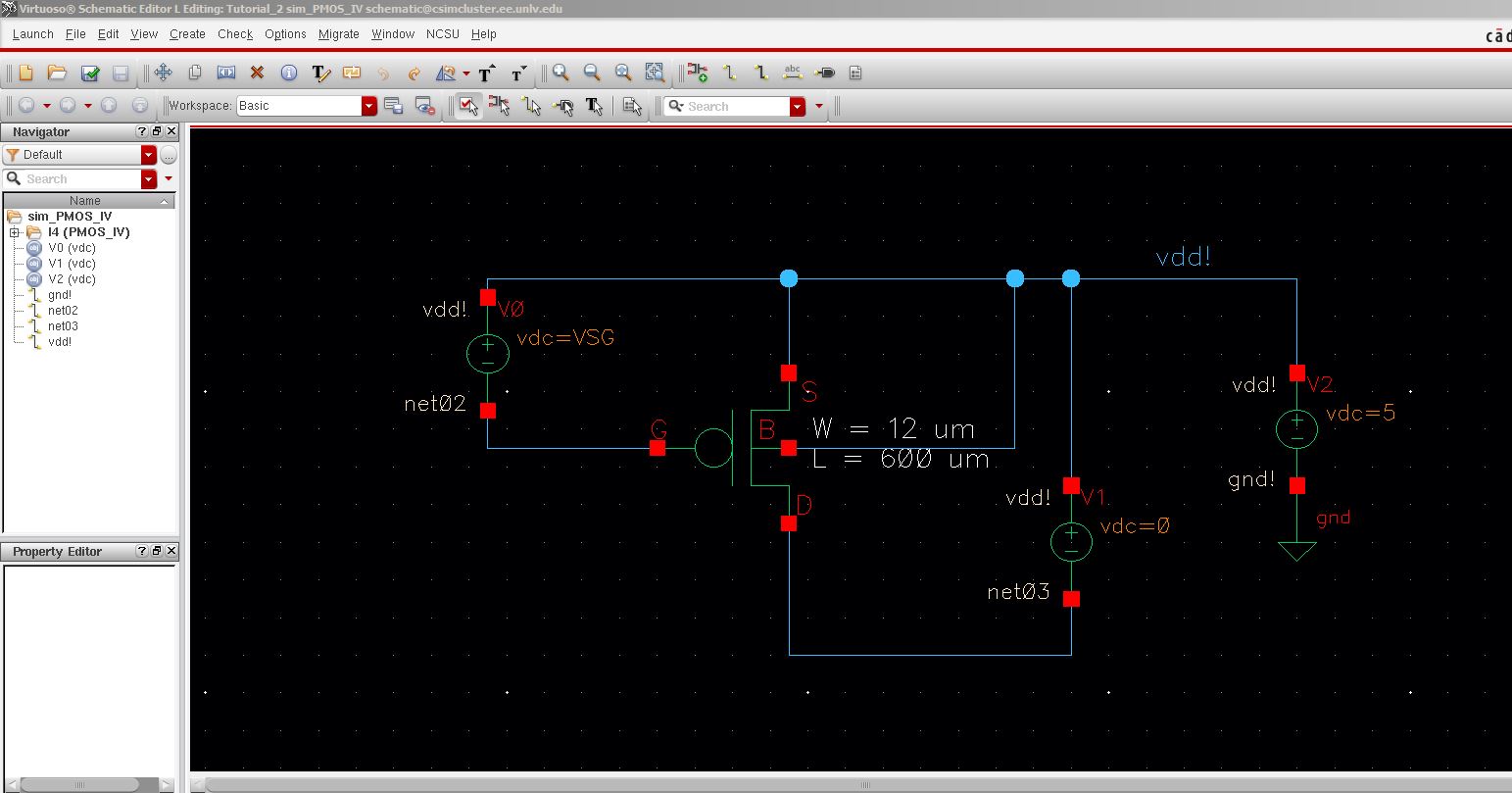
9. A similar procedure was followed for the PMOS.
a. Schematic with pins G, S, D and B. And then a symbol was created.

10. Layout and extracted of the PMOS.

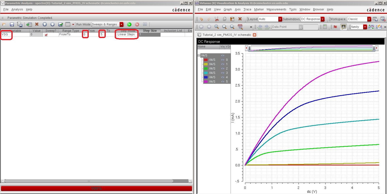
11. Simulation.
12. Open ADE L and run the simulation.
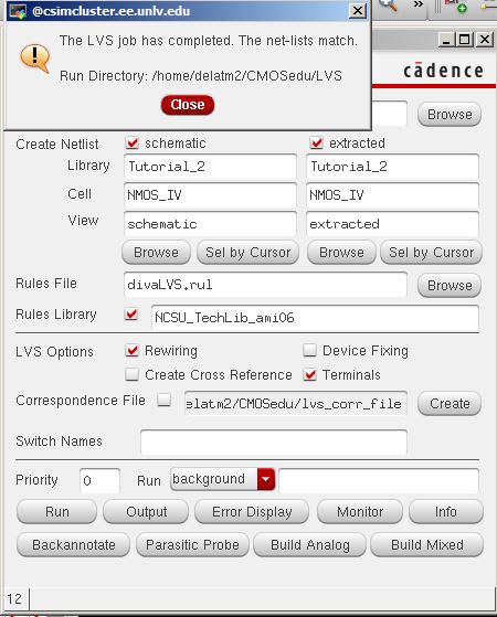
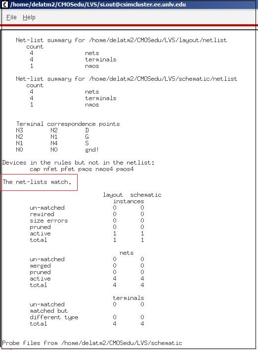
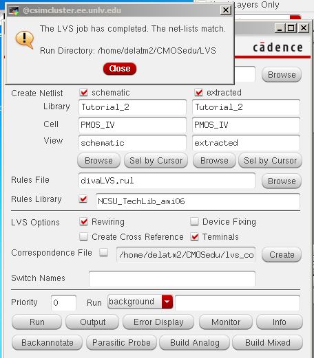
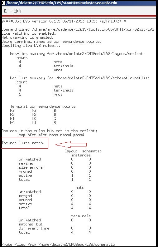
13. LVS with no errors.
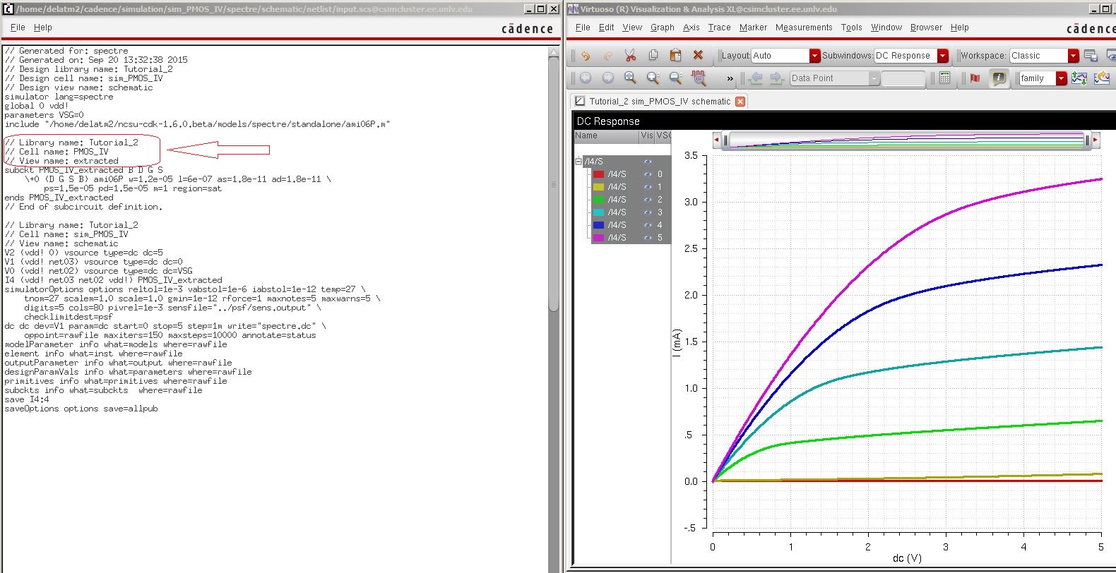
14. And finally the simulation with the extracted.
This concludes tutorial 2.
Post Lab
NMOS Device.
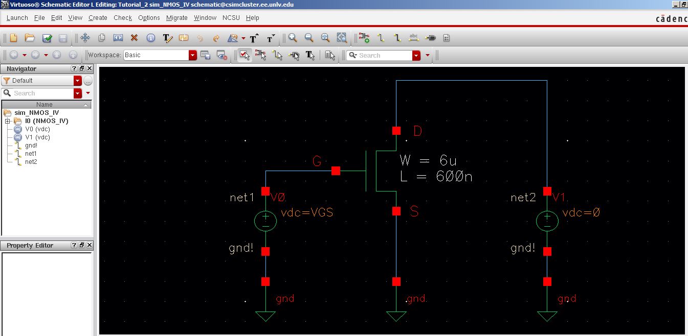
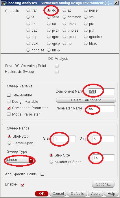
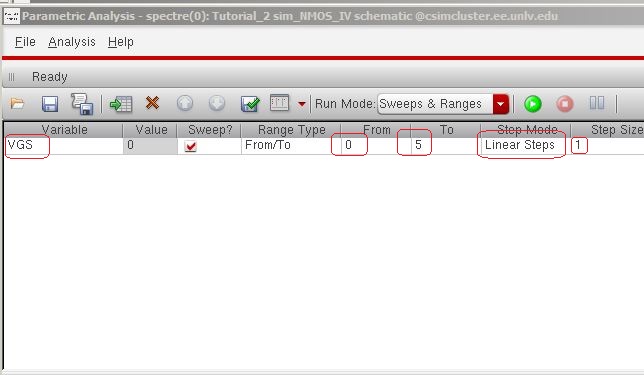
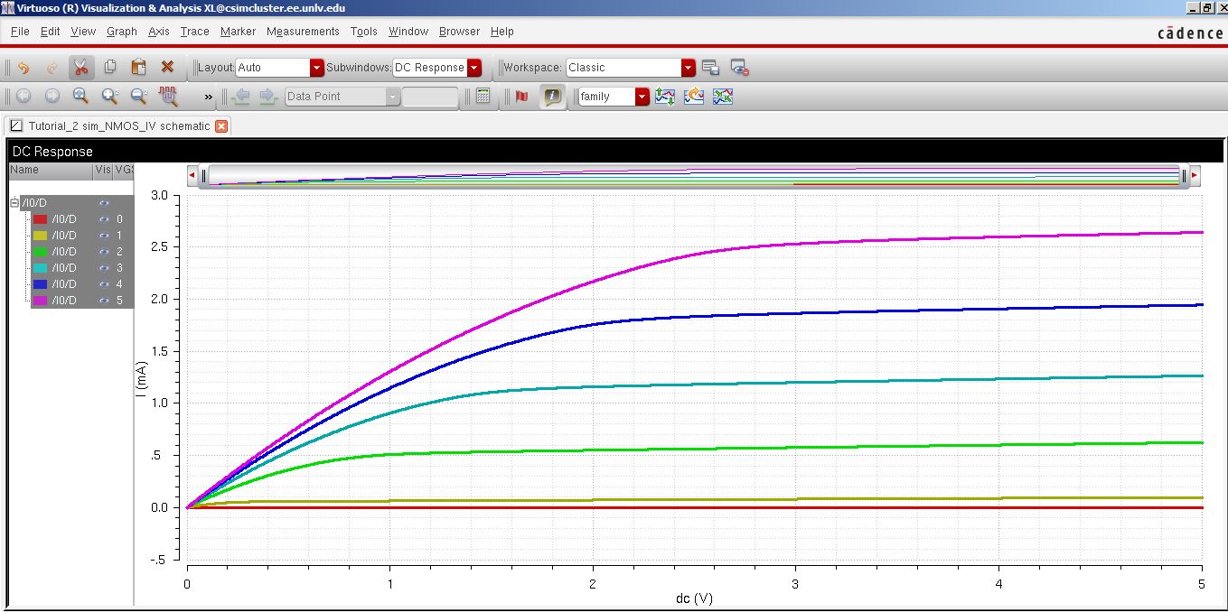
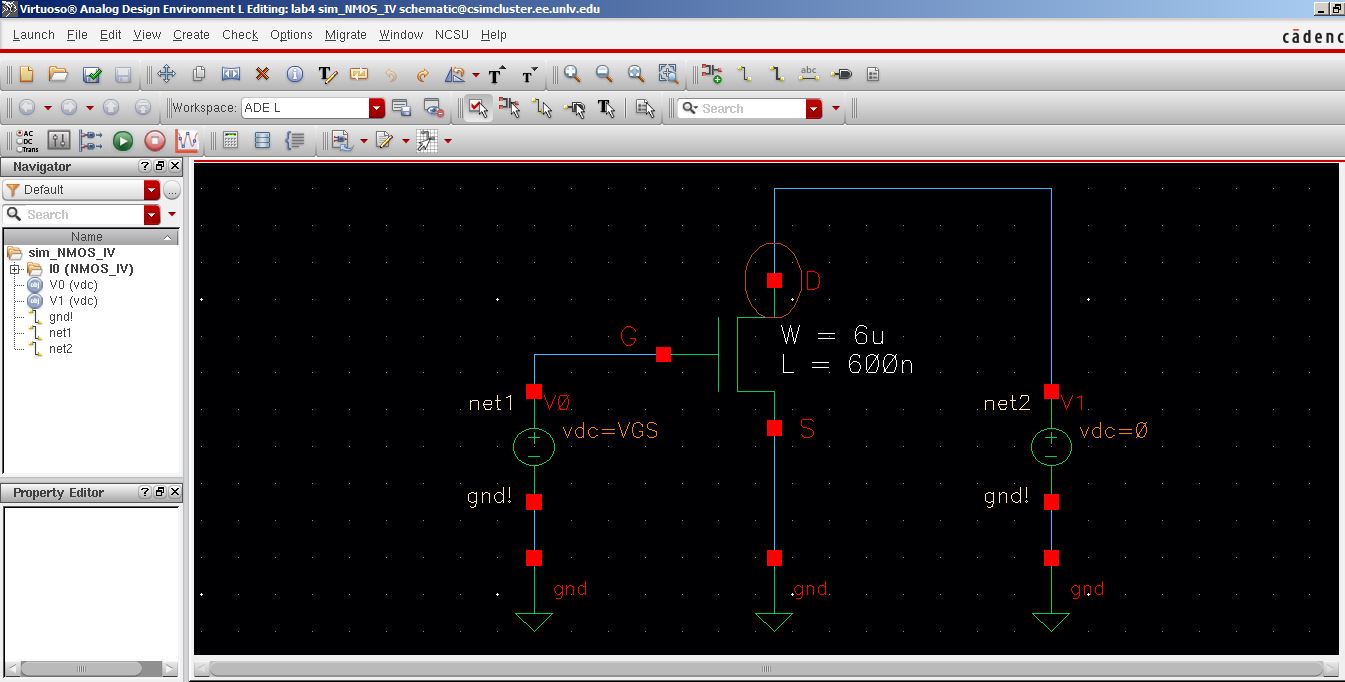
1. Schematic for simulating ID v. VDS of an NMOS device for VGS varying from 0 to 5 V in 1 V steps while VDS varies from 0 to 5 V in 1 mV steps. Use a 6u/600n width-to-length ratio.
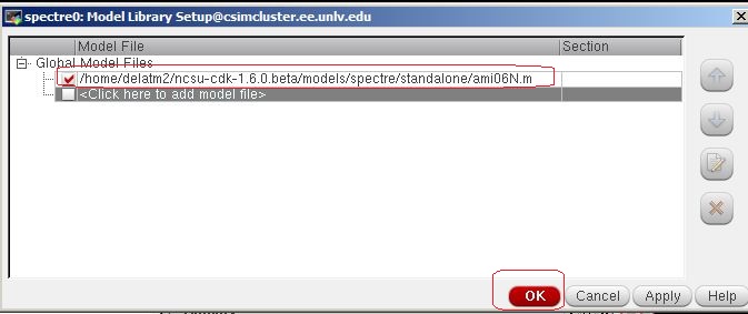
Simulation and settings.

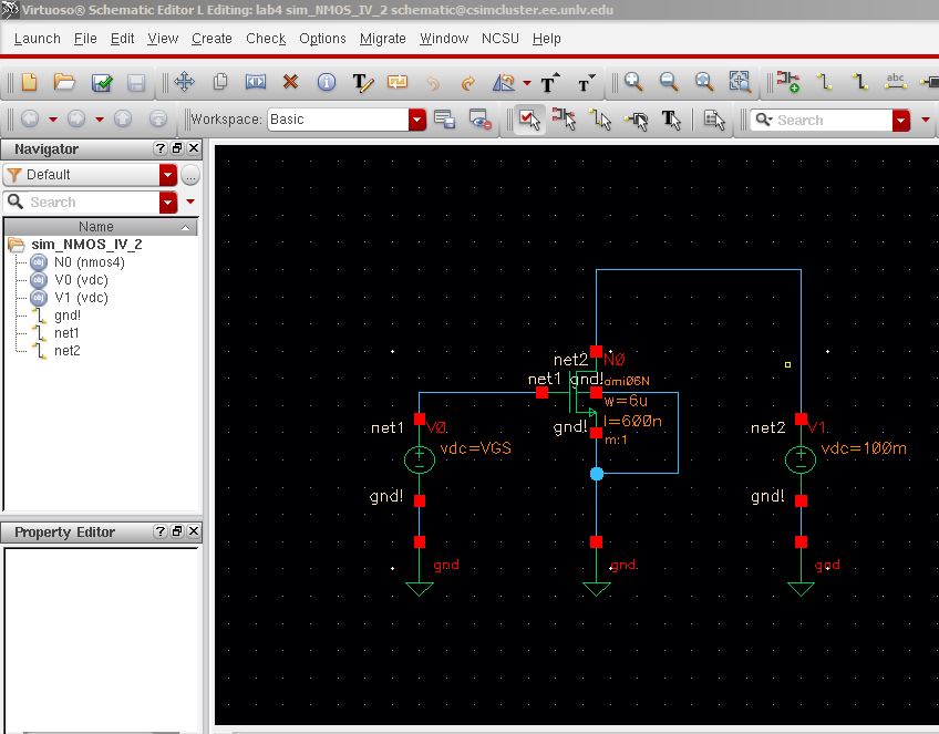
2. Schematic for simulating ID v. VGS of an NMOS device for VDS = 100 mV where VGS varies from 0 to 2 V in 1 mV steps. Again use a 6u/600n width-to-length ratio.
Simulation and settings.

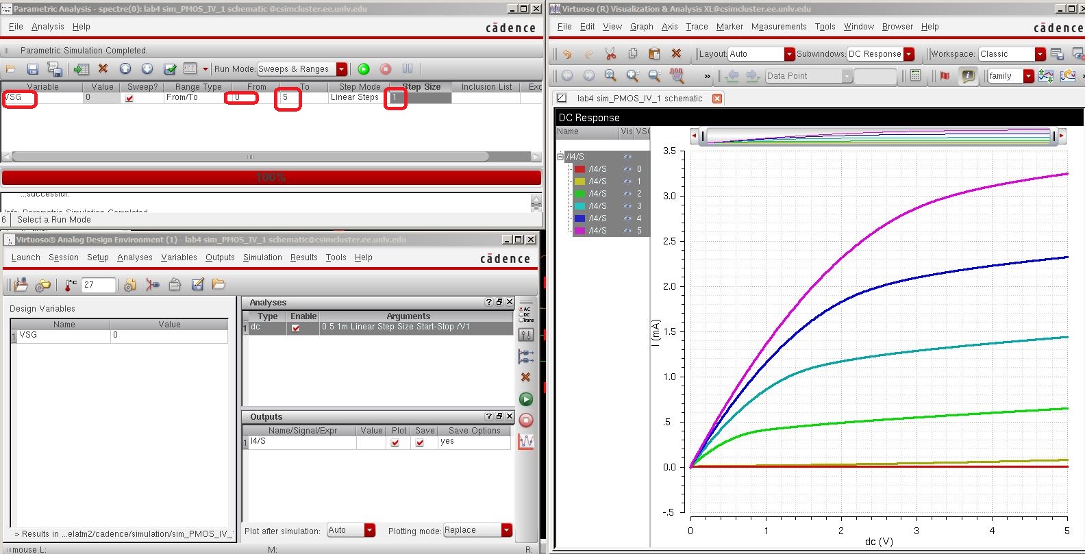
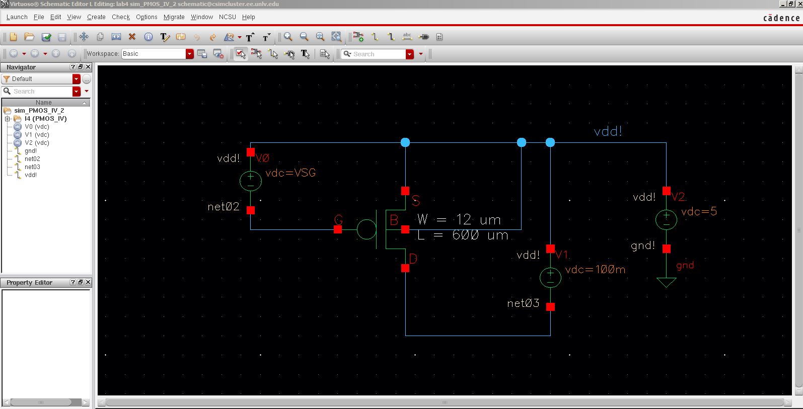
3. Schematic for simulating ID v. VSD (note VSD not VDS) of a PMOS device for VSG (not VGS) varying from 0 to 5 V in 1 V steps while VSD varies from 0 to 5 V in 1 mV steps. Use a 12u/600n width-to-length ratio.

Simulation and settings. Notice that the current is positive since the measurement was taking for the source of the device.
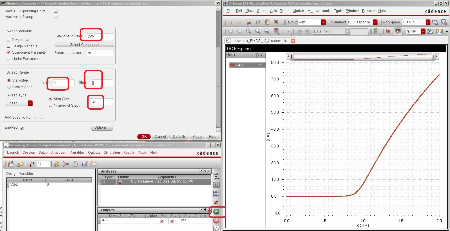
4. Schematic for simulating ID v. VSG of a PMOS device for VSD = 100 mV where VSG varies from 0 to 2 V in 1 mV steps. Again, use a 12u/600n width-to-length ratio.
Simulation and settings. Notice that the current is positive since the measurement was taking for the source of the device.
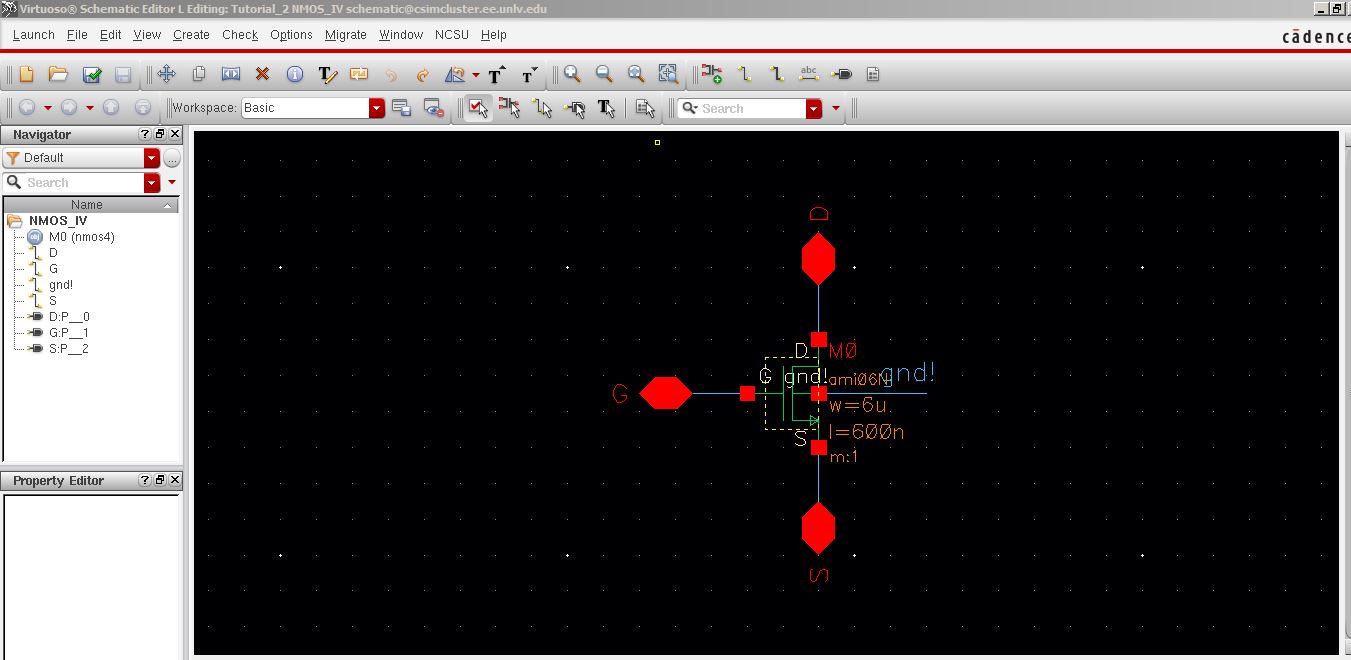
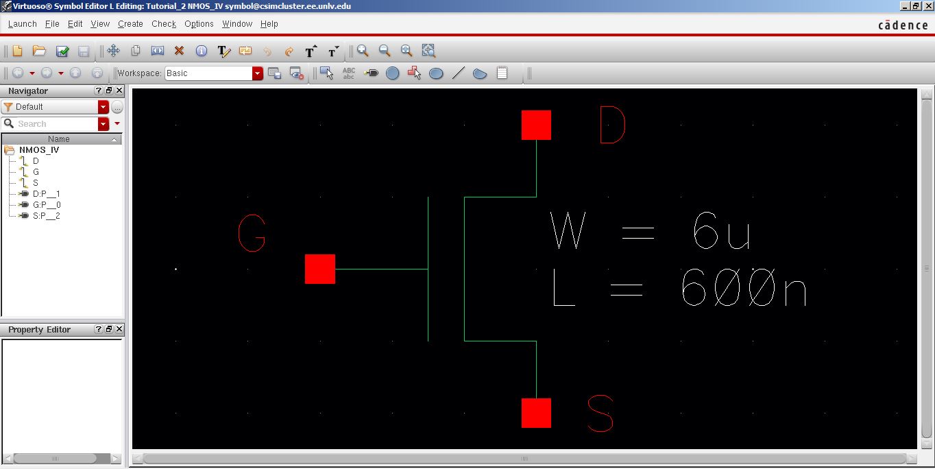
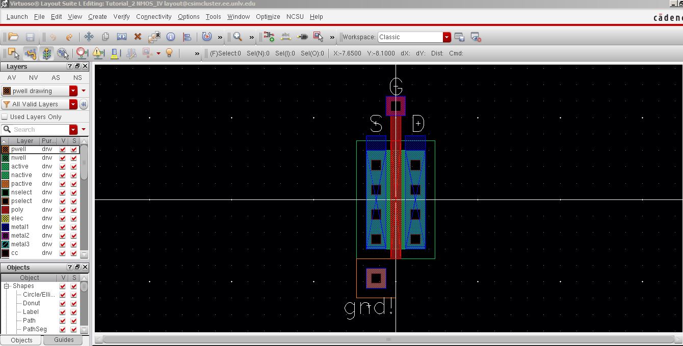
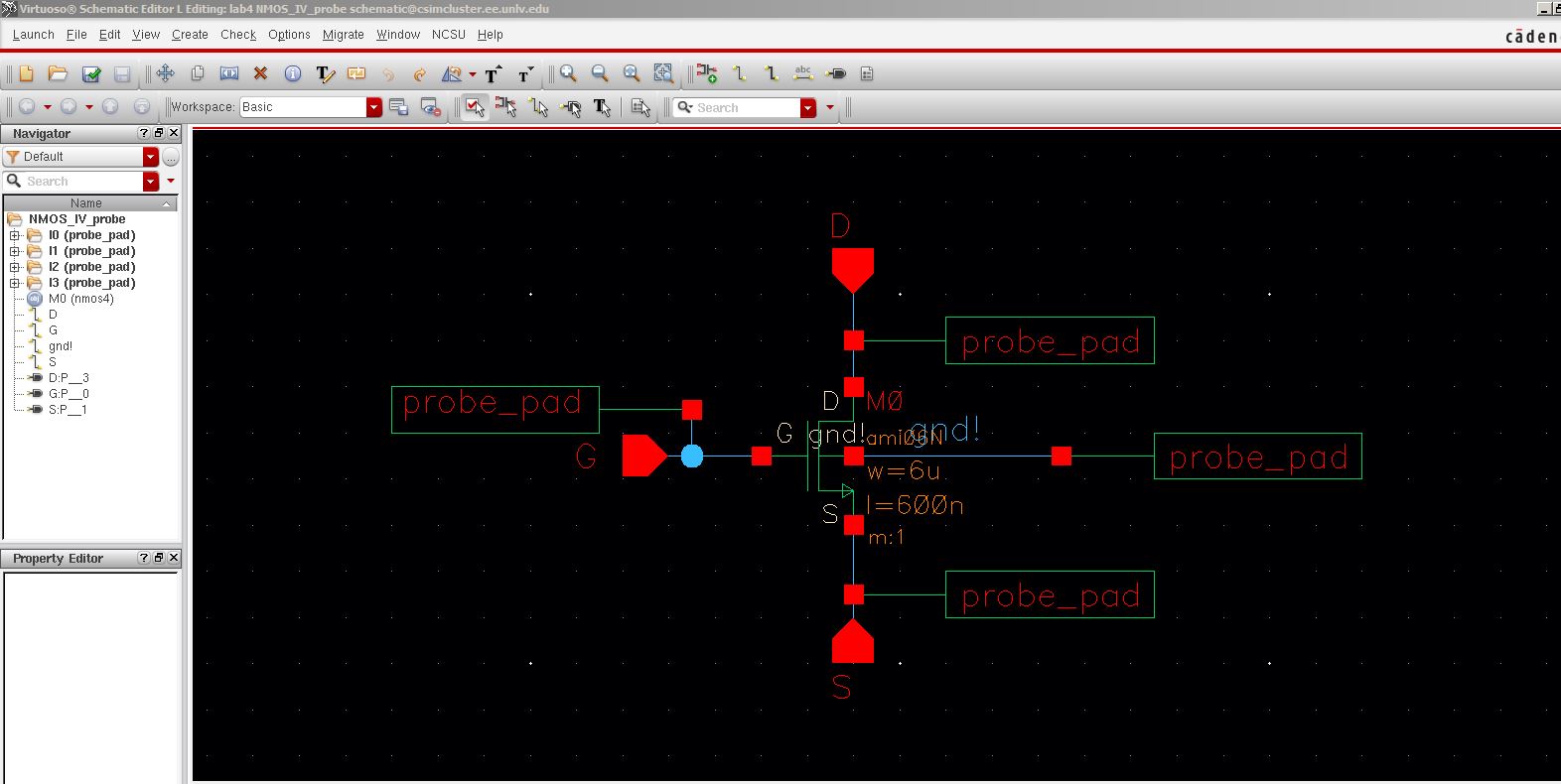
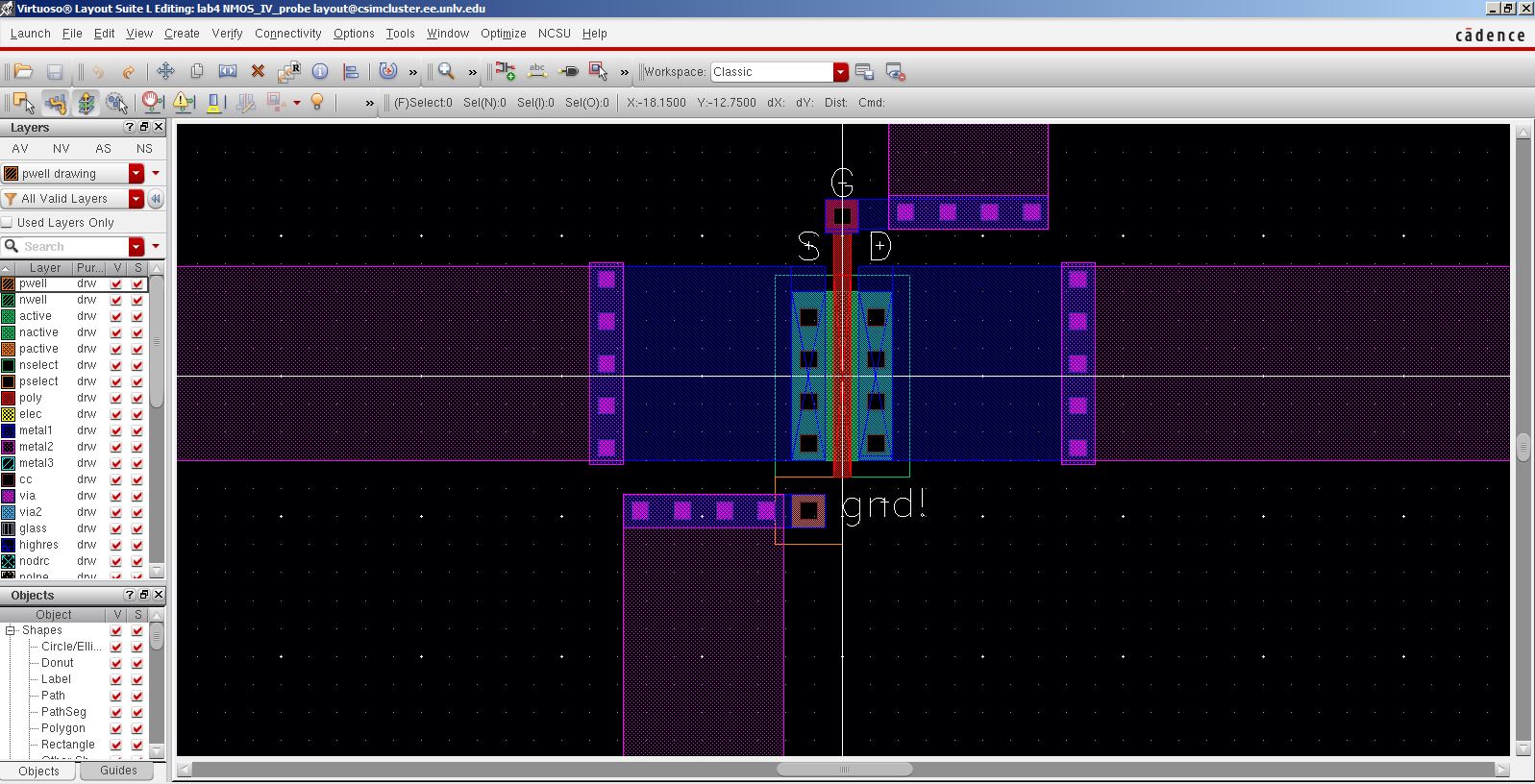
5. A 6u/0.6u NMOS device and connect all 4 MOSFET terminals to probe pads.
a. Schematic.
b. Symbol.

c. Layout and DRC.
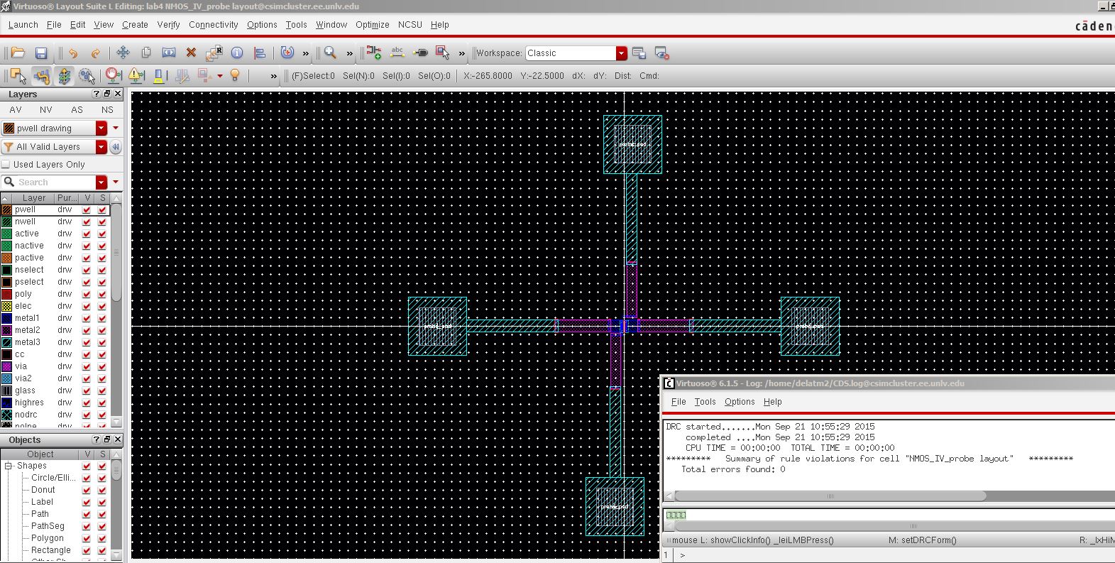
Closeup view.
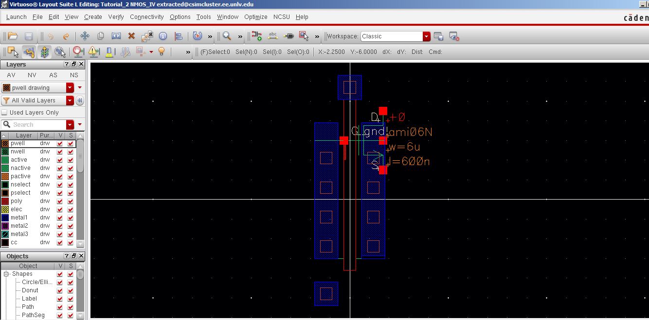
d. Extracted view showing the device and L/W.

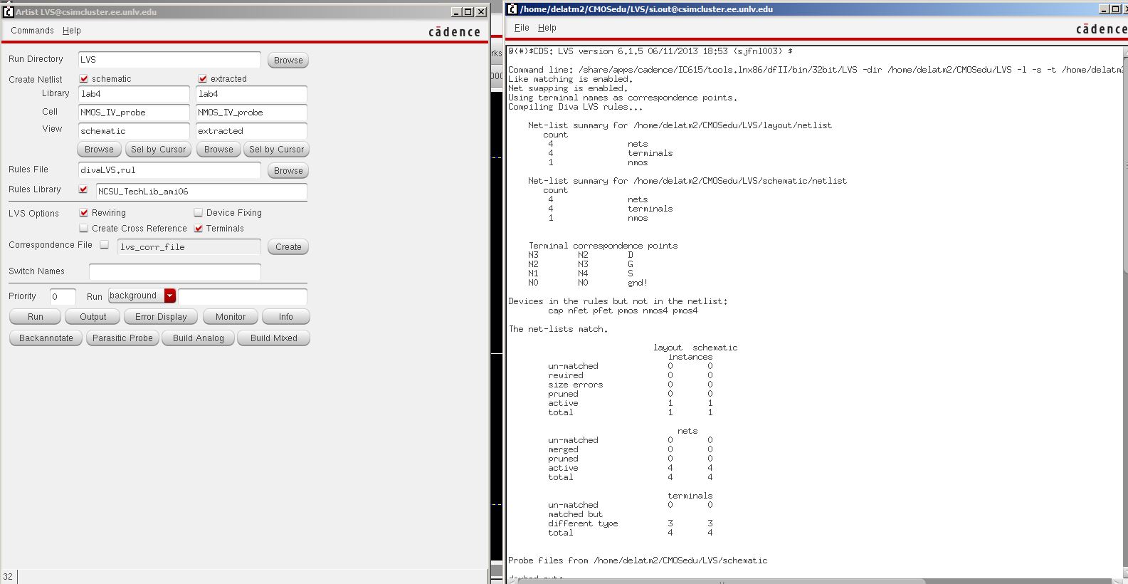
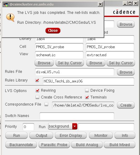
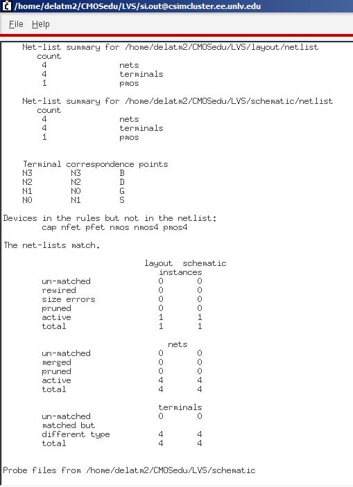
e. LVS report.
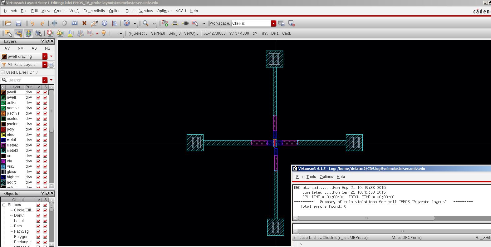
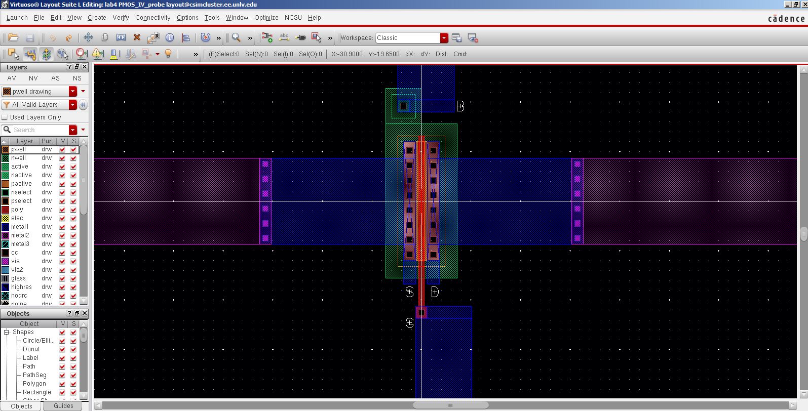
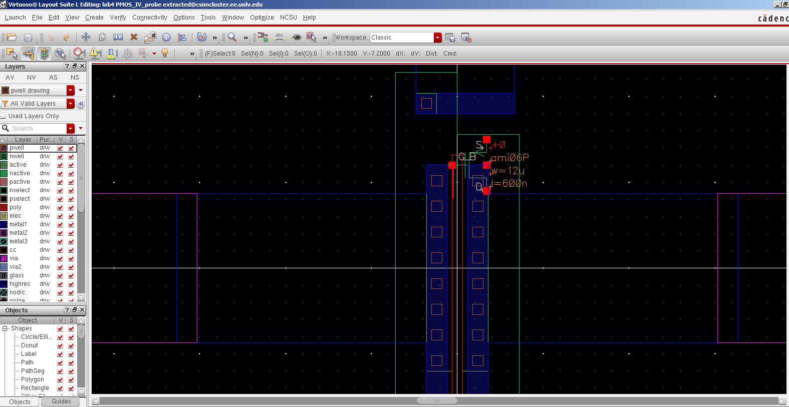
6. A 12u/0.6u PMOS device and connect all 4 MOSFET terminals to probe pads.
a. Schematic.

b. Symbol.

c. Layout and DRC.
Closeup.
d. Extracted view showing the device and L/W.
Backing up my work.
e. LVS report.
Backing up my work.
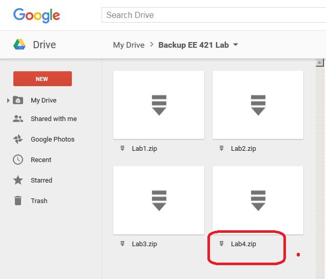
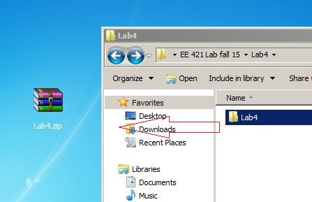
1. A zip folder will be created Lab2.
2. Then the zipped folder will be store on my google drive.