Lab 3 - EE 421L Fall 2015
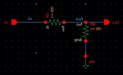
1. We started out by removing the voltage source and adding pins to the input and output of the circuit.
2. Once the in and out pins were added, a symbol was created from the cellview.
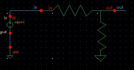
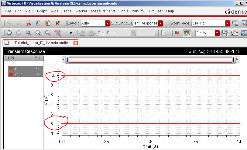
3. Simulation using the symbol. As expected the output was the same.
4. Using the n-well to layout the resistive divider.
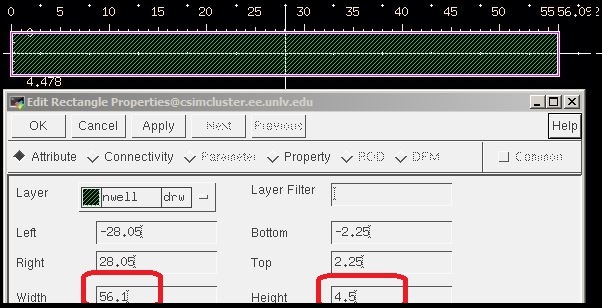
a. Layout of the n-well. The calculated dimensions
for the 10k resistor are width = 4.5 um and length = 56.1.
b. Adding the ntaps to the ends of the n-well resistor.
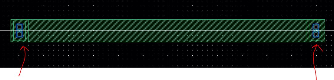
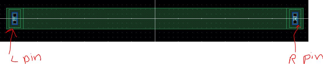
c. Adding the pins to the layout.
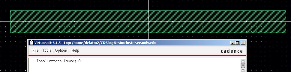
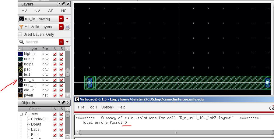
d. The layer res_id was used to identify the 10k resistor. Also the layout was DRC and fournd 0 errors.
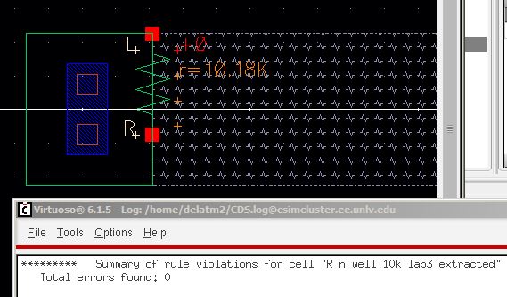
e. Finally the layout was extracted and the value of the 10k resistor was verified.
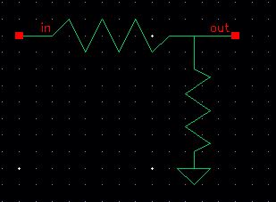
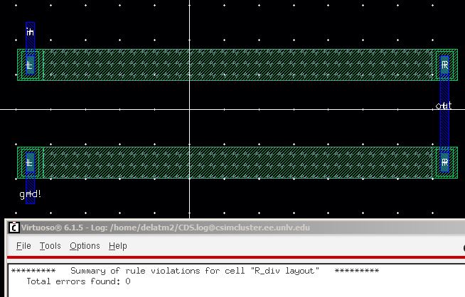
5. Drawing the layout of the R_div cell. After the 2 10k resistors were instanced and the pins were added (in, out, and gnd!) we have the following:
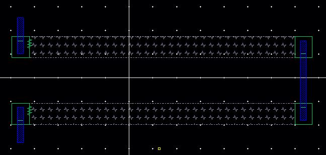
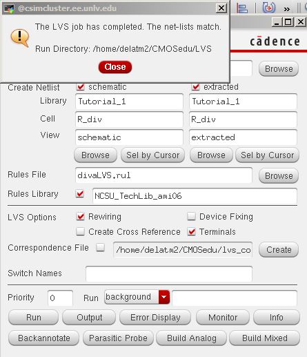
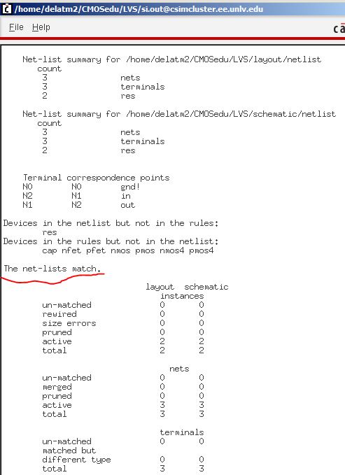
6. Finally the extraced view and the LVS report.
LVS
This concludes tutorial 1.
Post-Lab
1. Use the n-well to layout a 10k resistor as discussed in Tutorial 1.
a. The formula to calculate the resistance is R = Rsqr*L/W. Using this formula The calculated dimensions for the 10k resistor are width = 4.5 um and length = 56, but following the MOSIS design rules 56 is not divisible by 0.15 so the actual length was increase to 56.1. The ruler (bindkey k) is used to measure the length and width of the n-well. The length and width are also obtained by selecting the n-well the pressing "q" to display the properties of the element.
2. An n-well resistor was used to layout the DACbit. Pins In, Top and Bottom were added to match the schematic.
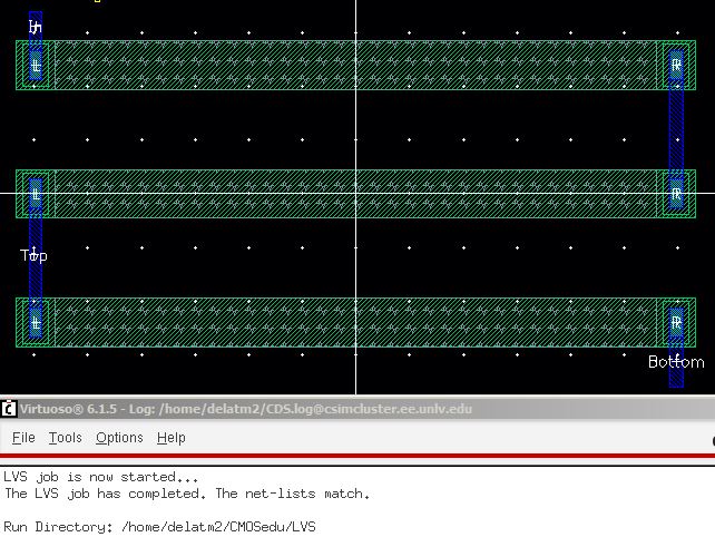
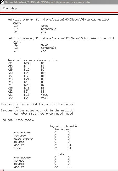
LVS report DACbit.
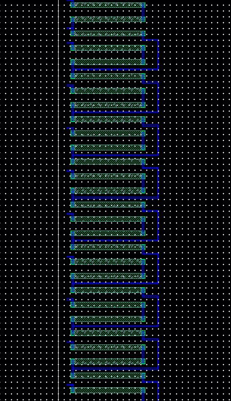
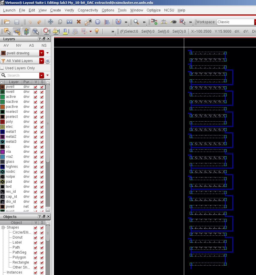
3.Using 10 of the DACbit stacked together made the 10-bit DAC plus an extra 10k resistor connected to ground..
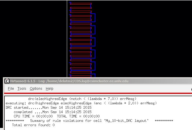
DRC report
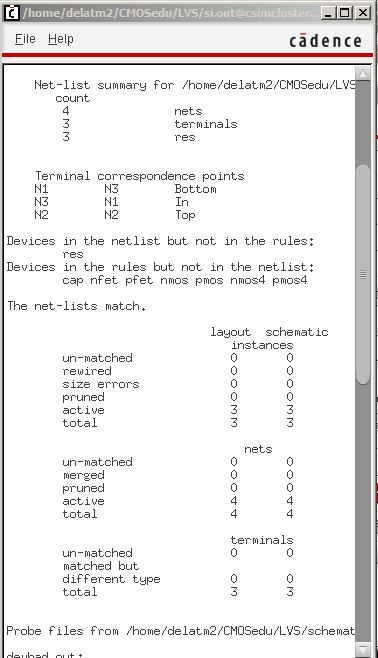
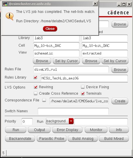
LVS report 10-bit DAC.
Extracted view.
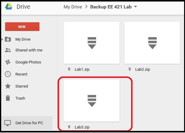
Backing up my work.
1. A zip folder will be created Lab3.
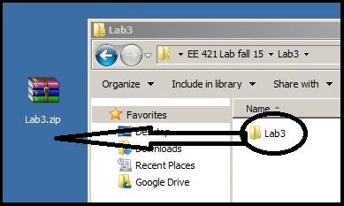
2. Then the zipped folder will be store on my google drive.