Lab 2 - EE 421L Fall 2015

Design of a 10-bit digital-to-analog converter (DAC)

Mario De La Torre

delatm2@unlv.nevada.edu

8/29/2015 

  Pre-lab


1.  Download lab2.zip to your desktop. This contains a simulation example using an ideal 10-bit Analog-to-Digital Converter (ADC) and Digital-to-Analog Converter (DAC).


http://cmosedu.com/jbaker/courses/ee421L/f15/students/delatm2/Lab2/pic1_dwnld.JPG


2. Upload this zip file to the design directory on Cadence.


http://cmosedu.com/jbaker/courses/ee421L/f15/students/delatm2/Lab2/pic2_upload.JPG


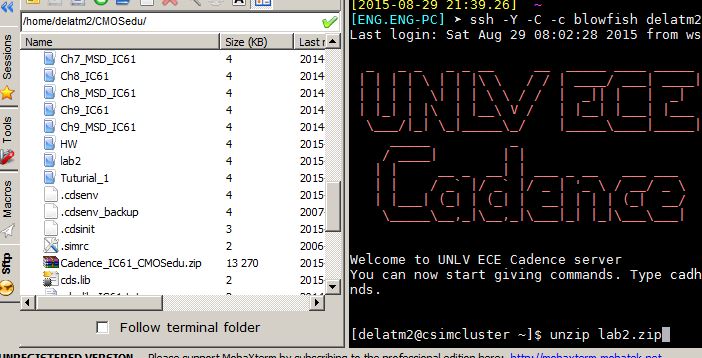
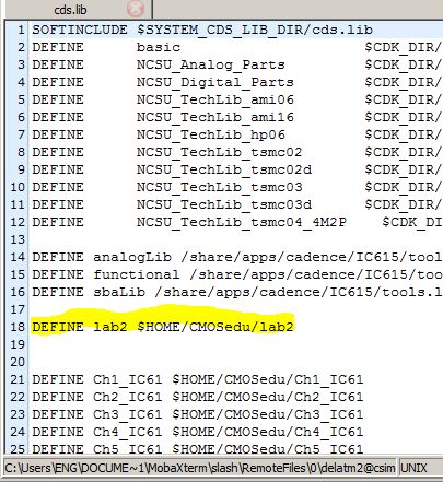
3. Unzip this directory and add, to your cds.lib in the design directory, the following statement:  DEFINE lab2 $HOME/CMOSedu/lab2.


http://cmosedu.com/jbaker/courses/ee421L/f15/students/delatm2/Lab2/pic3_unzip.JPG


 http://cmosedu.com/jbaker/courses/ee421L/f15/students/delatm2/Lab2/pic4_cdslib.JPG


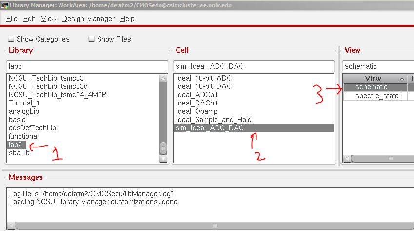
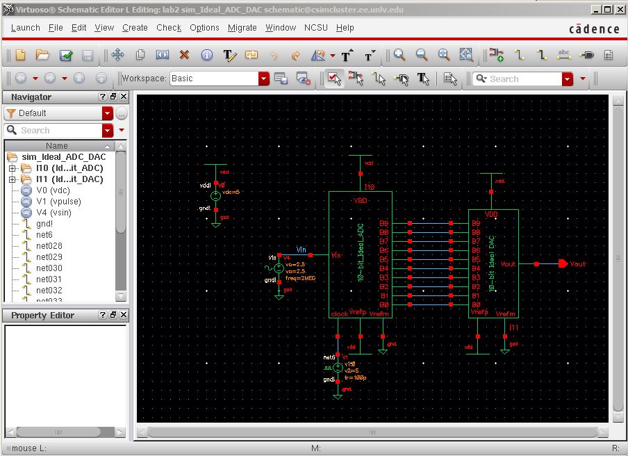
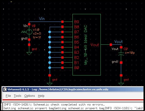
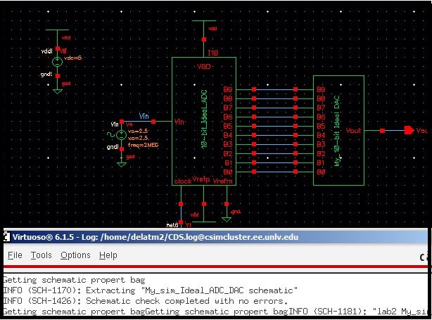
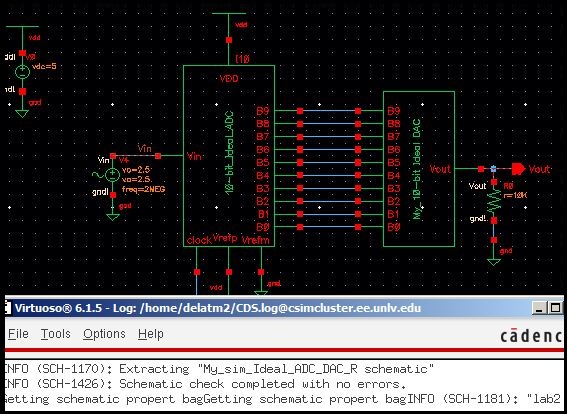
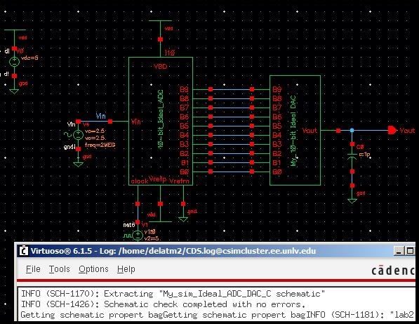
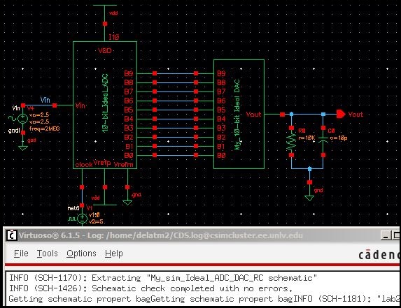
4.  Once Cadence is running, use the Library Manager and navigate to the lab2 library, then open the schematic view of the cell sim_Ideal_ADC_DAC.


http://cmosedu.com/jbaker/courses/ee421L/f15/students/delatm2/Lab2/pic5_openfile.JPG


Schematic.


http://cmosedu.com/jbaker/courses/ee421L/f15/students/delatm2/Lab2/pic6_schematic.JPG


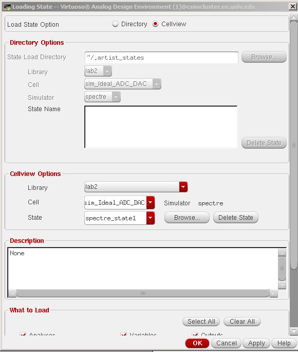
5. Run the simulation (Launch the ADE, Session -> Load State -> Cellview -> OK.


http://cmosedu.com/jbaker/courses/ee421L/f15/students/delatm2/Lab2/pic7_launchADE.JPG


http://cmosedu.com/jbaker/courses/ee421L/f15/students/delatm2/Lab2/pic8_loadstate.JPG


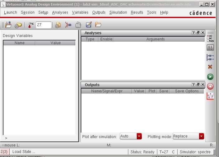
6. Run the simulation.


http://cmosedu.com/jbaker/courses/ee421L/f15/students/delatm2/Lab2/pic9_sim.JPG


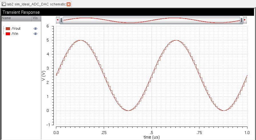
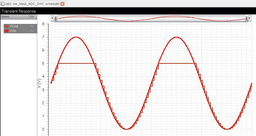
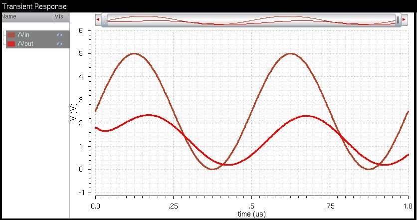
If the input sinewave execeeds the circuit's limits, in this case 5V, the output will be clipped.


 http://cmosedu.com/jbaker/courses/ee421L/f15/students/delatm2/Lab2/pic9_sim2_schem.JPG


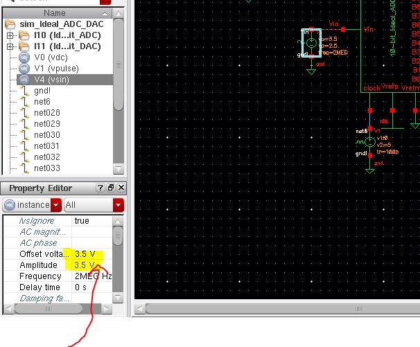
In this case the input was change from 5V to 7V.


 http://cmosedu.com/jbaker/courses/ee421L/f15/students/delatm2/Lab2/pic9_sim2.JPG


The equation to find the LSB is  1LSB=VDD/(2^n) were n is the number of bits of the DAC. In this example 1LSB= 5V/(2^10)= 4.88 mV.


Post-Lab

In this lab I'll use n-well resistors to implement a 10-bit DAC.
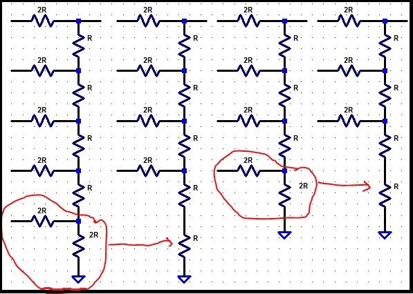
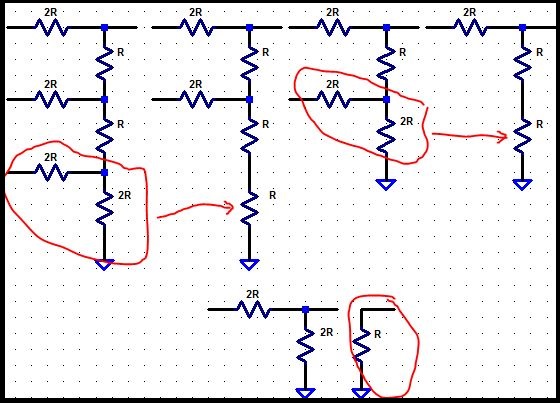
1. The design is based upon the topology seen in the following figure.  


http://cmosedu.com/jbaker/courses/ee421L/f15/students/delatm2/Lab2/post1_fig30_14.jpg


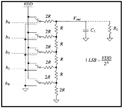
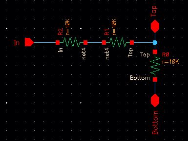
2. The output resitance of the DAC is determine by combining 2R||2R = R, then R + R = 2R and finally we get R for the  as seen in the picture:


http://cmosedu.com/jbaker/courses/ee421L/f15/students/delatm2/Lab2/post1_res_equ1.JPG


http://cmosedu.com/jbaker/courses/ee421L/f15/students/delatm2/Lab2/post1_res_equ2.JPG


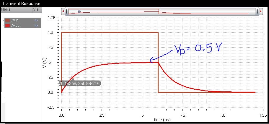
3. Using Td = 0.7*R*C, we can predict the delay of the DAC.  Td = 0.7*10k*10p= 70 ns.  Since Vp = 1*512/1024 = 500 mV and 50% of Vp is 250 mV.


http://cmosedu.com/jbaker/courses/ee421L/f15/students/delatm2/Lab2/post2_10bit_DAC_delay.jpg


http://cmosedu.com/jbaker/courses/ee421L/f15/students/delatm2/Lab2/post2_10bit_DAC_delay_sim.jpg


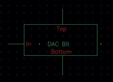
4.  To create the a symbol view for the design using the exact same footprint as the Ideal_10-bit_DAC symbol view.  


    a. A copy of the cell Ideal_DACbit was re-name My_Ideal_DACbit and the shematic was replace with this circuit.


http://cmosedu.com/jbaker/courses/ee421L/f15/students/delatm2/Lab2/post7_sch_DACbit.JPG


Then a new symbol was created from the circuit


http://cmosedu.com/jbaker/courses/ee421L/f15/students/delatm2/Lab2/post7_sym_DACbit.JPG


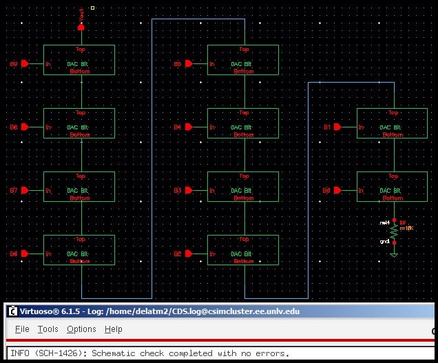
    b. Once the DAC bit was created, a copy of the Ideal_10-bit_DAC was made and renamed My_Ideal_10-bit_DAC.  By using the DAC bit symbols this circuit was made.


http://cmosedu.com/jbaker/courses/ee421L/f15/students/delatm2/Lab2/post4_10-bit_DAC.JPG


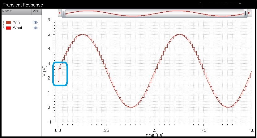
5. Simulations and verification of the circuit.  The output was almost identical except for the blue circle on the waveform.


http://cmosedu.com/jbaker/courses/ee421L/f15/students/delatm2/Lab2/post6_sim_10-bit_DAC_schem.JPG


http://cmosedu.com/jbaker/courses/ee421L/f15/students/delatm2/Lab2/post5_10-bit_DAC_sym2.JPG


6. Circuit driving different loads.


    a. The DAC driving a R load.  The output of the DAC is about half of the input because the 10k resistor load is connected in series with the 10k equivalent resistance of the DAC circuit.  It is acting like a voltage divider with a ratio of 0.5.


    http://cmosedu.com/jbaker/courses/ee421L/f15/students/delatm2/Lab2/post10_10-bit_DAC_R_schem.JPG


    http://cmosedu.com/jbaker/courses/ee421L/f15/students/delatm2/Lab2/post10_sim_10-bit_DAC_R.JPG


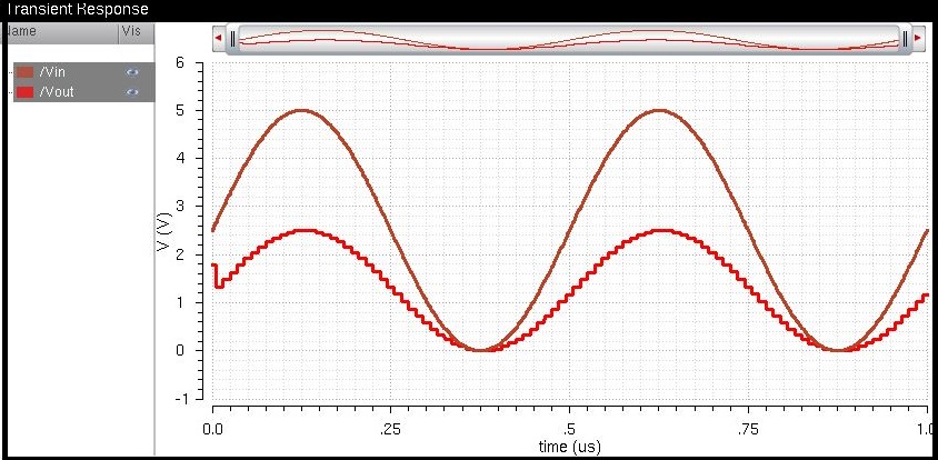
    b. With the capacitor the output it's smoother but less amplitude because the capactive reactance (Xc).


    http://cmosedu.com/jbaker/courses/ee421L/f15/students/delatm2/Lab2/post11_10-bit_DAC_C_schem.JPG


    http://cmosedu.com/jbaker/courses/ee421L/f15/students/delatm2/Lab2/post11_sim_10-bit_DAC_C.JPG


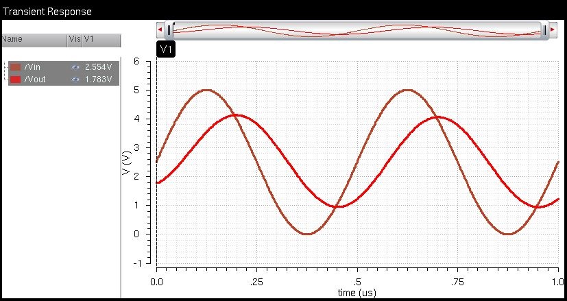
    c. With the  RC load the output is even less because the combination of the copacitor and resistor.


    http://cmosedu.com/jbaker/courses/ee421L/f15/students/delatm2/Lab2/post12_10-bit_DAC_RC_schem.JPG


    http://cmosedu.com/jbaker/courses/ee421L/f15/students/delatm2/Lab2/post12_sim_10-bit_DAC_RC.JPG


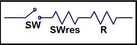
In a real circuit the switches seen above (the outputs of the ADC) are implemented with transistors (MOSFETs).  If the resistance of the switches is not small compared to the resistance of the voltage divider circuit, the output voltage of the DAC will be less because there will be a voltage drop across SWres.
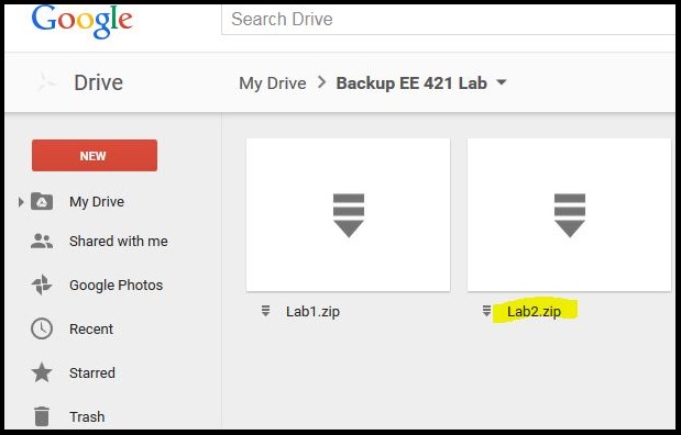
 

http://cmosedu.com/jbaker/courses/ee421L/f15/students/delatm2/Lab2/SWres.JPG


Backing up my work.

1. A zip folder will be created Lab2.


http://cmosedu.com/jbaker/courses/ee421L/f15/students/delatm2/Lab2/pic10_zip.JPG


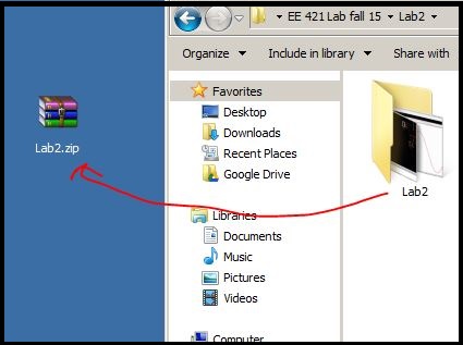
2. Then the zipped folder will be store on my google drive.


http://cmosedu.com/jbaker/courses/ee421L/f15/students/delatm2/Lab2/pic11_googledrive.JPG

Return to delatm2 lab directory


Return to EE 421L Labs