- A schematic for simulating ID v. VDS of an NMOS device for VGS varying from 0 to 5 V in 1 V steps while VDS varies from 0 to 5 V in 1 mV steps. Use a 6u/600n width-to-length ratio.
- A schematic for simulating ID v. VGS of an NMOS device for VDS = 100 mV where VGS varies from 0 to 2 V in 1 mV steps. Again use a 6u/600n width-to-length ratio.
- A schematic for simulating ID v. VSD (note VSD not VDS) of a PMOS device for VSG (not VGS) varying from 0 to 5 V in 1 V steps while VSD varies from 0 to 5 V in 1 mV steps. Use a 12u/600n width-to-length ratio.
- A schematic for simulating ID v. VSG of a PMOS device for VSD = 100 mV where VSG varies from 0 to 2 V in 1 mV steps. Again, use a 12u/600n width-to-length ratio.


The first image is a of the schematic used to simulate the current and voltage characteristics of the NMOS. The second image provides a parametric analysis in which VGS (gate-source voltage) is being swept from 0 - 5 V in 1 volt increments. Also VDS (drain-source voltage) is being swept from 0 to 5 V in 1 milli-volt increments.
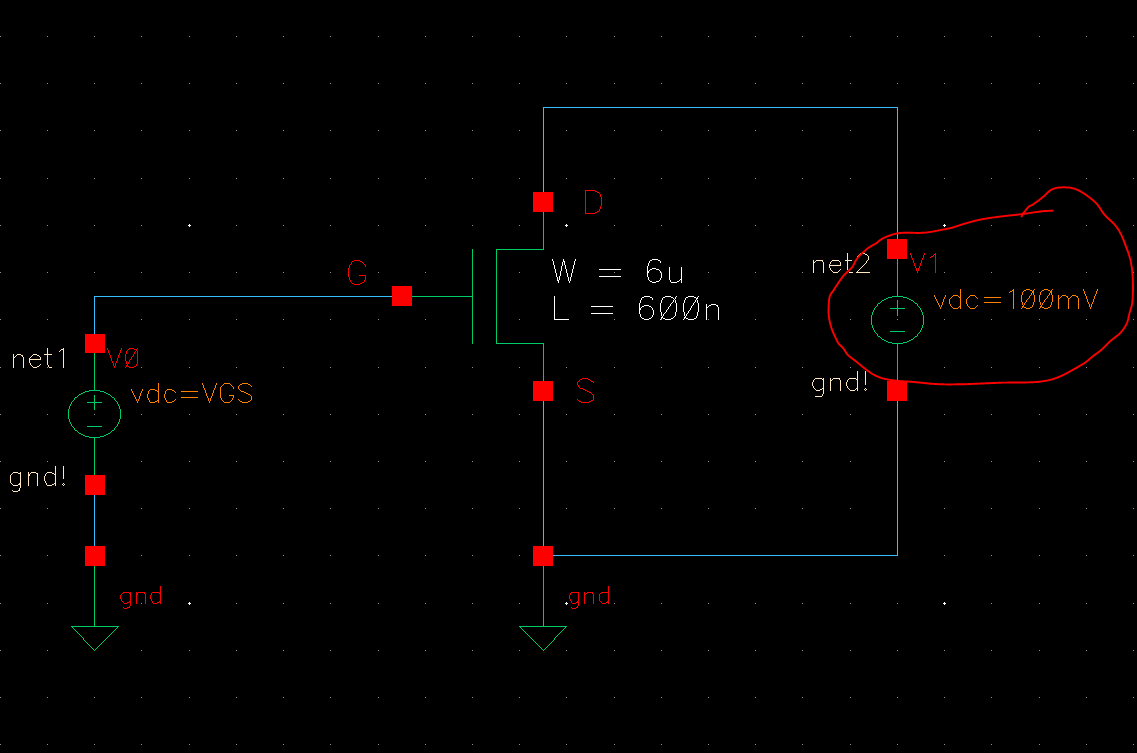
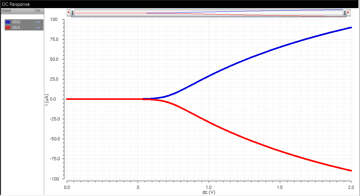
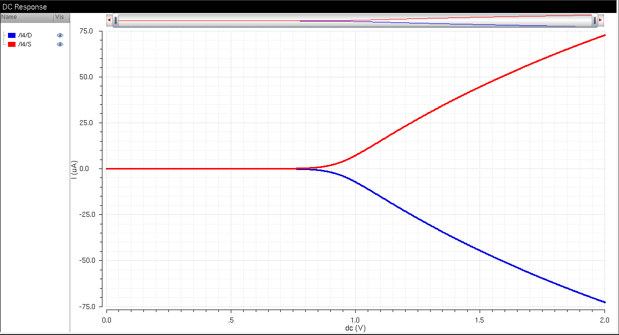
The first image is a of the schematic used to simulate the current and voltage characteristics of the NMOS. The difference between this simulation and the previous one is the fact that VDS remains constant at 100 mV. In the second image, a transient anaylis is being performed on the provided circuit. Notice how the source and drain currents behave in a contradicting manner.
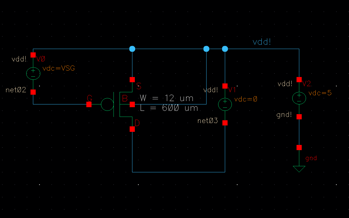
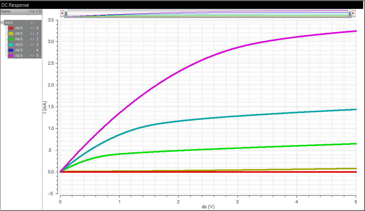
The first image is a of the schematic used to simulate the current and voltage characteristics of the PMOS. The second image provides a parametric analysis where VSG (source-gate voltage) is being swept from 0 to 5 volts in 1 volt increments. Also, VSD (source-drain voltage) is being swept from 0 - 5 V in 1 mV steps.

The first image is a of the schematic used to simulate the current and voltage characteristics of the PMOS. Here VSD remains constant at 100 mV while VSG is being swept from 0 to 2 volts in 1 mV increments. Similar to the NMOS, the drain and source currents are reflected about the x-axis.
- Show your layout passes DRCs.
- Make a corresponding schematic so you can LVS your layout.
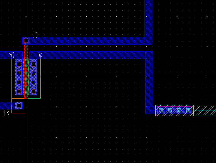

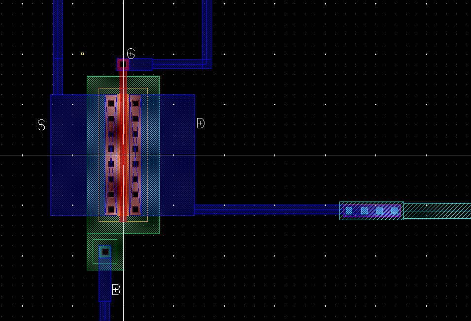
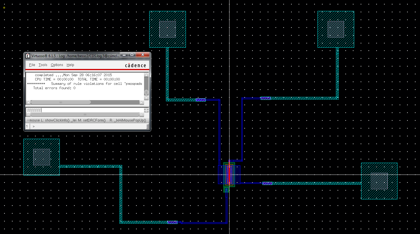
The first image shows a zoomed view of the layout, focusing on the NMOS. The second image shows that the layout passed the DRC checks.
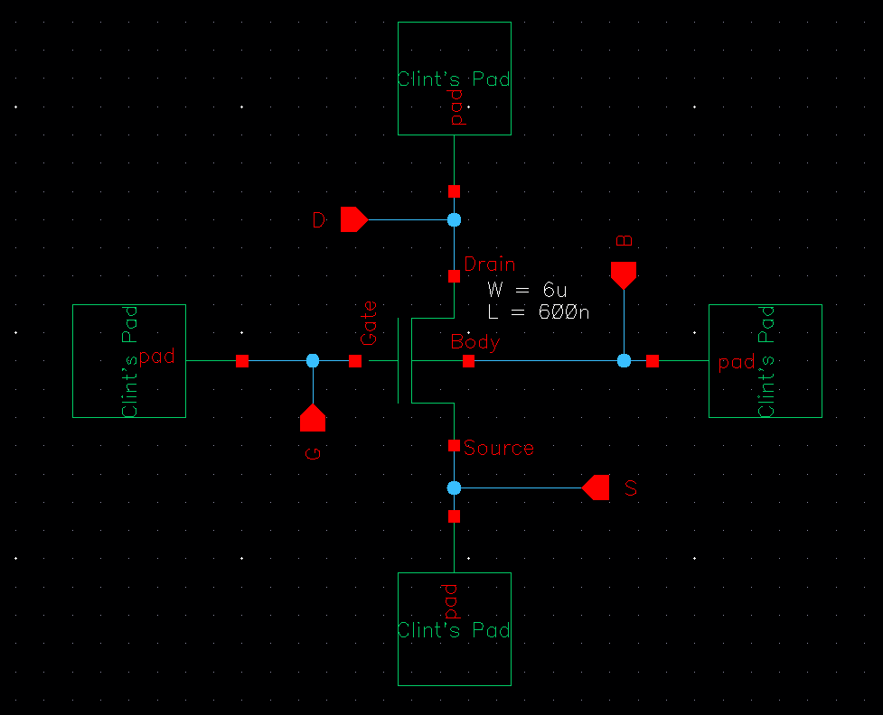

The first image shows the schematic along with the pads that are connected. The second image shows the full layout and the completion of the LVS.
- Show your layout passes DRCs.
- Make a corresponding schematic so you can LVS your layout.
The first image shows a zoomed view of the layout, focusing on the PMOS. The second image shows that the layout passed the DRC checks.


The first image shows the schematic along with the pads that are connected. The second image shows the full layout and the completion of the LVS.
