- Discuss, in your lab report, how to select the width and length of the resistor by referencing the process information from MOSIS
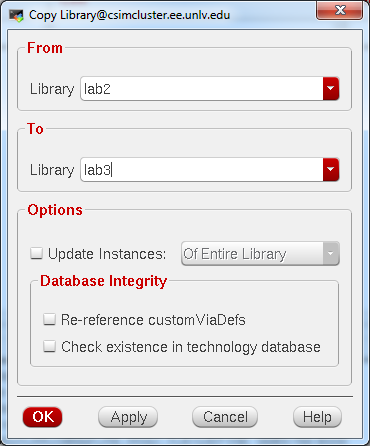
The first thing I did was copied the contents of the lab2 directory to the lab3 directory. By doing this I saved a lot of time by not having to recreate a few symbols and layouts. In regards to the creation of the 10k resistor, I first took into account theat the n-well process uses a sheet resistance of 800 ohms per square. 10k ohms / 800 ohms per square provides 12.5 squares. If we are using a lambda of 300 nn, the C5 MOSIS process requries a minimum width well of 12 lambda and a well spacing of 18 lambda. In turn, the minimum length is 45 um and the minimum with is 3.6 um.
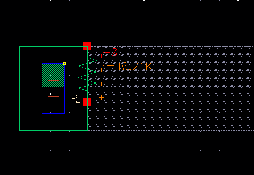
Here is an image of the extracted n-well resistor. I used a total length of 45 um and a total width of 3.6 um. Even though we wanted 10k ohms the actual result came out to be 10.21k ohms, which is still acceptable
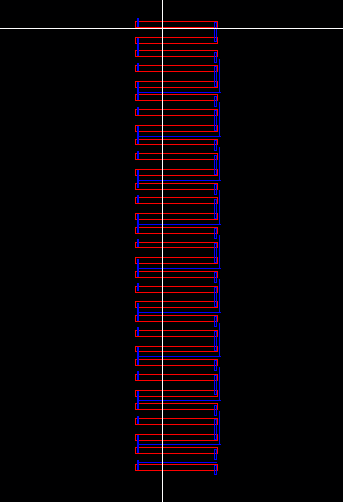

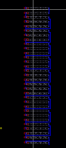
Here I created a layout by using a serpentine connection of to route all of the nodes.
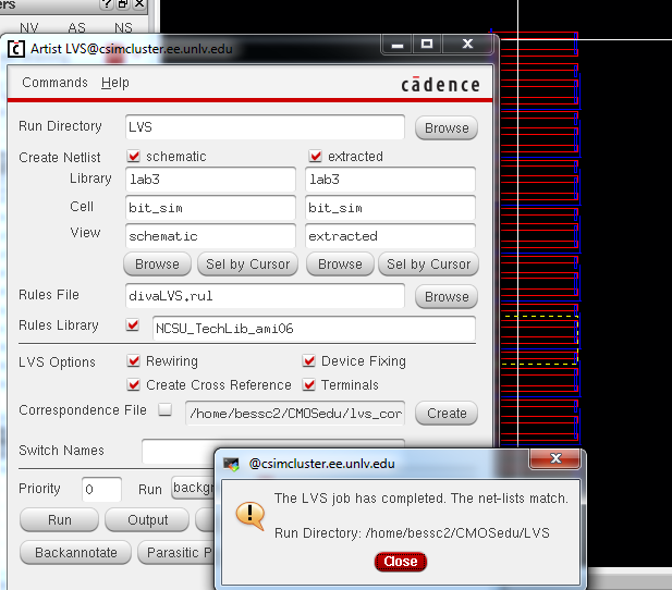

The first image shows that the layout succeeded in running LVS. The next two images show the extracted views of the layout.


After extracting the layout I opened up the simulation schematic. Here are the results. Notice how they are similar to the simulations in the pre-lab
