Lab 8 - ECE 421L
Authored
by Silvestre Solano, Nha Tran, John Huangj
Email: Solanos3@unlv.nevada.edu
trann4@unlv.nevada.edu
huangj19@unlv.nevada.edu
The
purpose of this lab is to implement at least the following test
structures on a standard 40 pad chip frame. The first task for chip
testing is a visual inspection to see if there are any obvious
imperfections. To test the chip, the chip must be hooked up to
proto board which will then be connnected to an oscilloscope
probe. To test any of the resistors, the resistors will have its
resistance measured with a multimeter. To test the 61 stage oscillator,
a square wave will be input to the oscillator and the output will be
observed. To test the VDD, an input voltage will be input and it will
be gradually increased from 0 to 5 volts and the current will be
measured. If the current exceed the expected value, then a short
circuit may be present.
- 30u/0.6u NMOS (3 pins,
DN, GN, SN, connect the p+ body, B, of the NMOS to the chip's ground
pin)
- 30u/0.6u PMOS (4 pins,
DP, GP, SP, and BP)
- Inverter made using 30u/0.6u NMOS and 60u/0.6u PMOS (3 pins, in, out, VDD_inv)
- 61 stage ring
oscillator using 6u/0.6u MOSFETs with off-chip buffer (2 pins, VDD_osc and Ocs_out. Ground connected to pin
20)
- 20k n-well resistor (2
pins)
- 20k hi-res poly
resistor (2 pins)
- 1k n+ resistor (2 pins)
- 1k p+ resistor (3
pins, need n-well to isolate the p+ from the p-substrate and the n-well
needs to be tied to a voltage >= either side of the resistor)
- Bandgap reference (2 pins, VDD_bg and Vref)
The chip frame diagram is shown below.
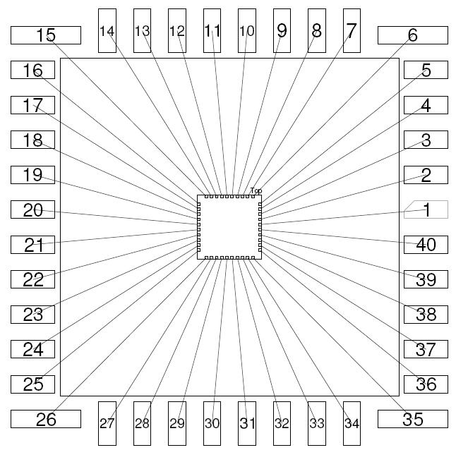
The test structures with their corresponding pin numbers are shown in the table below.
| 1)DN | 11) VDD_osc | 21) | 31) |
| 2)GN | 12) OCS_Out | 22) | 32) |
| 3)SN | 13) 20K nwell | 23) | 33) |
| 4) DP | 14) 20K hires | 24) | 34) |
| 5) GP | 15) 1K N+ | 25) | 35) |
| 6) SP | 16) 1K P+ | 26) | 36) |
| 7) BP | 17) P+ VDD | 27) | 37) |
| 8) out | 18) VDD_bg | 28) | 38) |
| 9) in | 19) Vref | 29) | 39) |
| 10) VDD_inv | 20) gnd! | 30) | 40) |
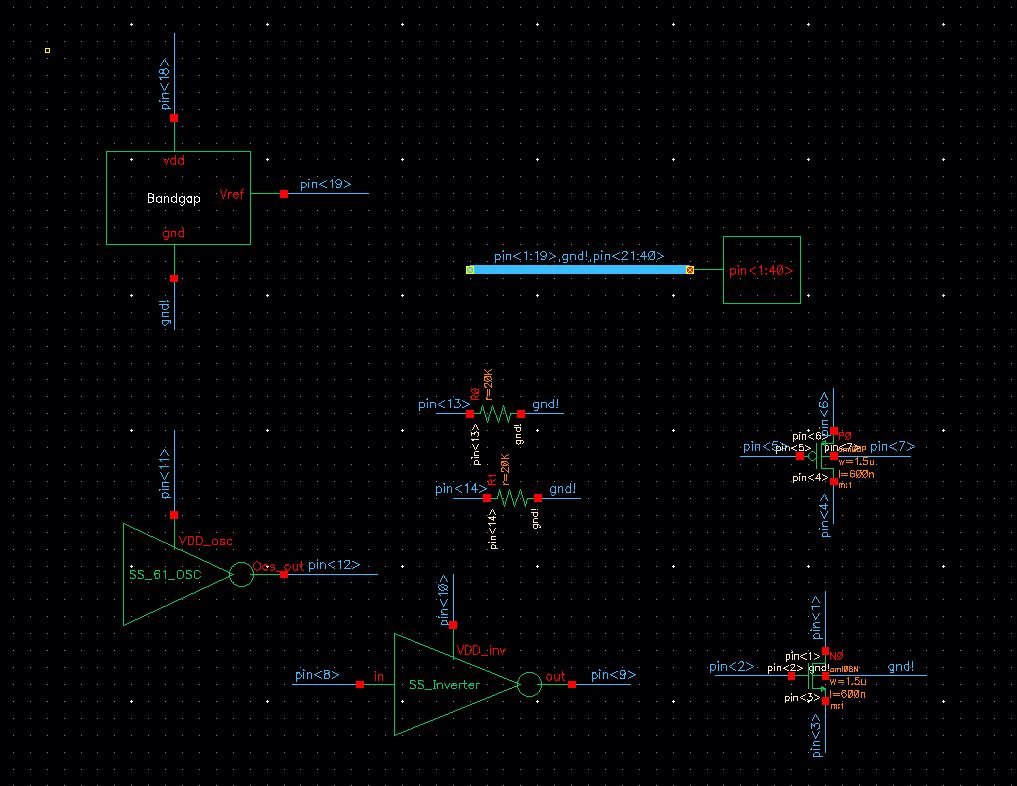
The
completed chip schematic is shown below. The p+ and n+ resistors are
not shown in the schematic because the layout would not LVS properly.
The p+ and n+ resistors are covered with the nodrc layer.
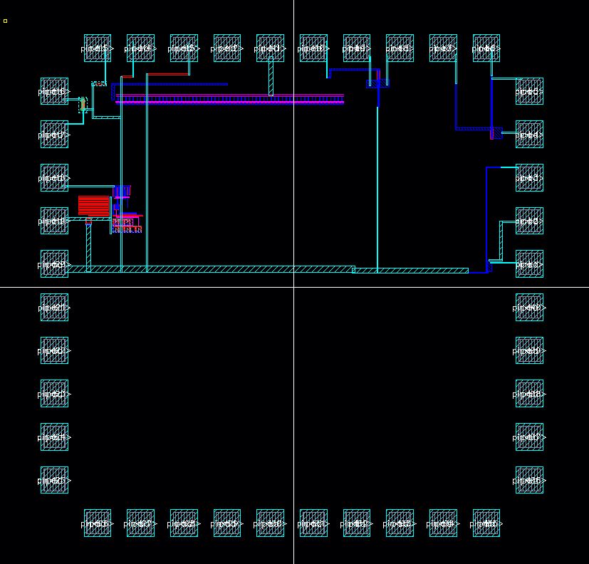
The layout is shown below.
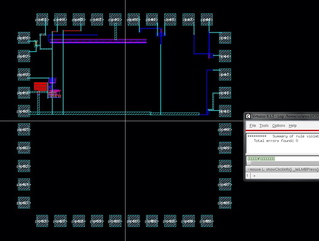
The successful DRC of the layout is shown below.
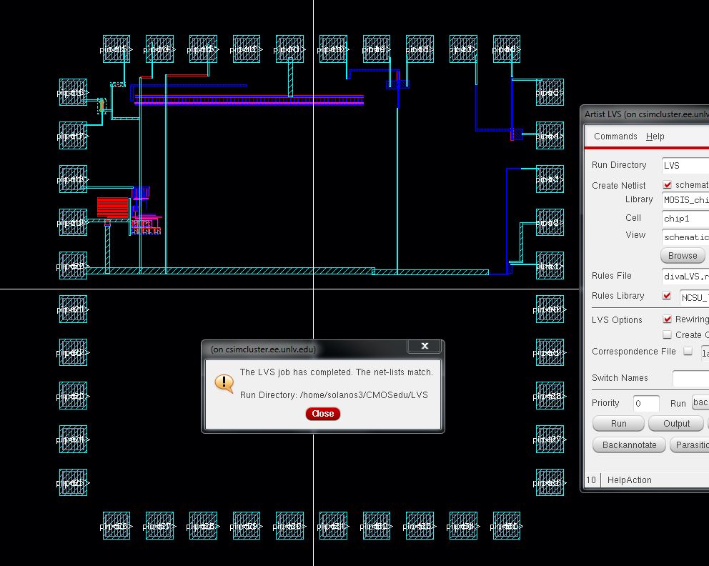
The succesfull LVS is shown below.
The layout of the poly2 resistor is shown below.
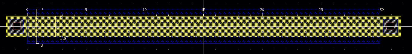
The layout of the nwell resistor is shown below.

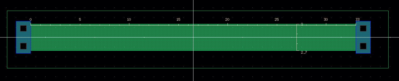
The layout of the n+ resistor is shown below
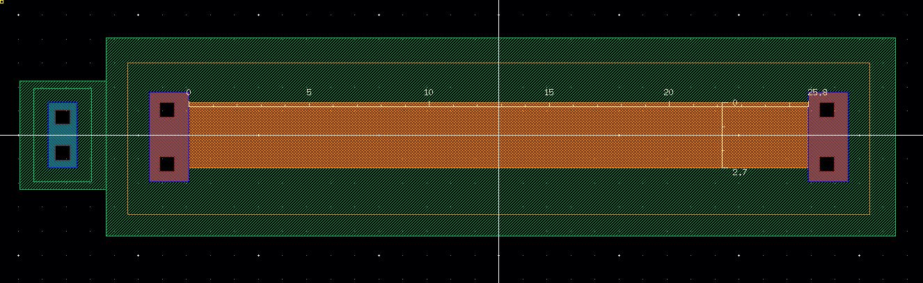
The layout of the p+ resistor is shown below.
The design directory is found in this zip file.
Return to the main Lab directory.