Lab 7 - EE 421L 

Authored by Nha Tran

Email: trann4@unlv.nevada.edu

NHSE ID: 2000590233

10/27/2014 


Lab description: The objective of this lab is to create a schematic and symbol for an 8-bit input/output array for AND, OR, NAND, XOR, and Inverter gates. Using an array of buses on one symbol makes it look more concise and professional than having a column of buses connect to the same gate.


Pre-Lab: Make a backup of the CMOSedu folder in MobaXterm by typing tar -cvf backup_oct_24_2014.tar CMOSedu/ on the command line.

ntlab7_01.PNG  


Next follow Tutorial_5 and it will show you how to connect buses and how to make a schematic and layout of a ring oscillator.

ntlab7_02.PNG

ntlab7_03.PNG


LAB:


 8-bit Inverter: first we instantiate the inverter from previous lab. then q it and change the Instance Name to IO<0:7> and set its Display to Value. Then finally we can add a thick wire by pressing shift+w and make some label like the schematic seen below.

ntlab7_04.PNG

     Next we create a symbol for our 8-bit inverter by going create CellView from CellView and delete everything except the two pins and redrawn the symbol as seen below.

ntlab7_05.PNG


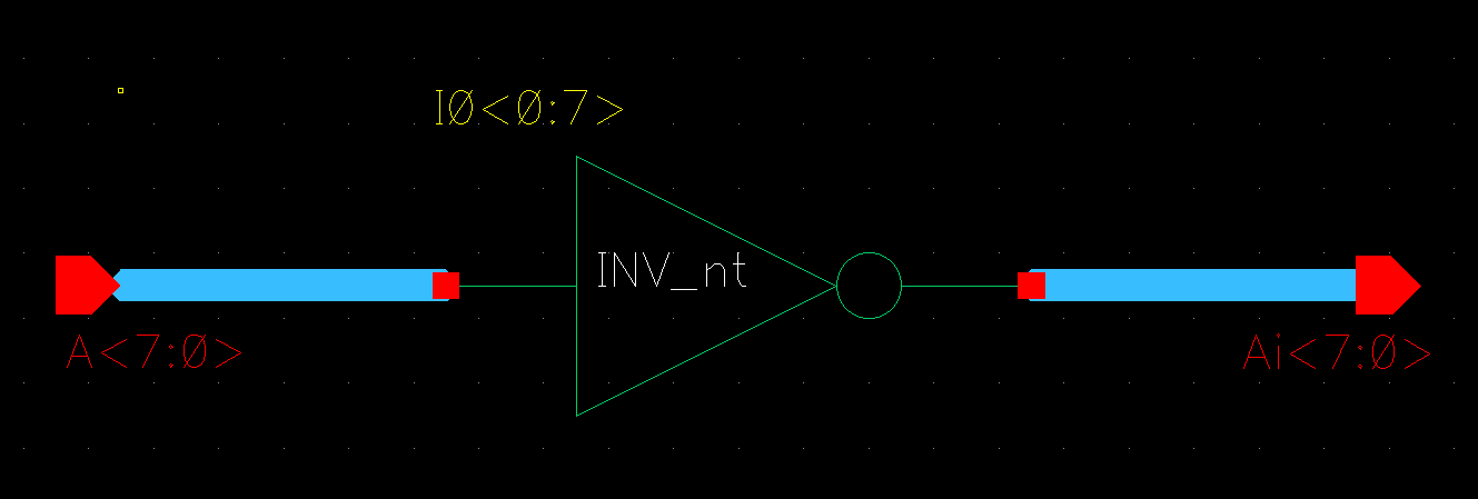
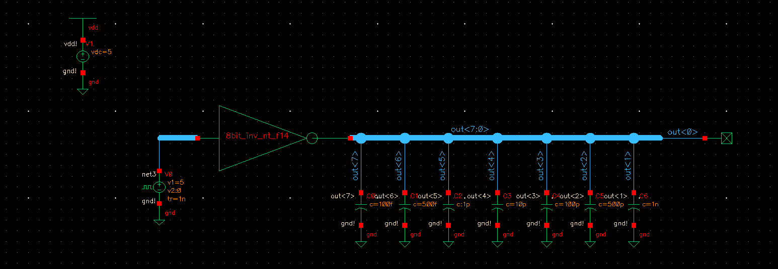
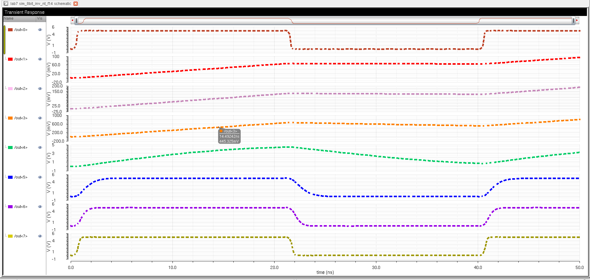
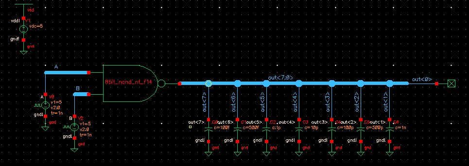
Now we will connect different values capacitor to each bit to test if our 8-bit inverter works.

ntlab7_06.PNG


notice how each output is different this is because we have different cap values so we know that our 8-bit inverter works. when you increase the capacitor you also increase the rise time and fall time. When you use td=0.7RC to estimate time delay through an RC circuit. when you increase C td willl also increases. this is the same for rise time and fall time. we use tr=2.2RC

ntlab7_07.PNG


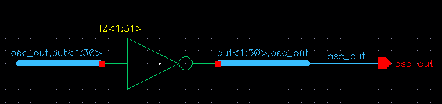
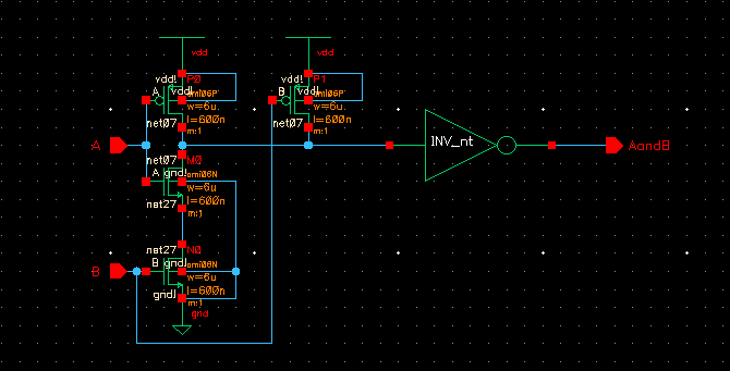
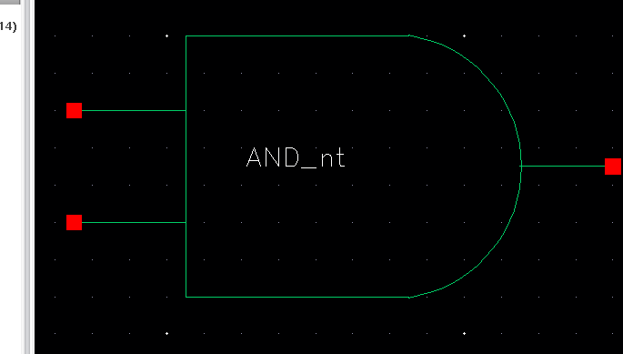
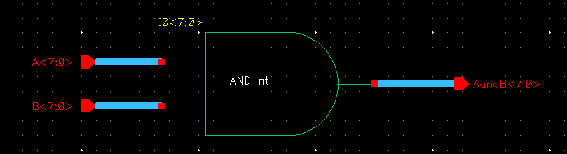
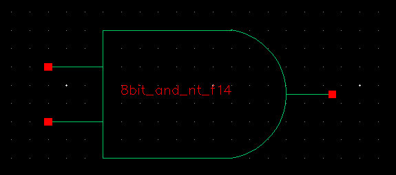
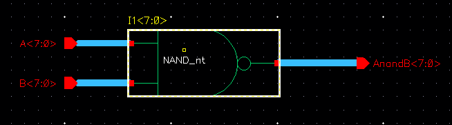
8-bit AND gate: first we make a schematic of an AND gate by putting an inverter to the output of our NAND gate. and we make a symbol of it the same way we did earlier
ntlab7_08.PNG
ntlab7_09.PNG

Next we make a bus connection to our AND symbol for the 8-bit as seen below. then we make a symbol of the 8-bit AND gate.
ntlab7_10.PNG
ntlab7_11.PNG
   
next we sim our AND gate by connecting it to a circuit like below.
ntlab7_12.PNG


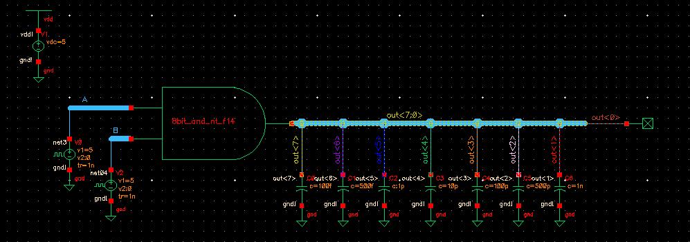
the rise time and fall time of an AND gate is affected the same way that the Inverter is.

ntlab7_13.PNG


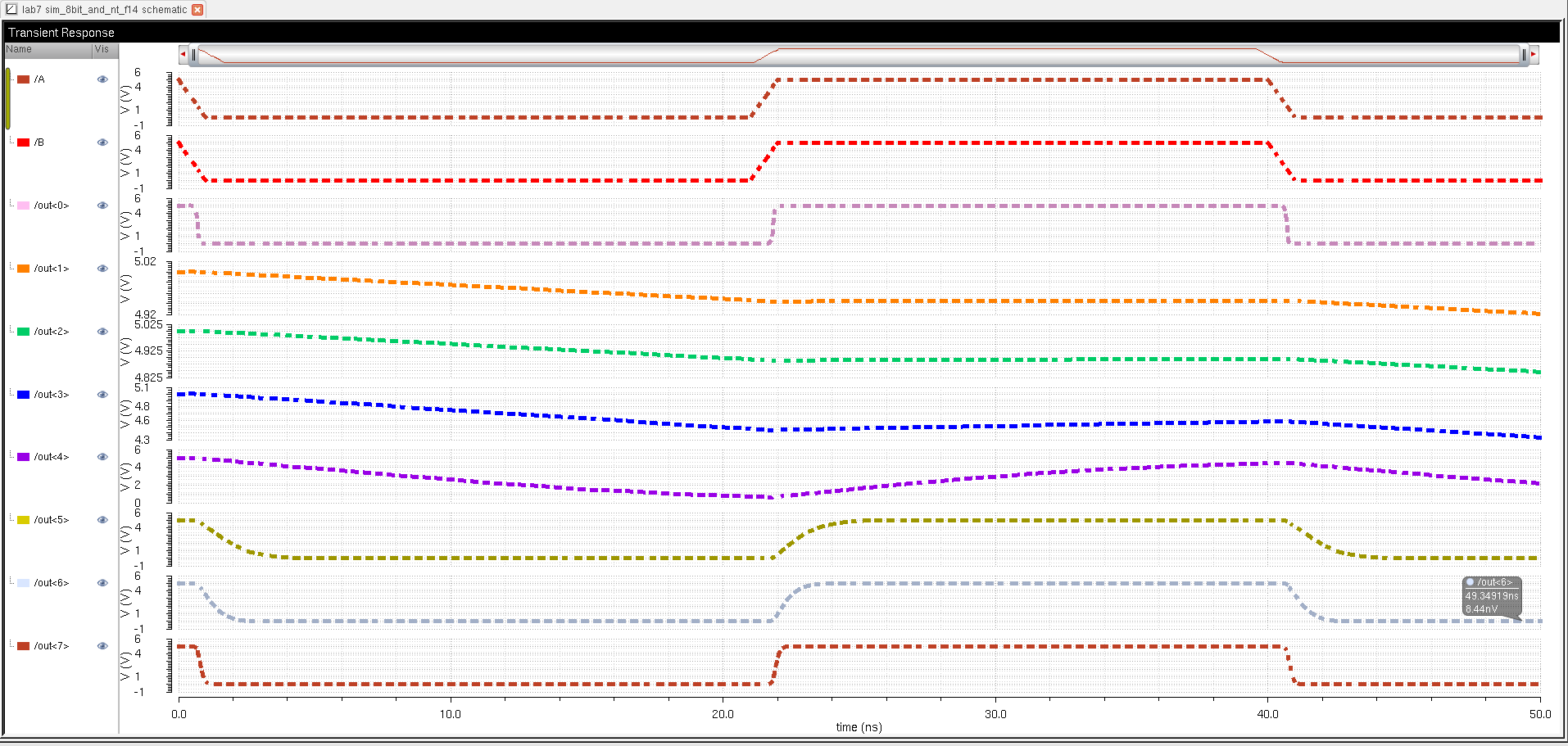
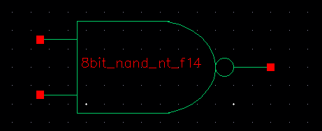
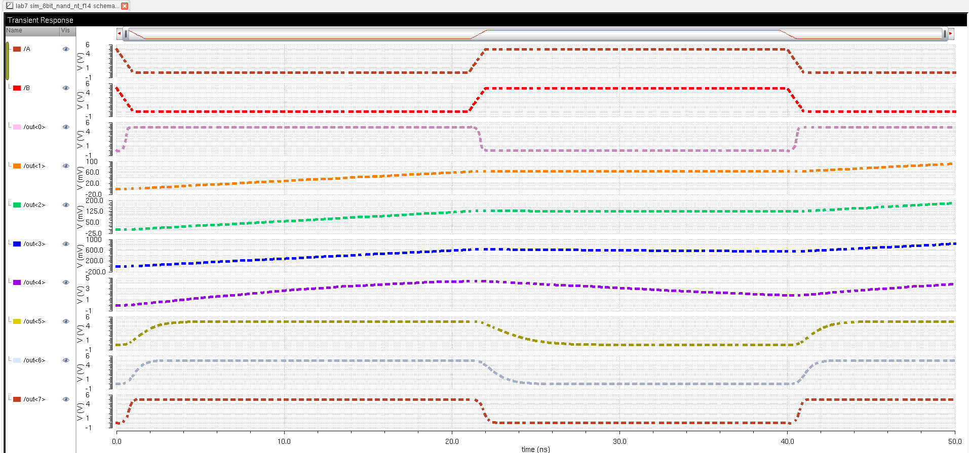
8-bit NAND gate: the NAND gate was created in previous lab so all we have to do is connect it to a bus and make a symbol of that

ntlab7_14.PNG

ntlab7_14.PNG


now we sim it just like before with the AND gate and the Inverter. 

ntlab7_16.PNG


As was predicted the same thing happens for the NAND gate also when you increase the cap the rise time and fall time also increases. Since all the gates have to same time delay and rist time equation i will forego the simulation of the last 2 gates. 

ntlab7_17.PNG


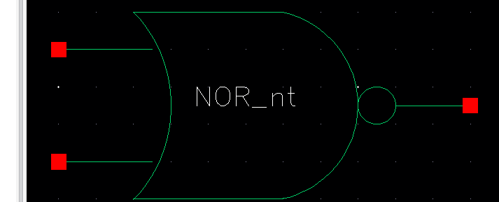
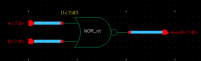
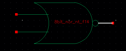
8-bit NOR Gate: first we draft the schematic of a nor gate. And also make a symbol of it similar to below.

ntlab7_18.PNG

ntlab7_19.PNG


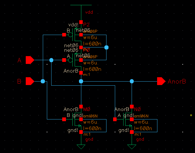
then we connect bus to like like we did in the previous gate. 

ntlab7_21.PNG

ntlab7_20.PNG


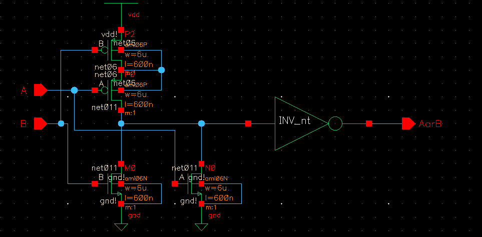
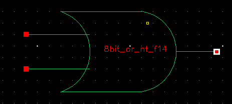
8-bit OR gate: similar to how we did the AND gate we will add an Inverter to the NOR gate to create the OR gate. 

ntlab7_22.PNG

ntlab7_23.PNG


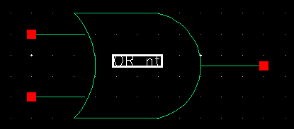
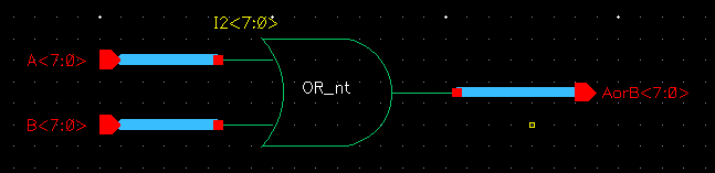
Now we create the 8-bit OR gate the same way we did for the other 8-bit gates

ntlab7_24.PNG

ntlab7_25.PNG


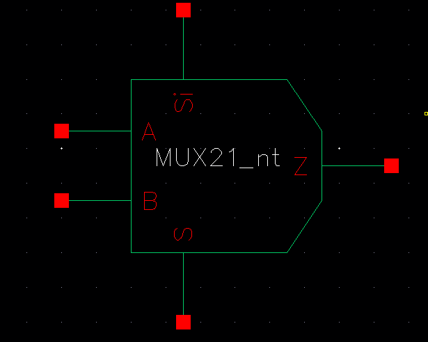
8-bit 2-1 MUX/DEMUX: first we need to draft a schematic and symbol of a single 2-1 MUX, then we will add buses to it to make it a 8-bit.

ntlab7_26.PNG

ntlab7_27.PNG

   
next we need to create a circuit like below and sim it to see the function of the MUX
ntlab7_28.PNG
   
from looking at the graph below we see that when S=1 and Si=0 the output Z =A, and when S=0, Si=1 the output Z=B. this indicate that the MUX chooses either A or B depending on the value of S. So if S=1 it chooses A, if S-0 it chooses B.
ntlab7_29.PNG


We can consider a MUX as a multiple input single output switch, and a DEMUX is a single input multiple output switch. So for DEMUX we switch our MUX schematic by 180 degree then the input would be Z and the outputs would be A,B


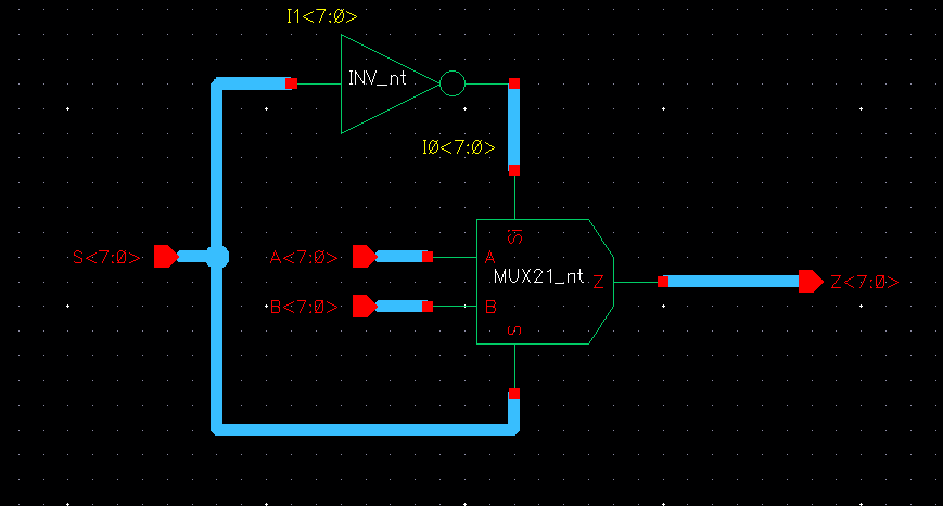
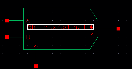
8-bit 2to1 MUX/DEMUX: for our 8-bit 2to1 MUX/DEMUX we can place an inverter connected to the S and Si. and connect the rest of the pins to buses. Then we can make a symbol for it like below. 

ntlab7_30.PNG

ntlab7_31.PNG


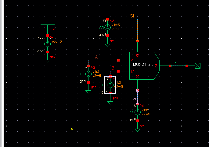
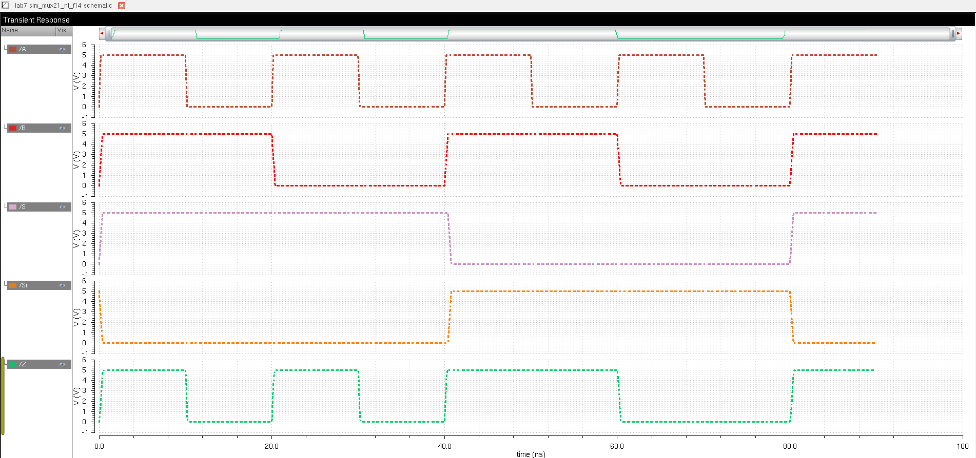
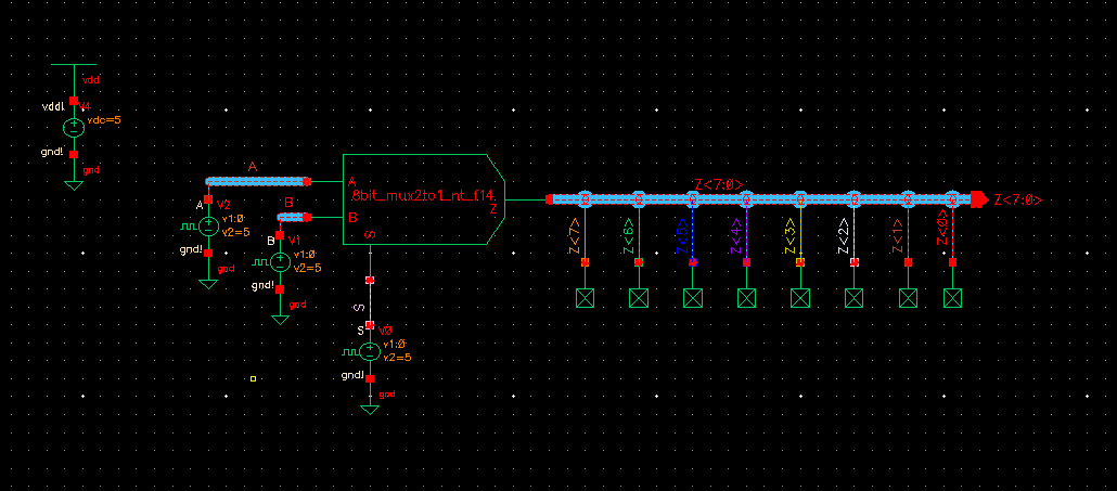
Now create a circuit similar to below so we can sim our 8bit MUX

ntlab7_33.PNG

   
Looking at the graph we see that the output for Z<0> to Z<7> matches indicating our 8-bit MUX works. and like previously discussed. when S=1 the MUX choose A, and it chooses B when S=0
ntlab7_32.PNG


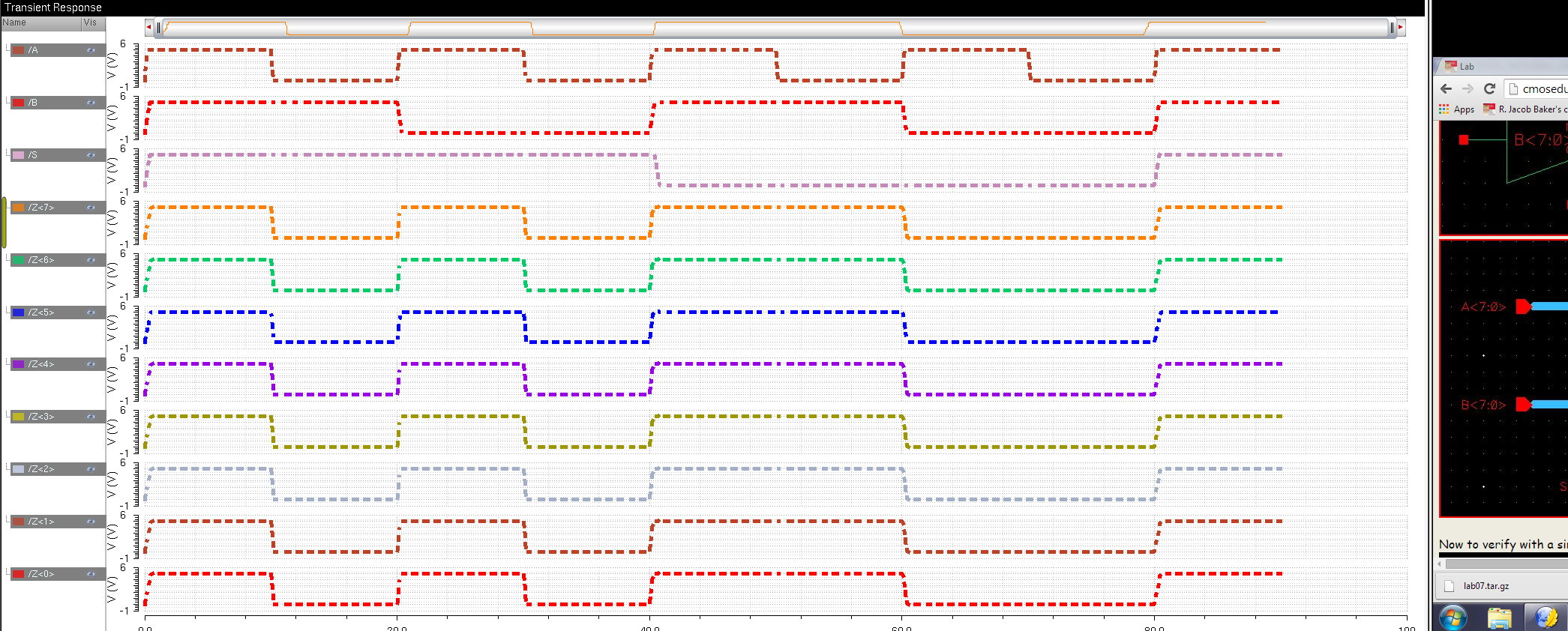
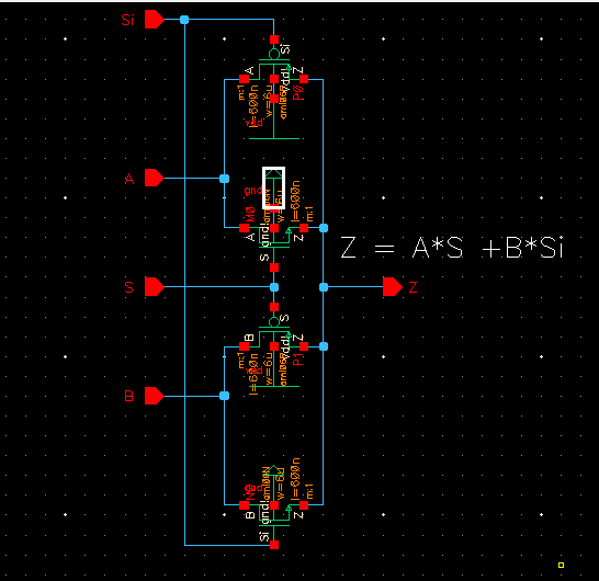
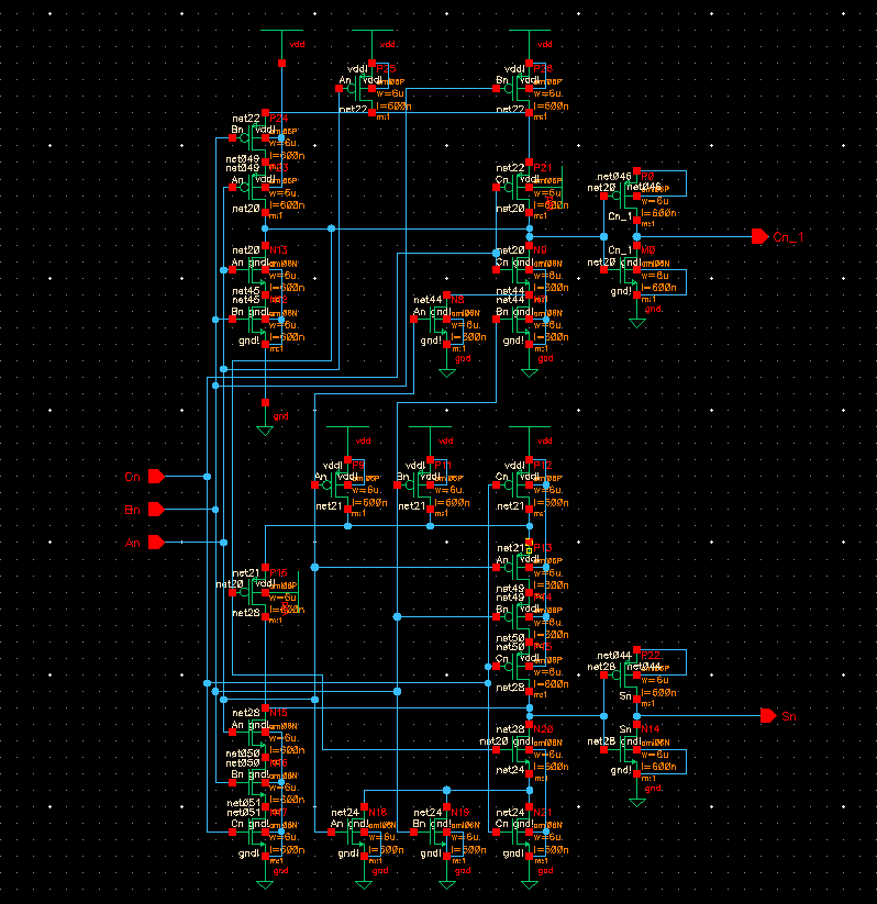
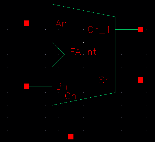
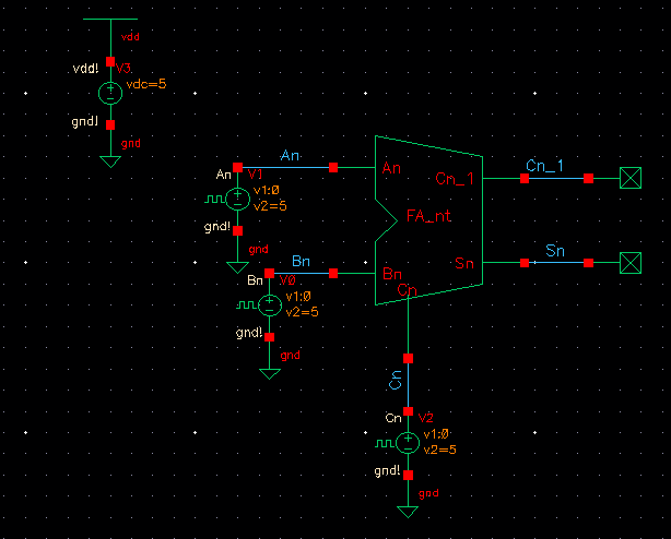
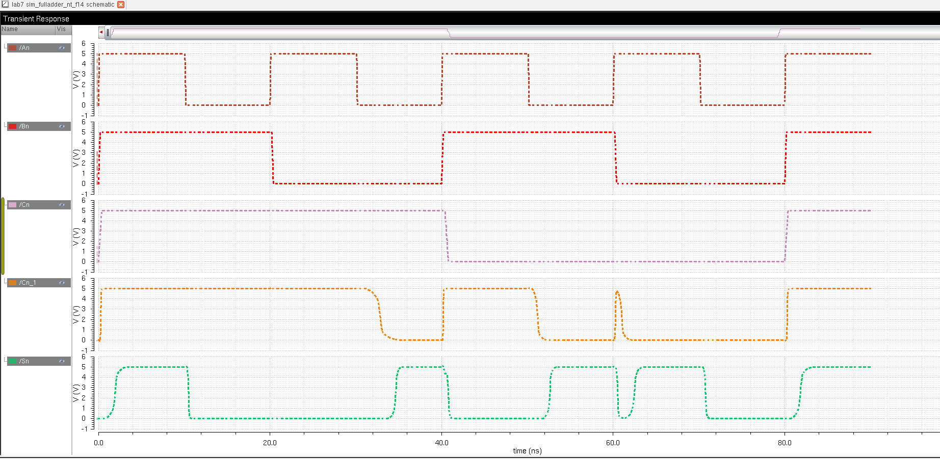
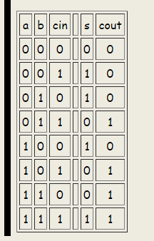
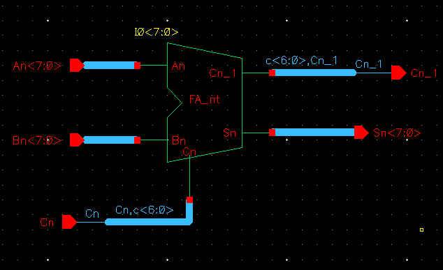
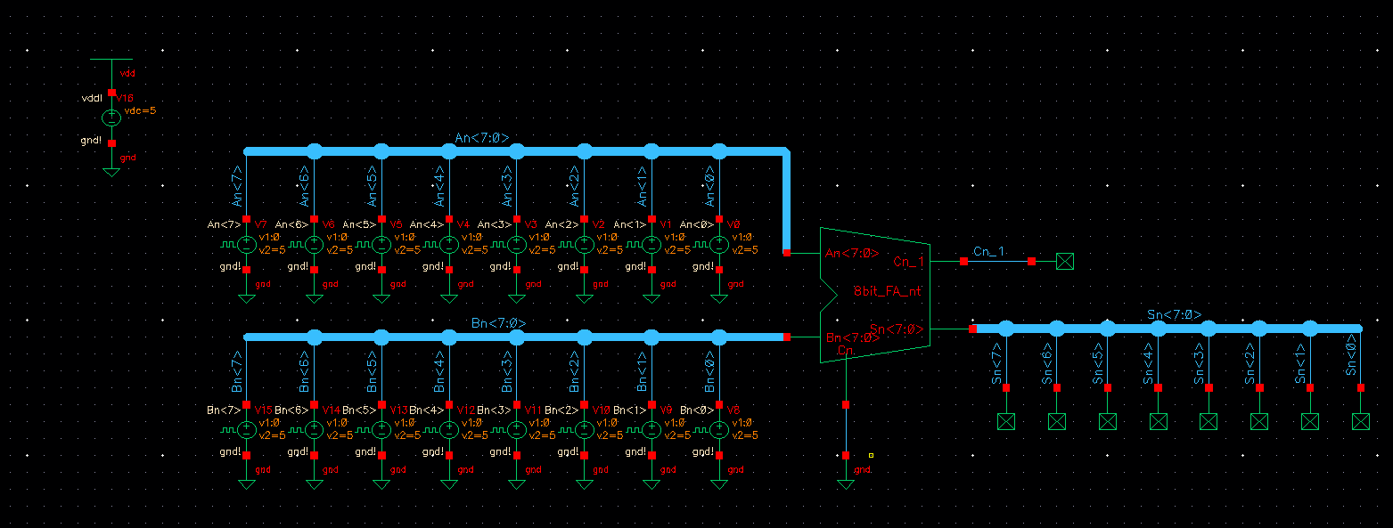
Now we create a Full-Adder as indicated on figure 12.20 on page 368 in CMOS book. first we will draft a 1-bit Full-Adder with its symbol.

ntlab7_34.PNG
ntlab7_35.PNG


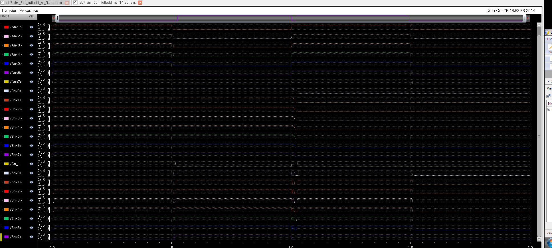
now we sim it to see if it matches our Full-Adder from previous lab. and from closer inspection of the graph it does match the truth table below of a full adder. 

ntlab7_36.PNG

ntlab7_37.PNG

ntlab7_38.PNG

     
now we are ready to make the schematic and symbol for our 8-bit Full-Adder
ntlab7_39.PNG
ntlab7_40.PNG

Now we will sim this 8-bit full-adder to see if it function correctly. because An, Bn, Cn are all 2^8 so plotting everything would take up lots of space so i choose to let Cn=0 and just plot An and Bn with the output
ntlab7_42.PNG
   
the graph is hard to tell and there are some false output cause of the gate delay but if you count individual bits it does match the truth table.
ntlab7_42.PNG


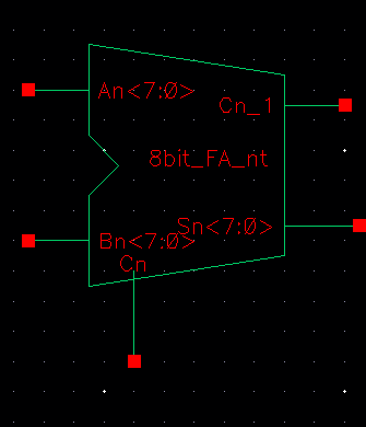
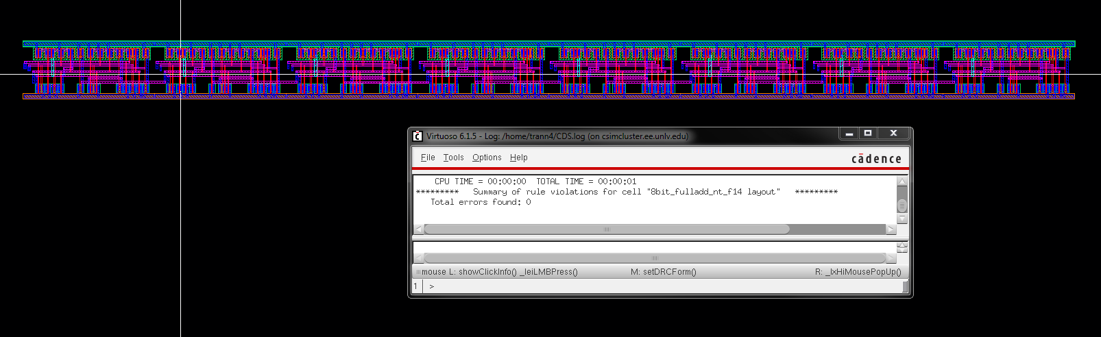
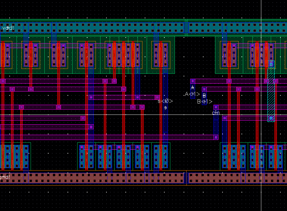
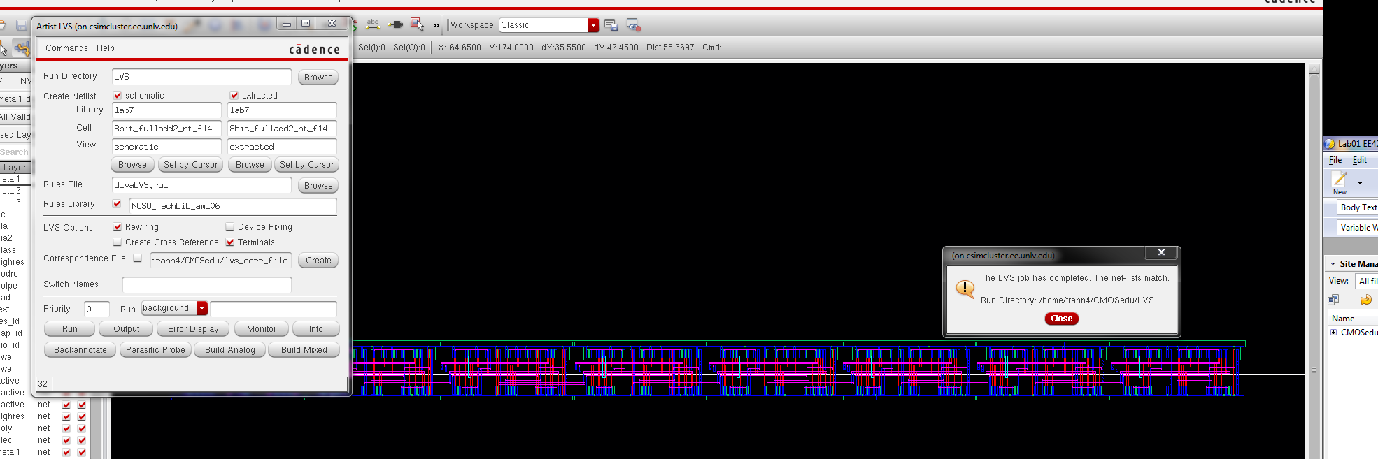
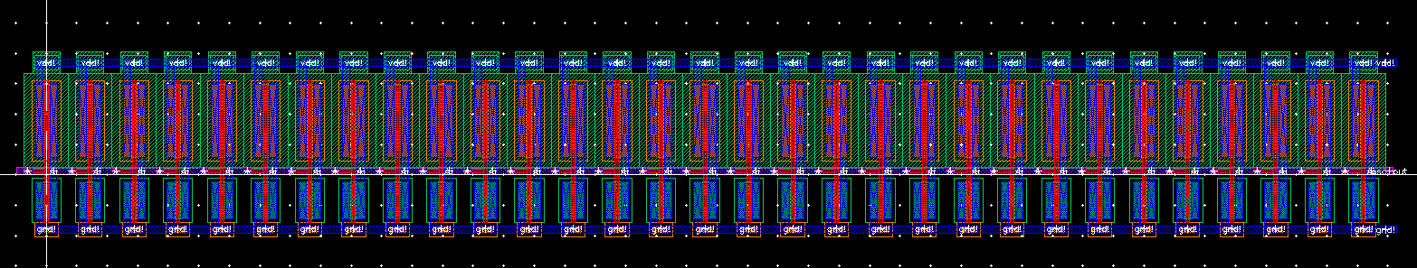
lastly i will draft the layout of the 8-bit Full-Adder. 

ntlab7_44.PNG

46.PNG
ntlab7_45.PNG

Lastly sending a copy to myself
1.PNG


lab7.zip

Return to EE 421L labs