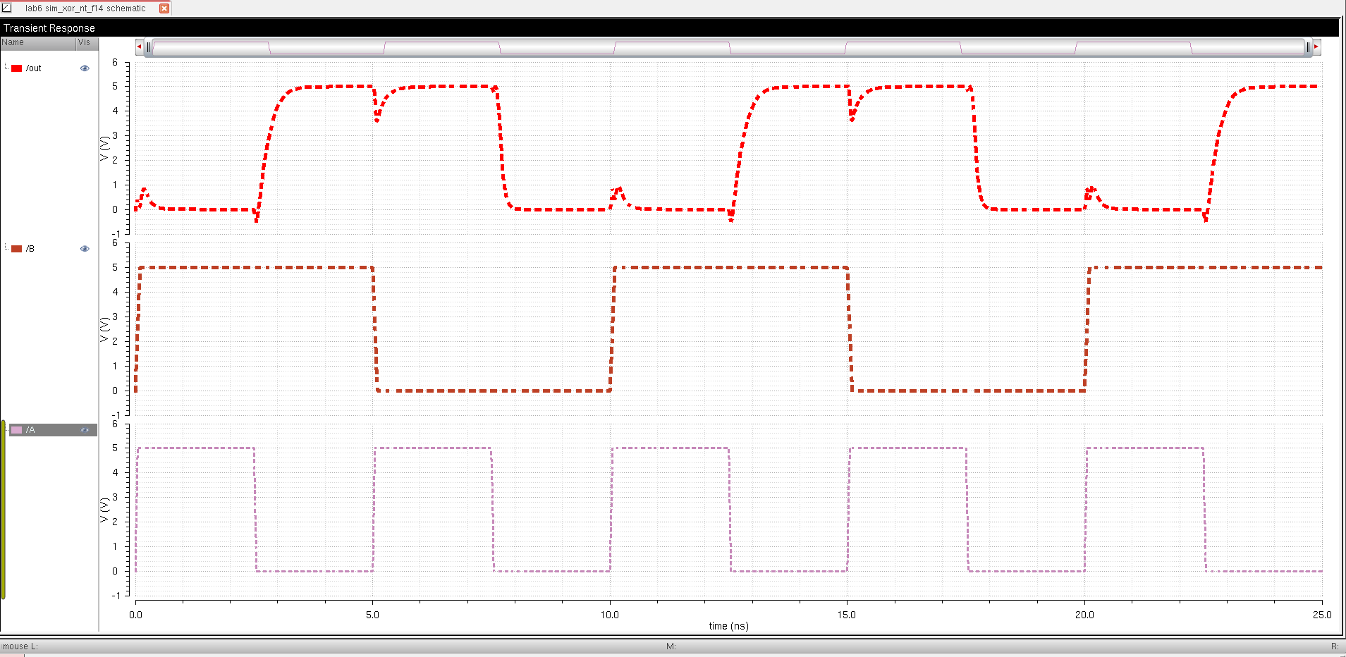
Looking at the graph we can see that when A,B = 00, 11 the output is 0, and when A,B = 01, 10 the output is 1. This indicate that our Xor gate works the way it is suppose to work. The output has moments where it is not straight this is cause by the difference in the Nmos and Pmos that is used in xor gate. the transistion where the A and B switches from 0 to 5v. there is a delay between A and B and this cause the output to not be a flat line.
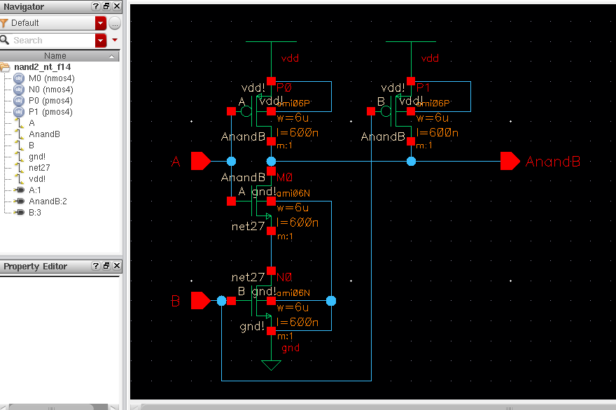
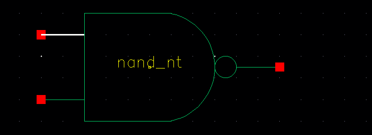
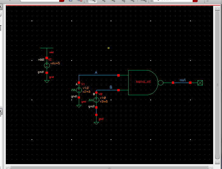
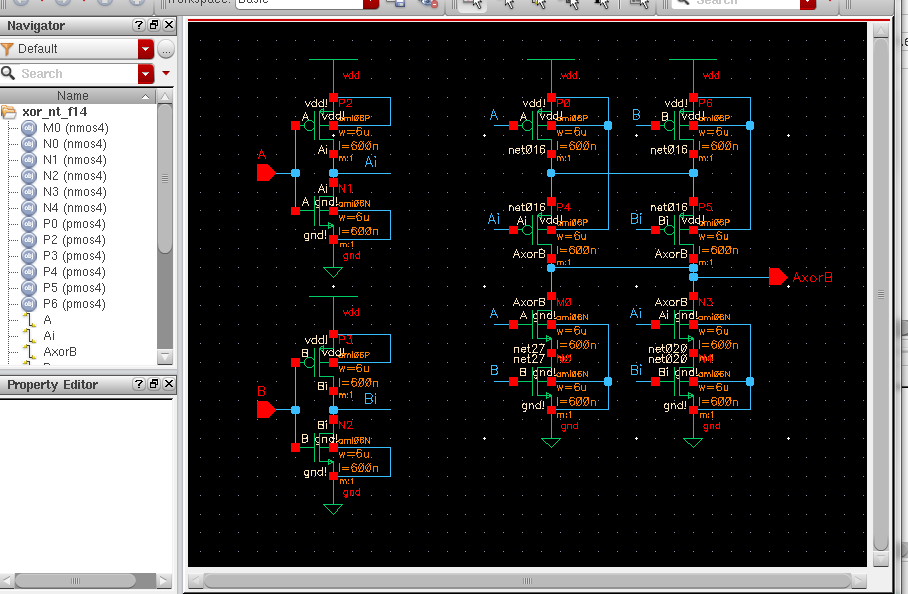
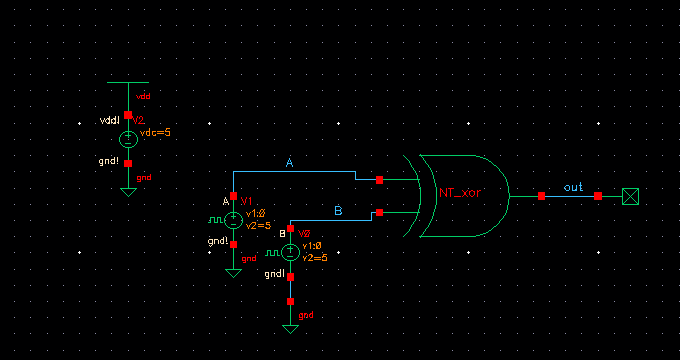
Next before we make the schematic for the full-adder, we will make a circuit that will impliment the inverter, nand, and xor gate.
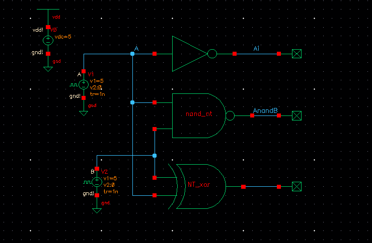
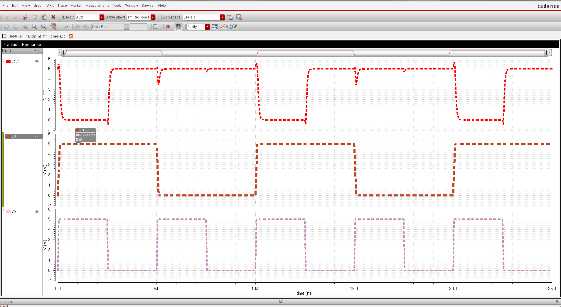
As you can see from the graph all 3 logic gates works the way it is suppose to. there is a slight delay in each of the logic gates, this is cause by the time it takes for the voltage to reach the gates. from the graph xor had a slight dip when both A and B changes simultaneously. if the period of the input were shorter this will cause an error in the reading because that dip would look like it have a false output. Other than that everything is working fine. however if our circuit contain multiple gates that goes to the same output and the gates for A and B is not equal when we reach the output, than it will cause the same delay problem. Because the xor gate is bigger in size compared to the nand gate it would be logically to think that there is a bigger time delay to reach the output in the xor gate than the nand gate.
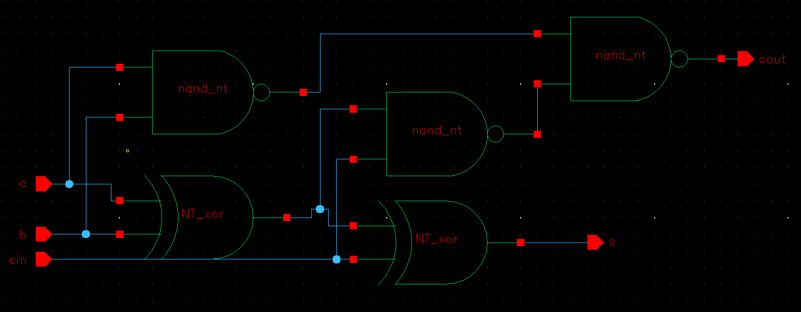
Next we will draft the schematic for a full-adder by connecting our nand and xor gate like below.
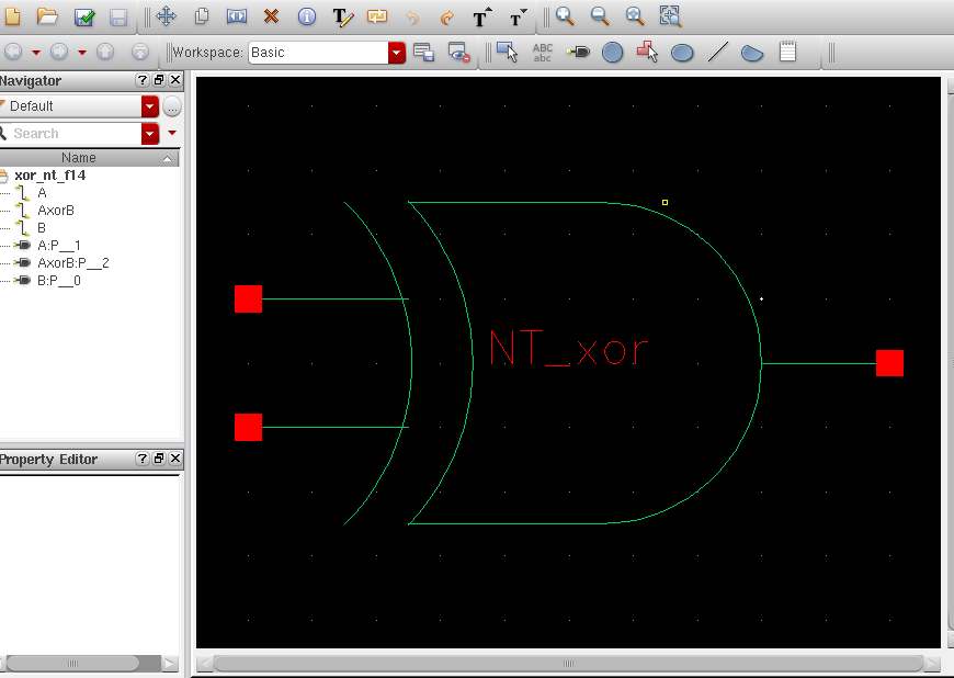
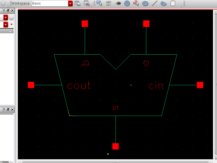
Next we create a symbol for the full-adder like below.
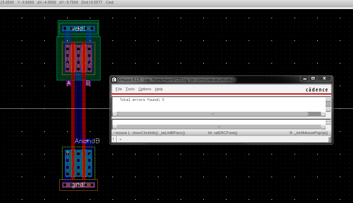
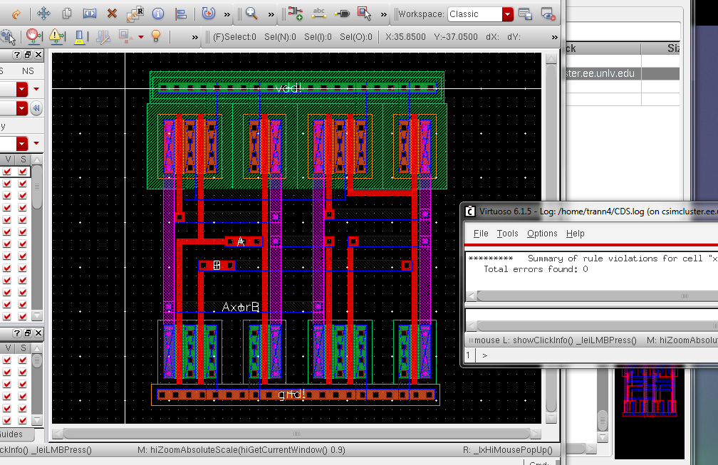
Next create a layout of the full-adder like below. then DRC it and make sure it have no error.
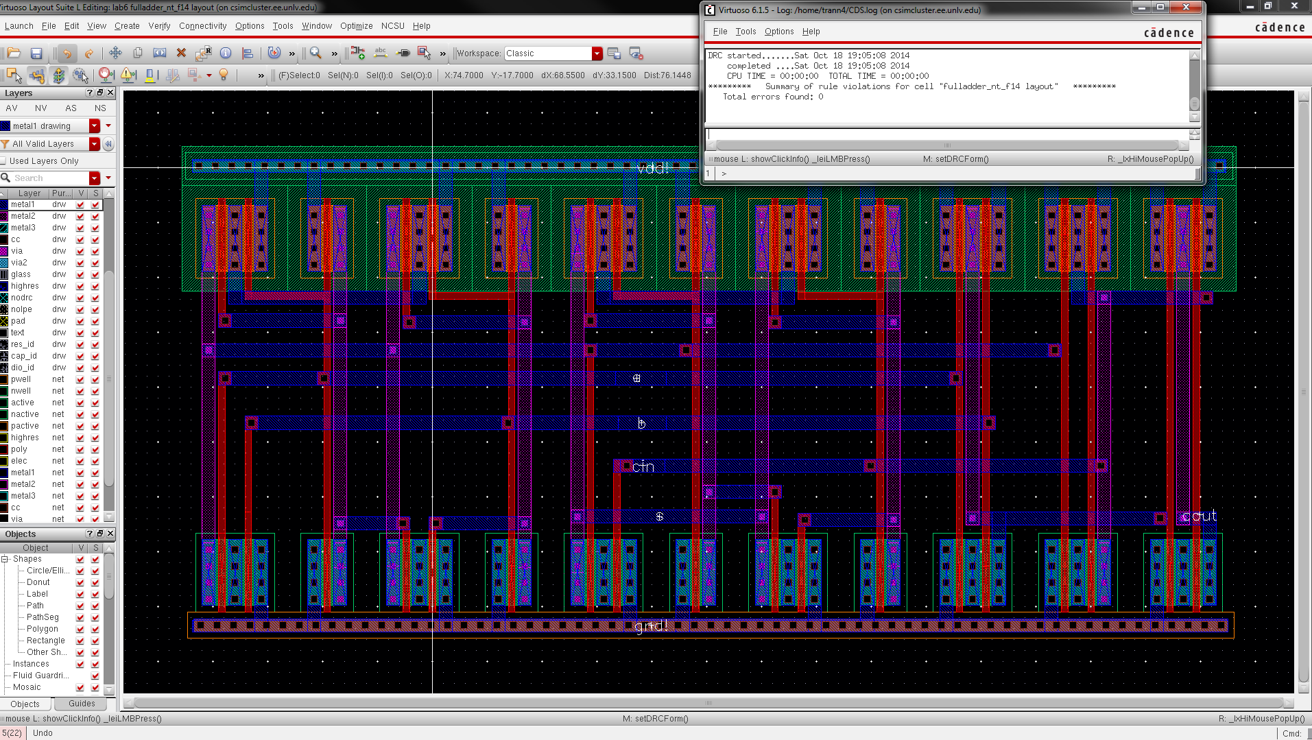
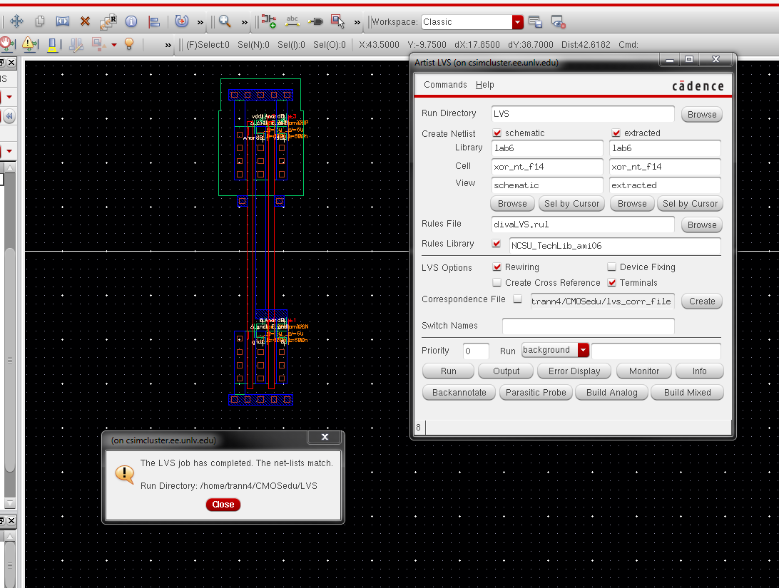
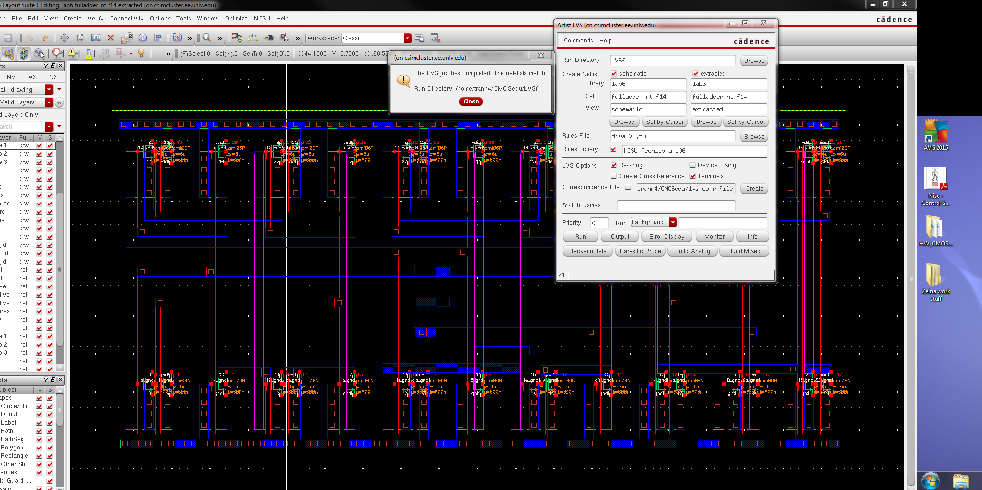
next extract the layout and LVS it with the schematic to make sure they match.
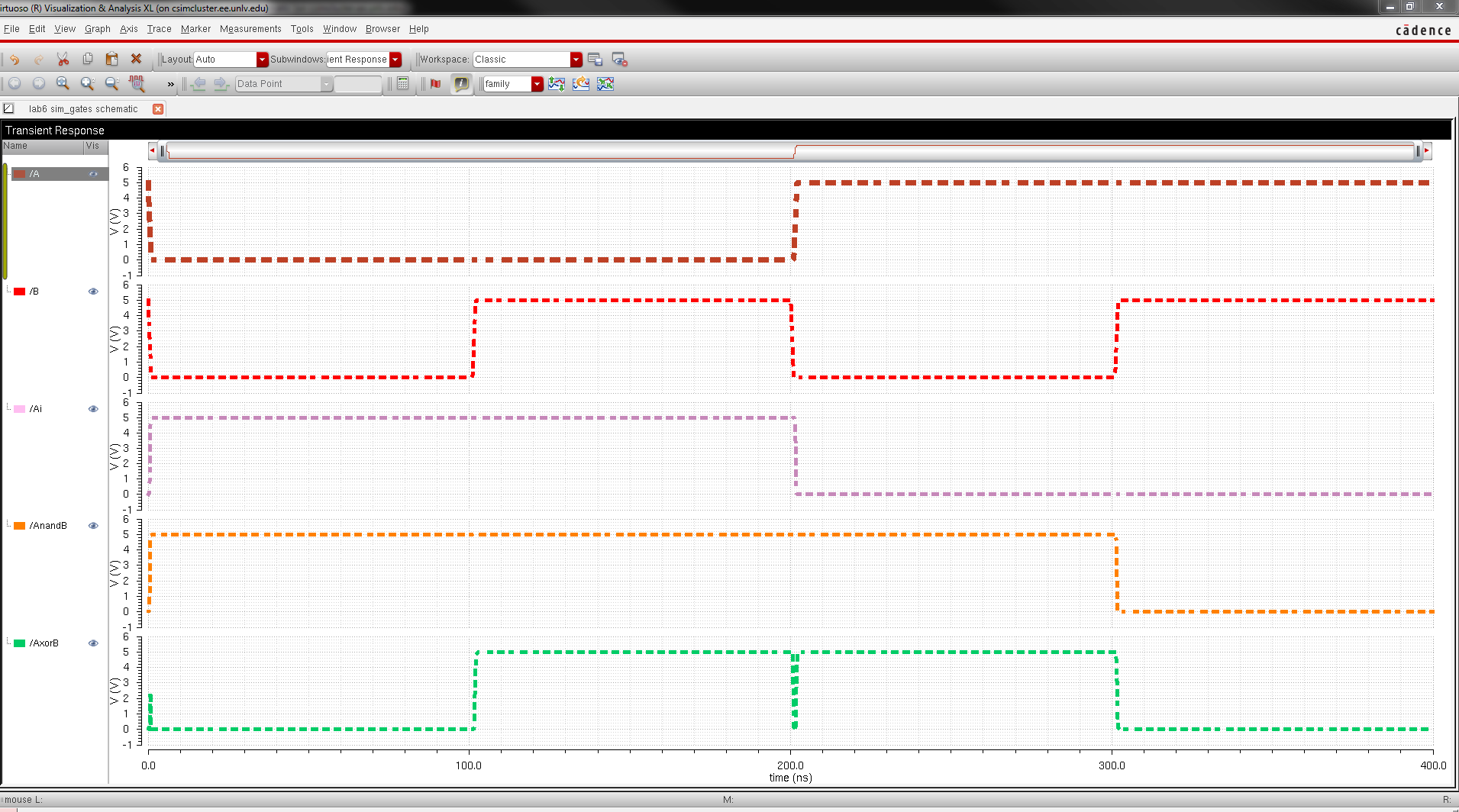
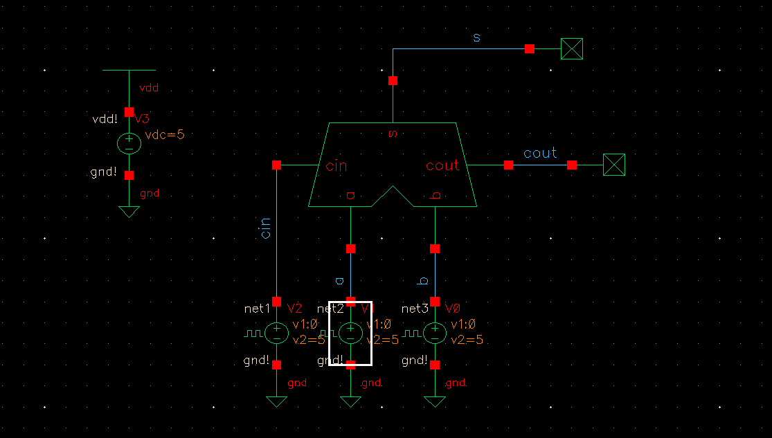
lastly draft the schematic as shown below to simulate the full adder.
Cin, A, and B should be an 8-bit input while S and Cout should be the output. the following table shows how the graph should be if it matches.
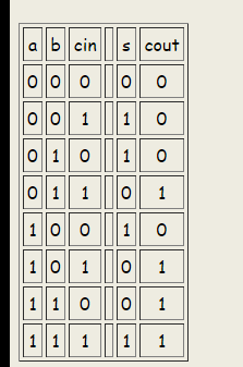
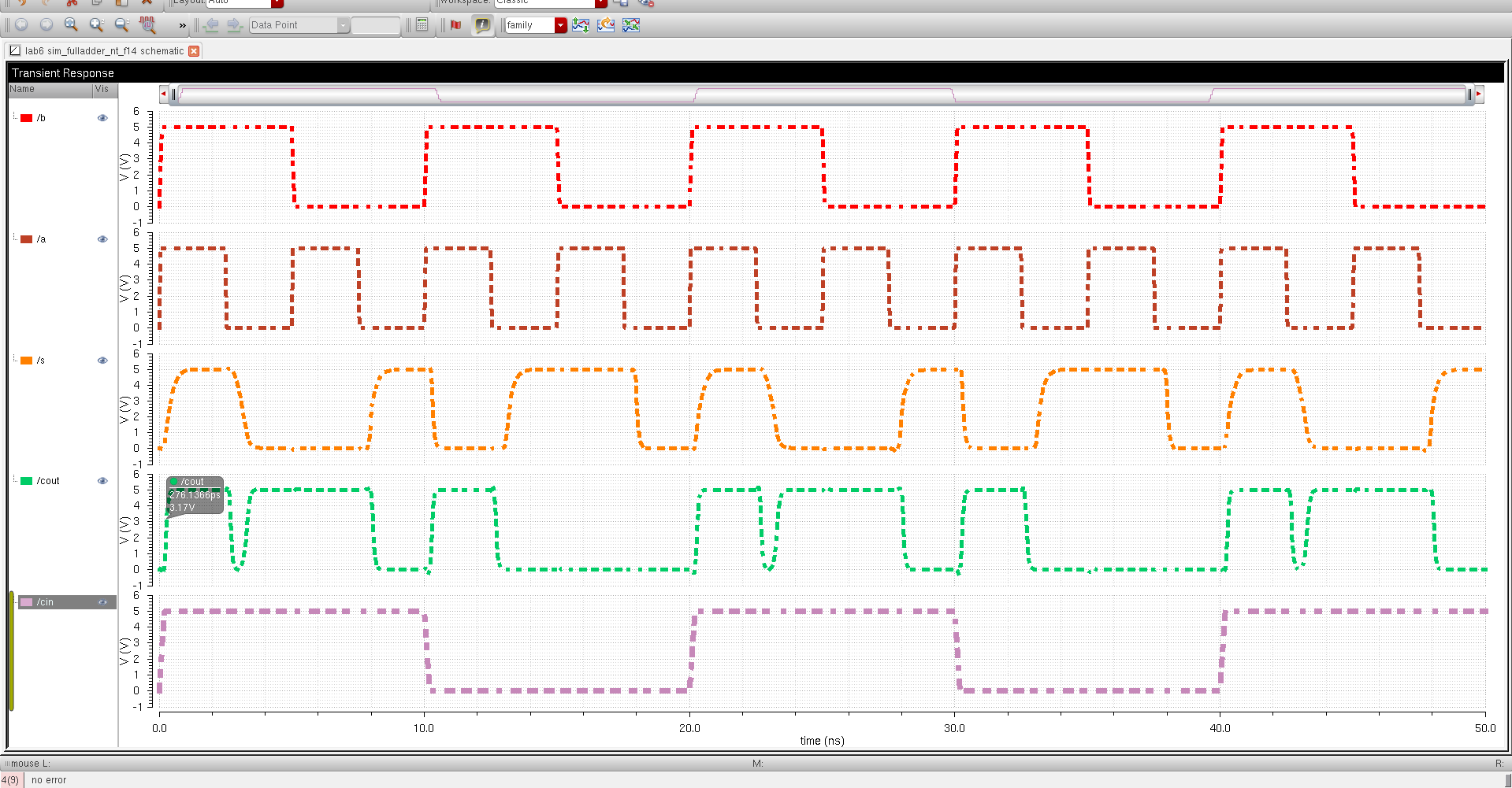
As you can see the graph matches the truth table. when A,B and Cin = 111, the Cout and S =1, when A,B, Cin = 110, Cout is 1 while S =0, along with all the other input from 000 to 111 the output matches the truth table indicating that our full-adder works.
lastly zip up everything and email to self.

link to lab6.zip folder where the schematic, layout, and symbol are located