Lab 5 - EE 421L
Authored
by Nha Tran
Email: trann4@unlv.nevada.edu
NHSE ID: 2000590233
10/13/2014
Lab
description: The purpose of this lab is to draft a layout, schematic and symbol of an inverter.
Prelab:
First zip up the cmosedu folder by typing tar -cvf
1. What does the Bindkey q do?
properties
2. Which two Cell Views are
used when doing an LVS?
schematic and extracted
3. What is the difference
between the nmos and nmos4 schematic cells?
one has 4 pin and one has 3
4. How do you select the
MOSFET models in the ADE window? What does ADE stand for?
go to model
library and find it in the ami06 folder, ADE is analog design
environment
5. What is the difference
between moving and stretching?
one move and one stretches
6. How do you layout a
rectangle on the metal1 layer?
press R then draw a rectangle
7. What does the ! indicate
at the end of gnd! and vdd!
it means universal or global
8. What do the acronyms LSW
and CIW stand for?
LSW - layout
selection window, CIW - command interpretor window
9. How is the ruler used?
Cleared?
press k, shift k to get rid of it
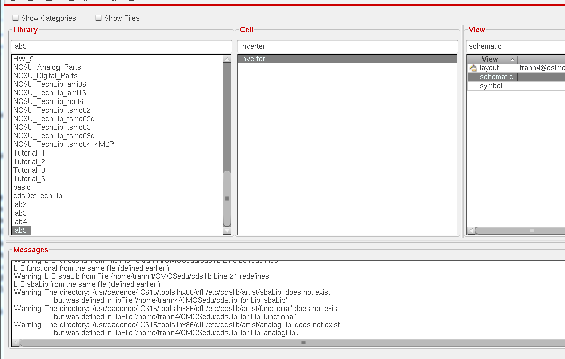
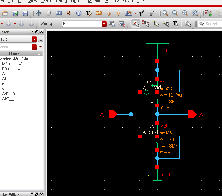
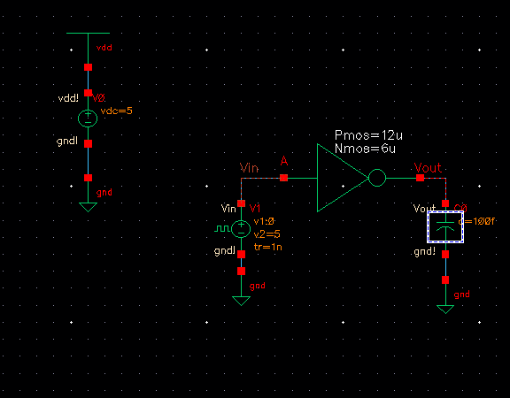
Create a new library name it lab5 and create a new cell view in that folder and name it inverter.
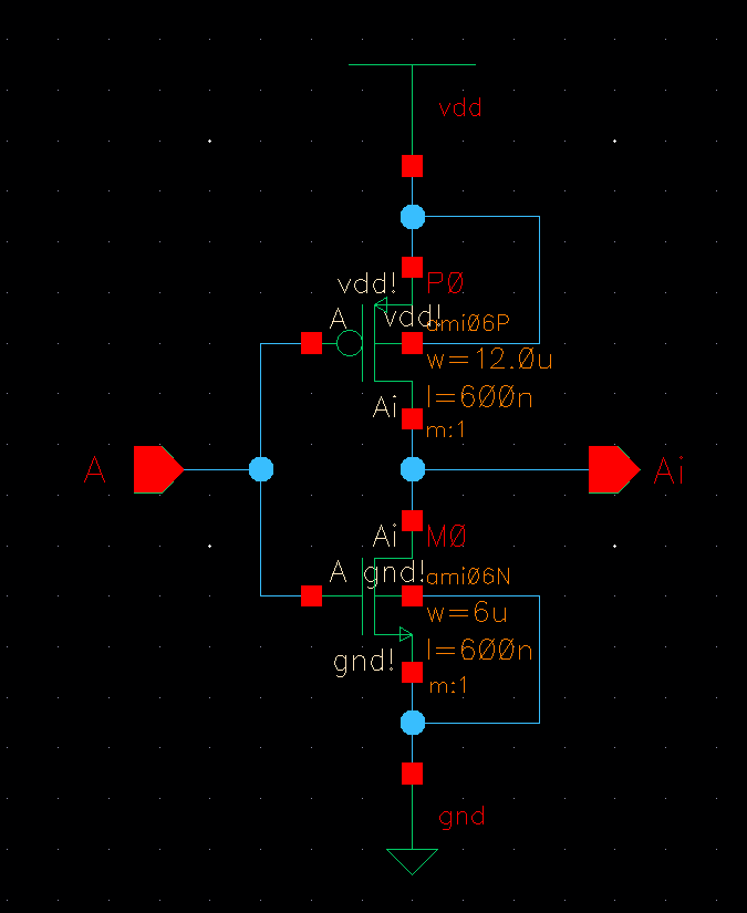
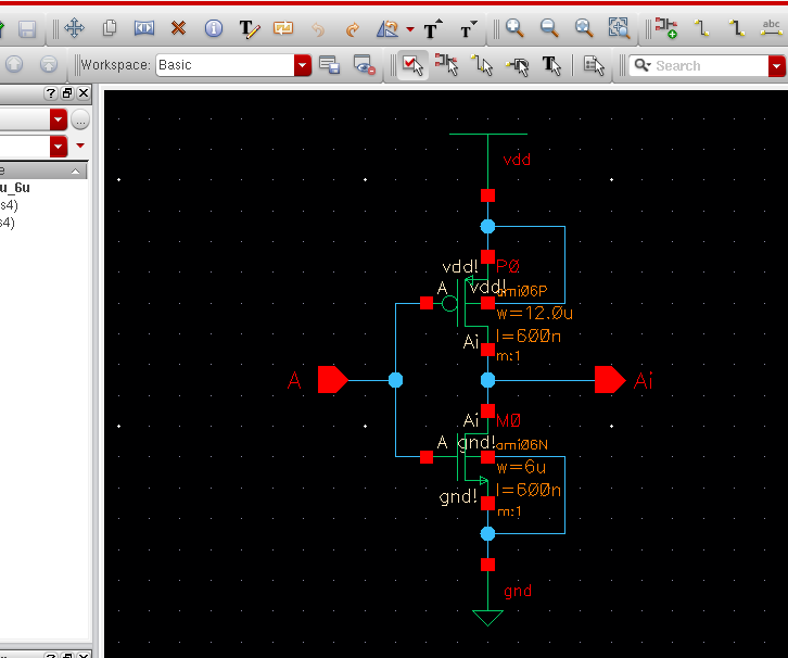
get
the NMOS and PMOS from the NMOS_IV and PMOS_IV schematic and add the
vdd and gnd to the pmos and nmos respectively. also add an Input pin
lable it A and output pin label it Ai. and connect wires to make the
schematic similar to below.
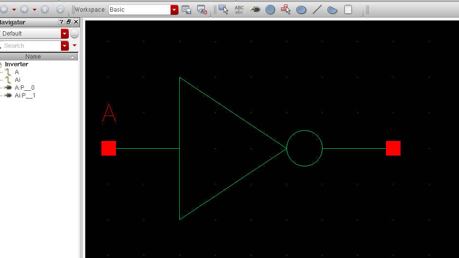
save the schematic and create the cell view from cell view. Then delele everything and redraw the inverter like below.
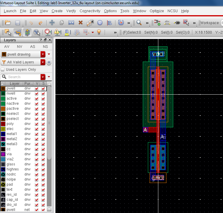
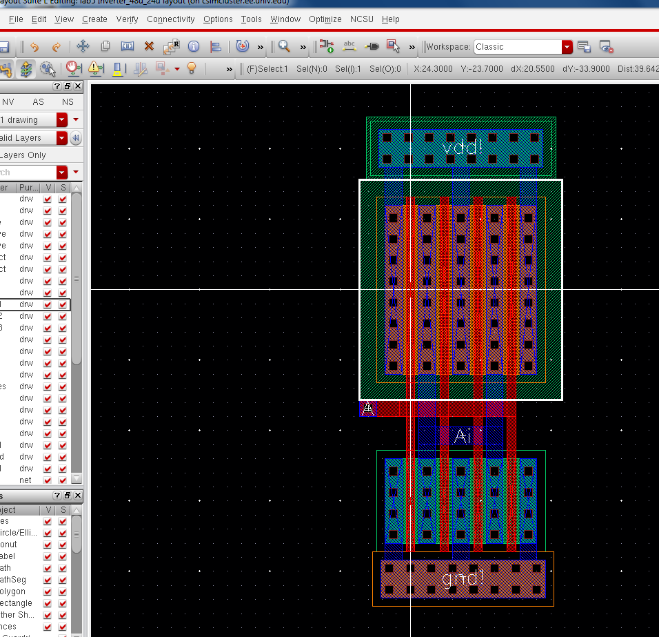
next create new layout for the inverter, and instantiate the following instance from the ami06 library.
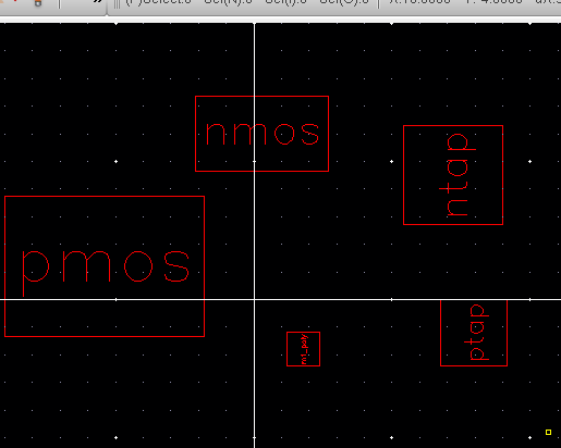
next
align the layout like below, and make the pmos 12u by 600n and the nmos
6u by 600n, make the ntap and ptap have 2 column of contact. DRC and it
has zero error.
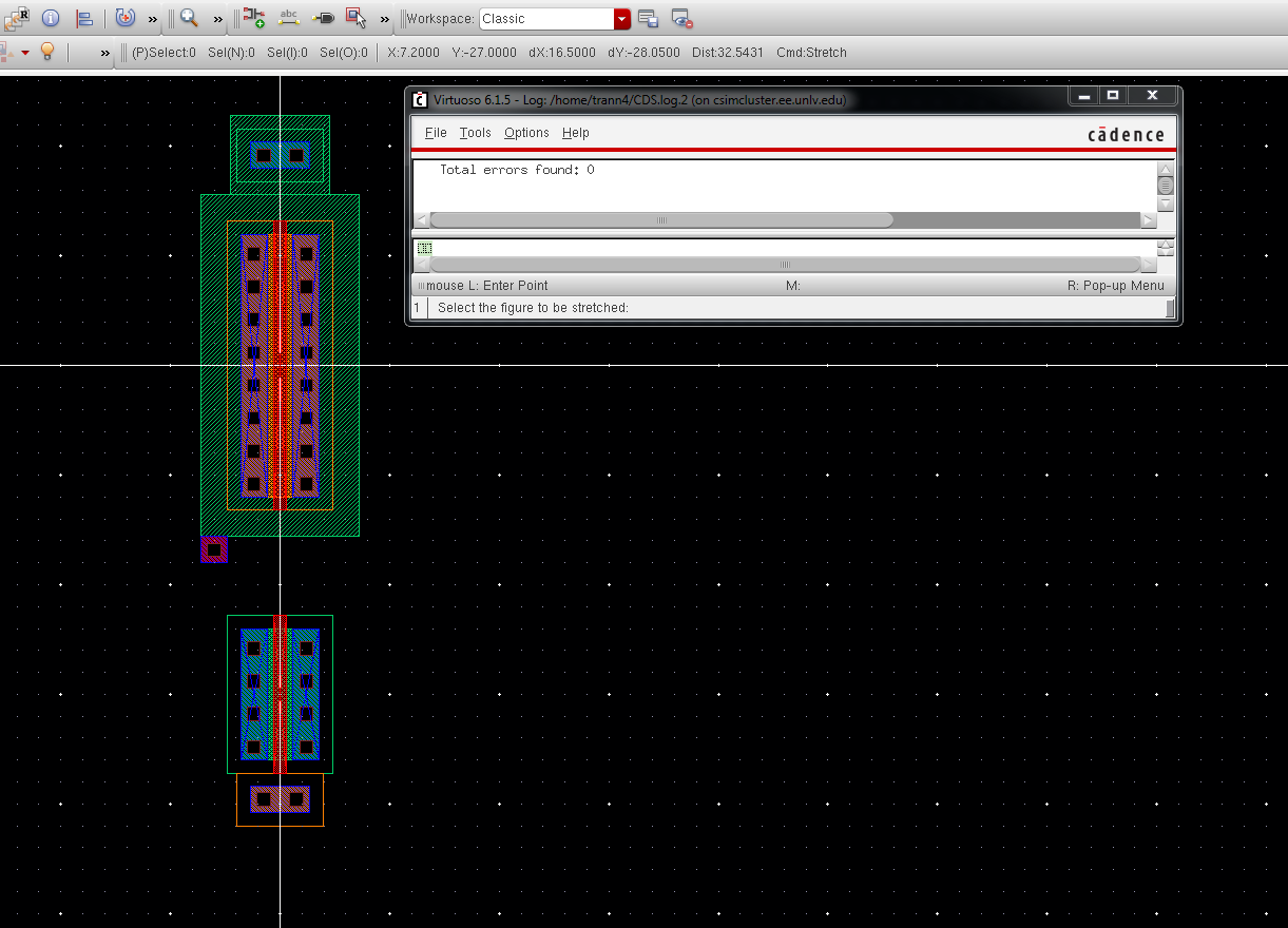
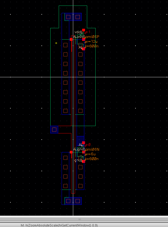
next add the metal1 and poly layer like below, DRC it and it gets zero error
when you press e and set the stop = 0 you should get the following image, with the metal1 layer connect to the layout as follow
next
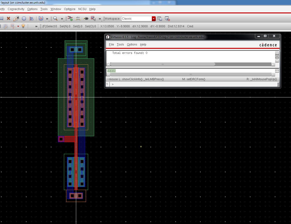
add the pin vdd! and gnd! to the ntap and ptap respectively and add the
input A and output Ai to the layout. DRC shows no error
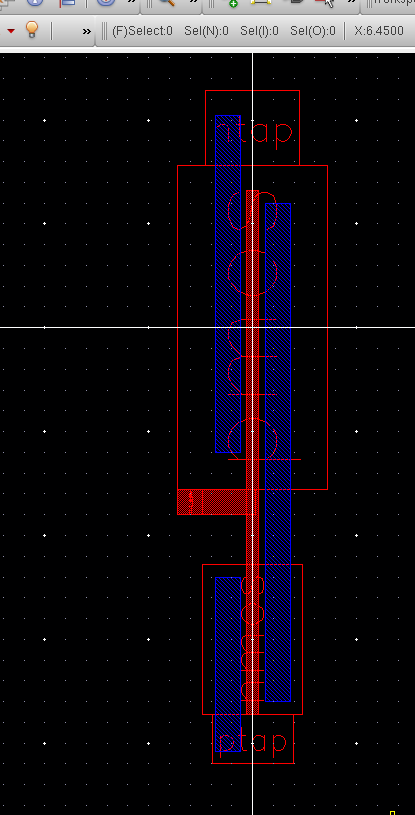
extracting the layout and it should look like below.
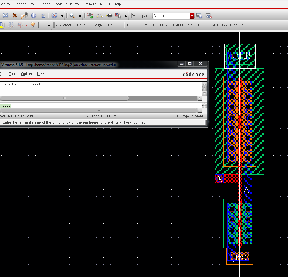
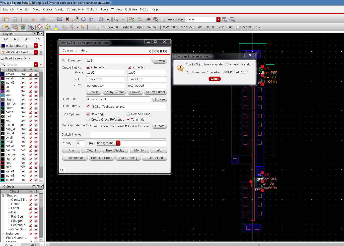
now
we will LVS the schematic with the extracted. as seen below it matches
indicated that our layout is exactly like our schematic of the
inverter.
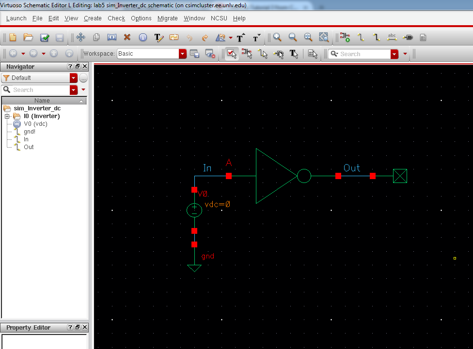
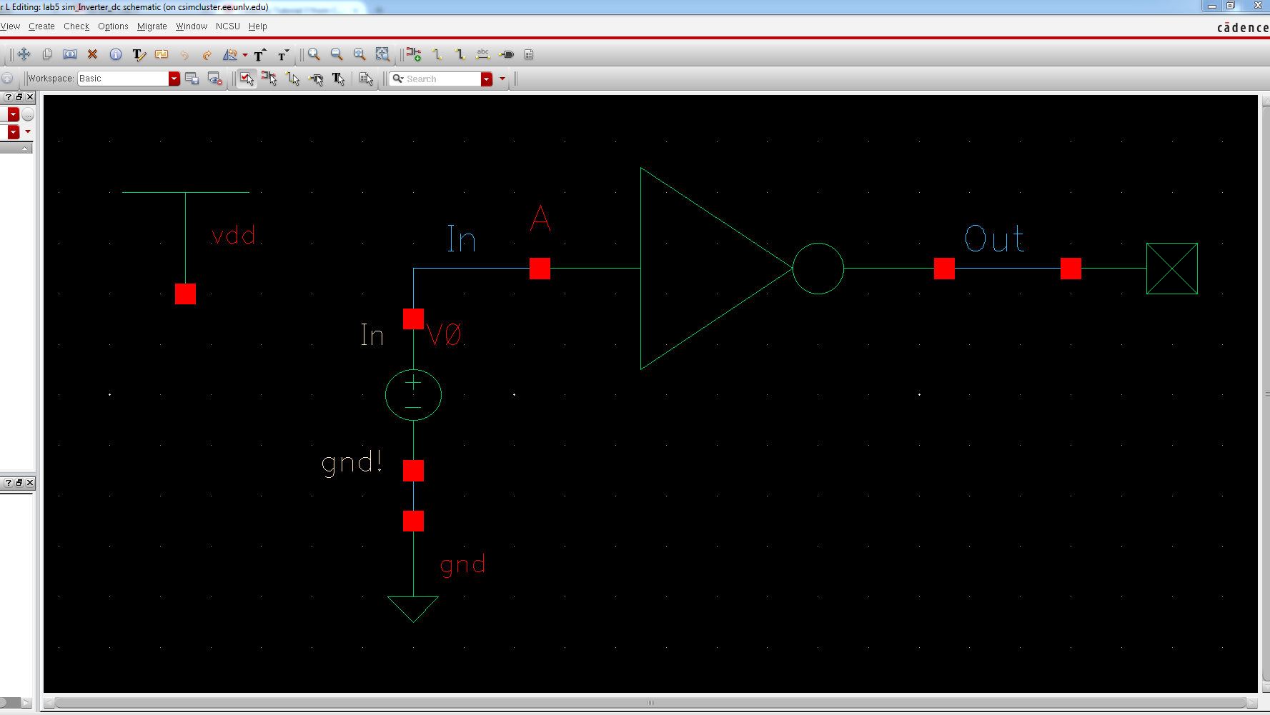
next
create a new schematic name is sim_Inverter_dc, instantiate the
inverter, and the no connection symbol in the basic --> misc
library. adding the label in and out to the schematic like below.
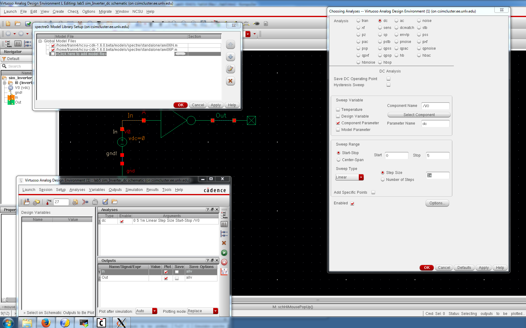
run
ADE L, then select the input and output on the schematic to be plotted.
then select dc analysis and choose the following parameter like below.
and go to model libraries and go to the ami06N and ami06P like below.
save the session and netlist and run and you should see the graph similar to below. the output is zero because there is no vdd.
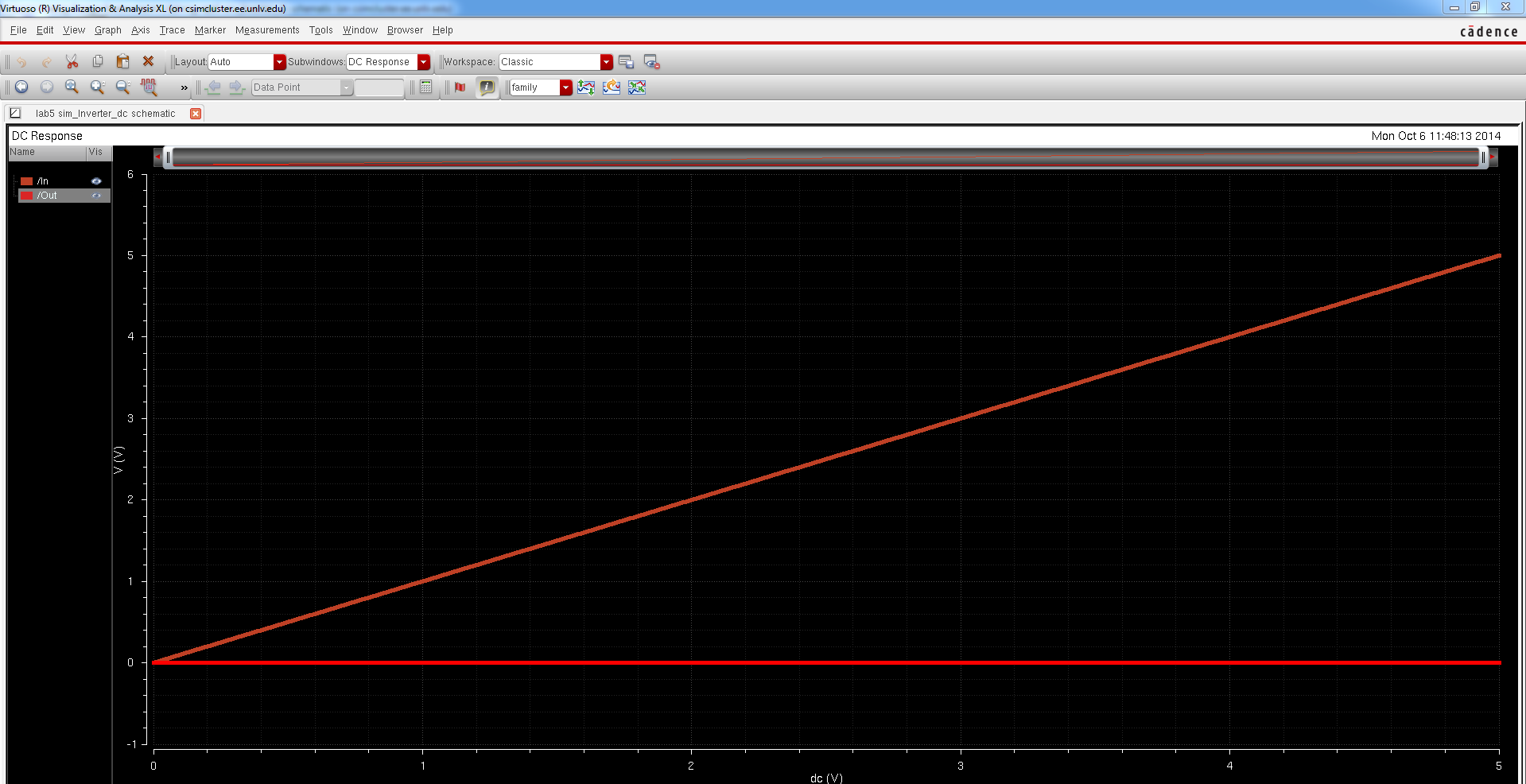
now add a vdd to our schematic.
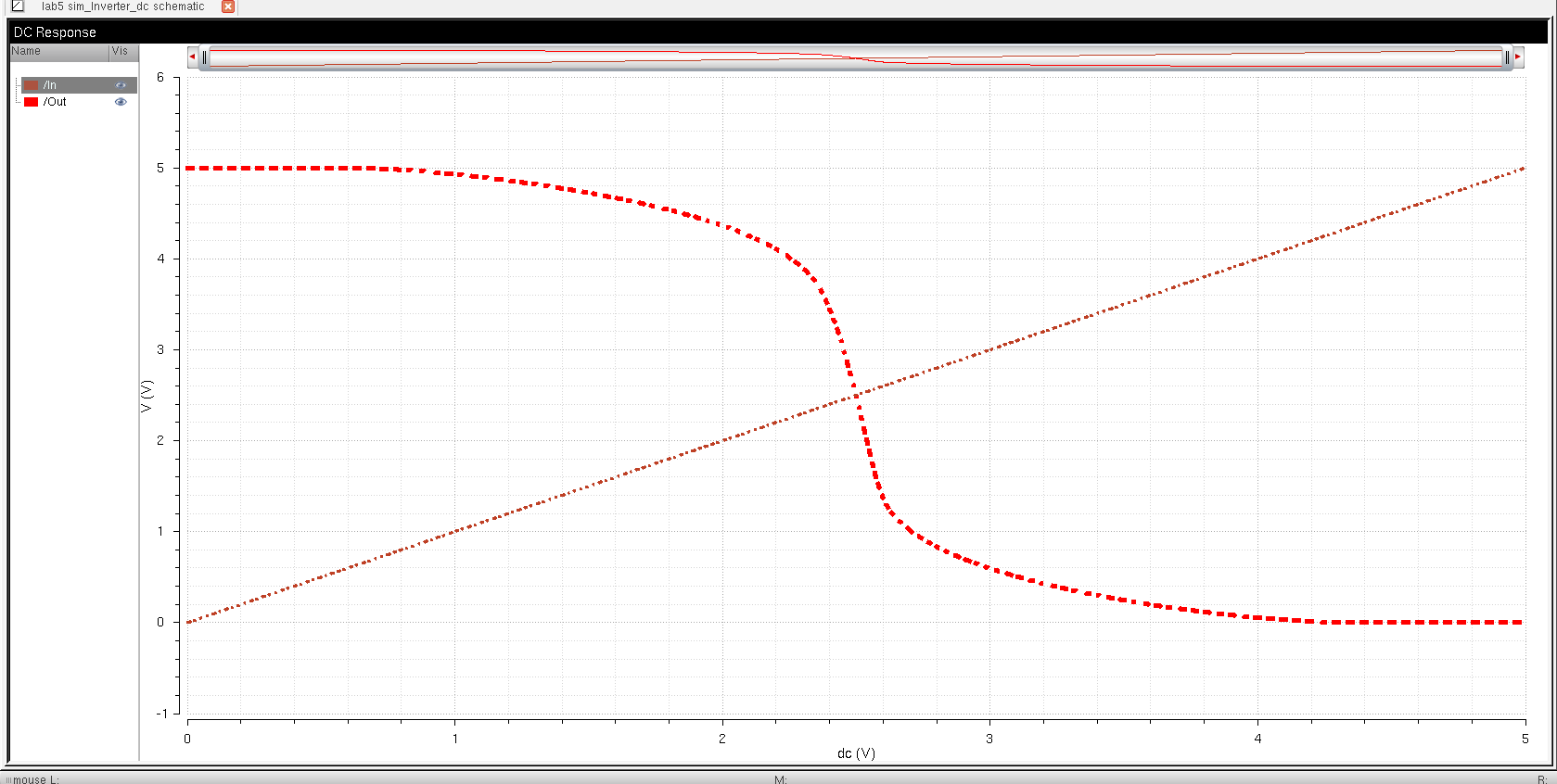
Netlist and Run you should get
End of Prelab.
LAB:
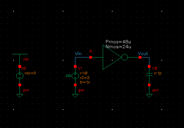
- Draft schematics,
layouts, and symbols for two inverters having sizes of:
- 12u/6u (= width of the
PMOS / width of the NMOS with both devices having minimum lengths of 0.6u)
- 48u/24u where the devices use a multiplier, M = 4 (set along with the width and length of the MOSFET), as seen below
schematic of a 12u by 600n Pmos and 6u by 600n Nmos.
| schematic of a 48u by 600n Pmos and 24u by 600n Nmos. |
 |  |
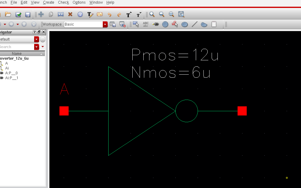
symbol of a 12u by 600n Pmos and 6u by 600n Nmos.
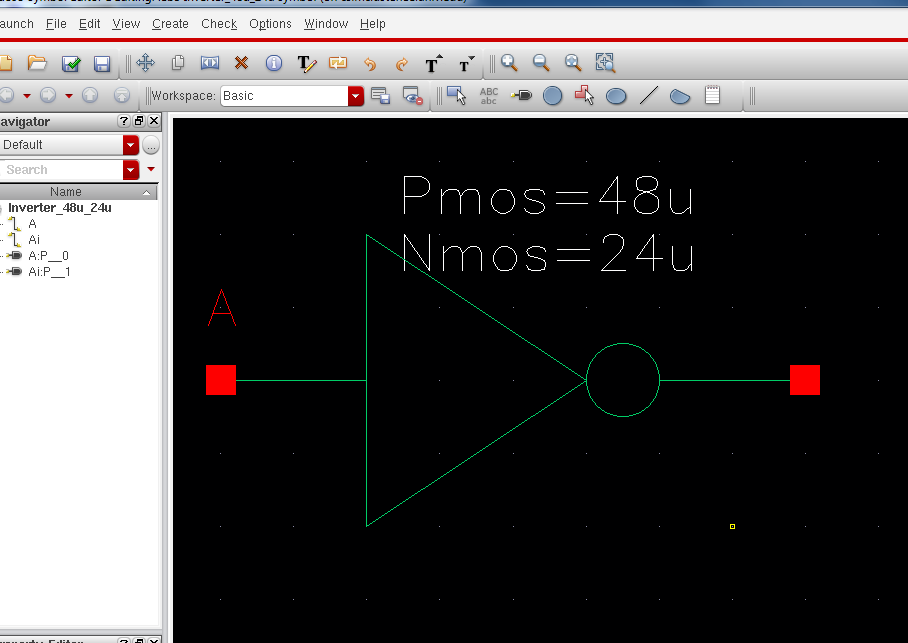
| symbol of a 48u by 600n Pmos and 24u by 600n Nmos. |
 |  |
| layout of a 12u by 600n Pmos and 6u by 600n Nmos. | layout of a 48u by 600n Pmos and 24u by 600n Nmos. |
 |  |
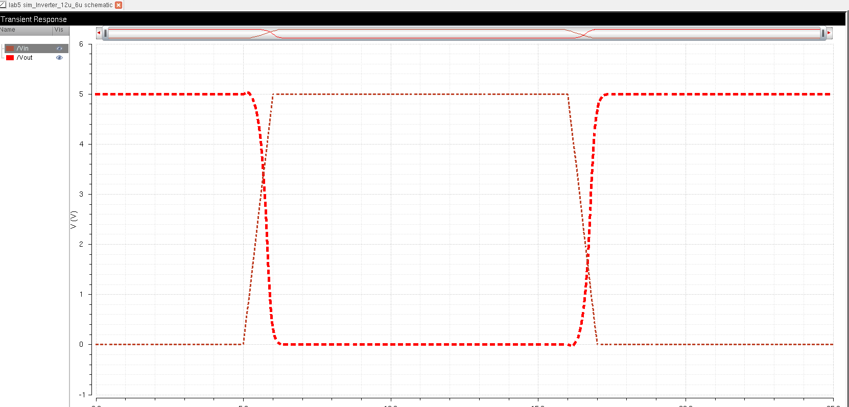
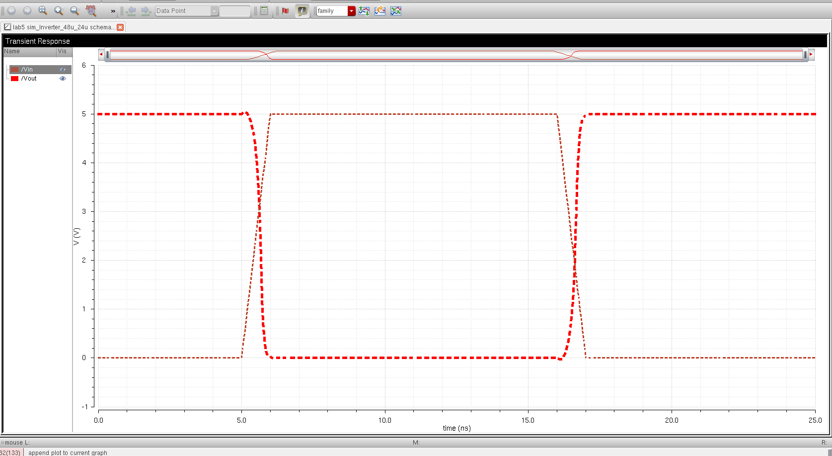
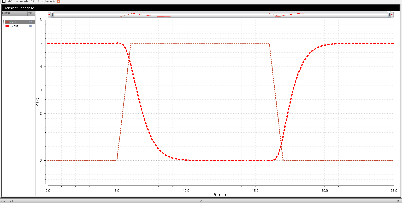
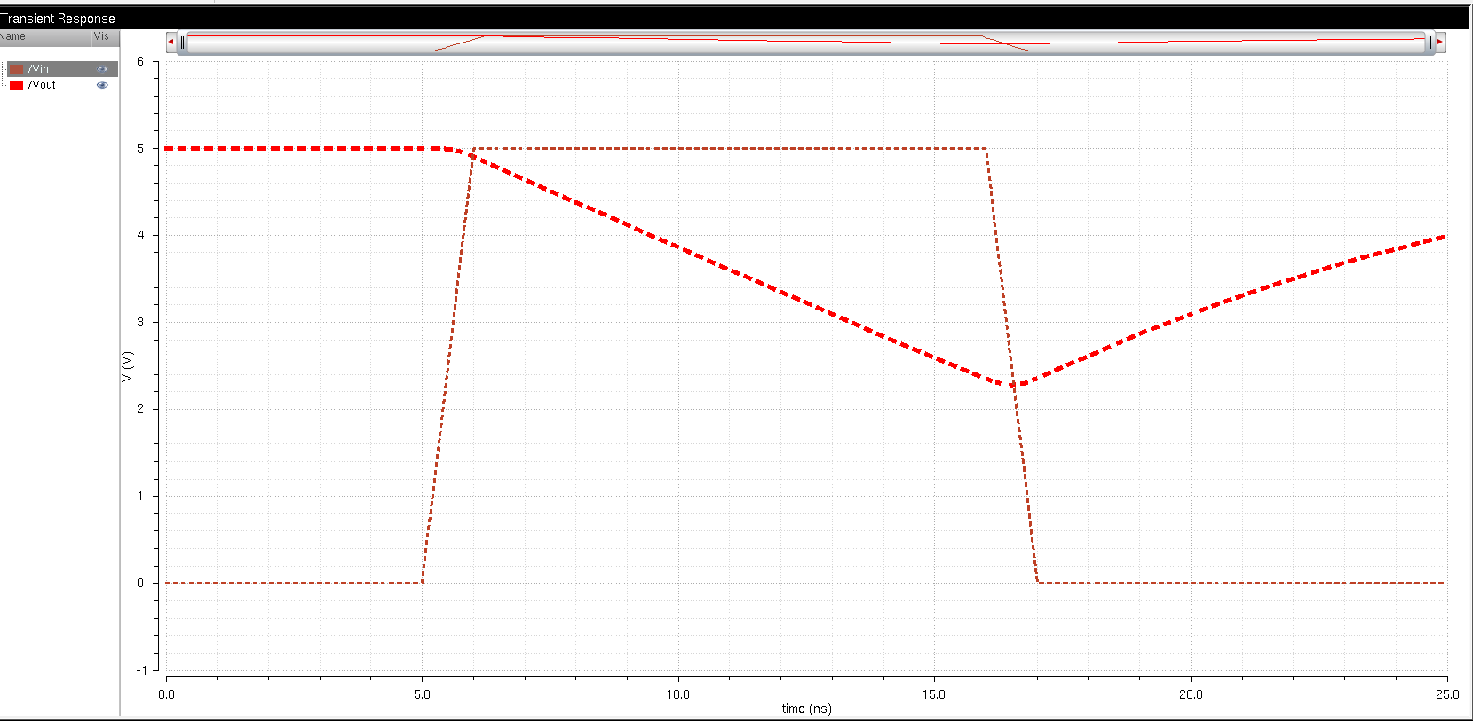
- Using SPICE simulate
the operation of both of your inverters showing each driving a 100 fF, 1 pF, 10 pF, and 100 pF capacitive load
- Comment, in your
report, on the results
| Adding a Capacitive load on the 12u/6u inverter | Adding a Capacitive load on the 48u/24u inverter |
 |  |
| C = 100 fF | C = 100 fF |
 |  |
| C = 1 pF | C = 1 pF |
 |  |
| C = 10 pF | C = 10 pF |
 |  |
| C = 100 pF | C = 100 pF |
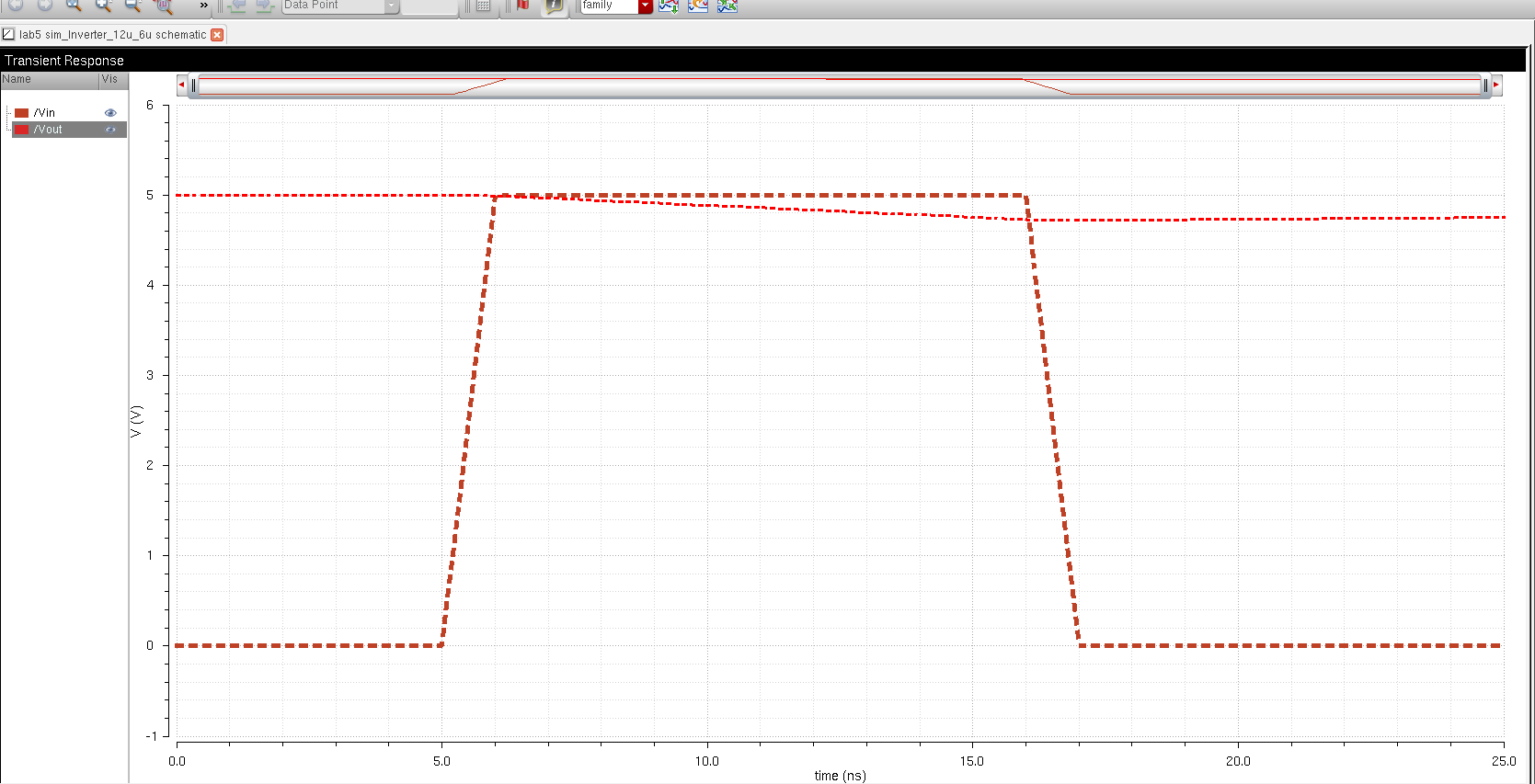 |  |
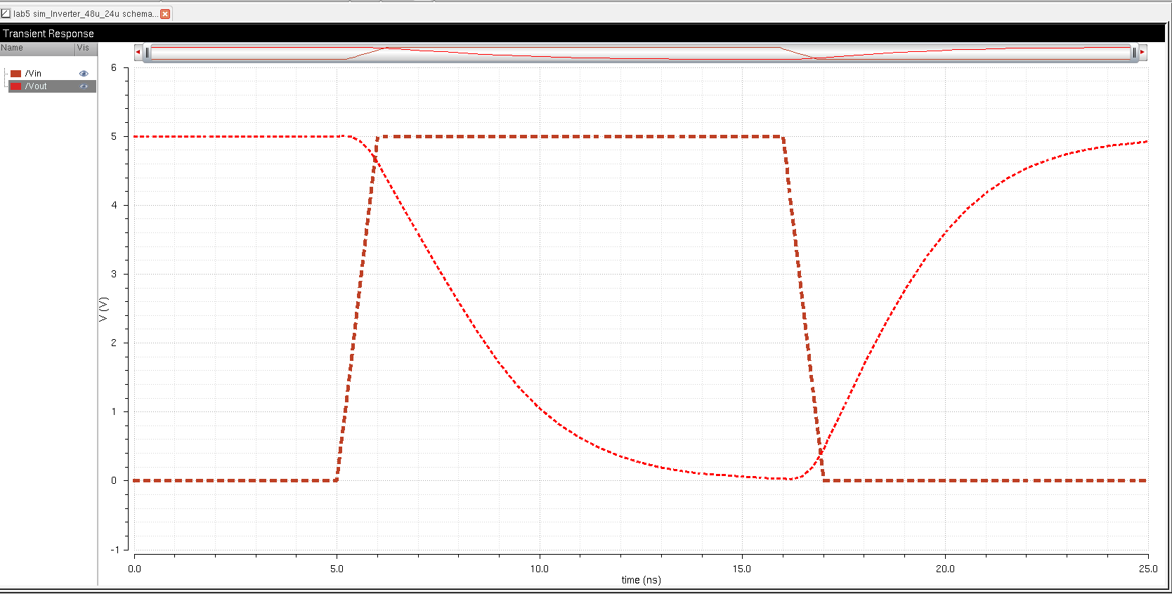
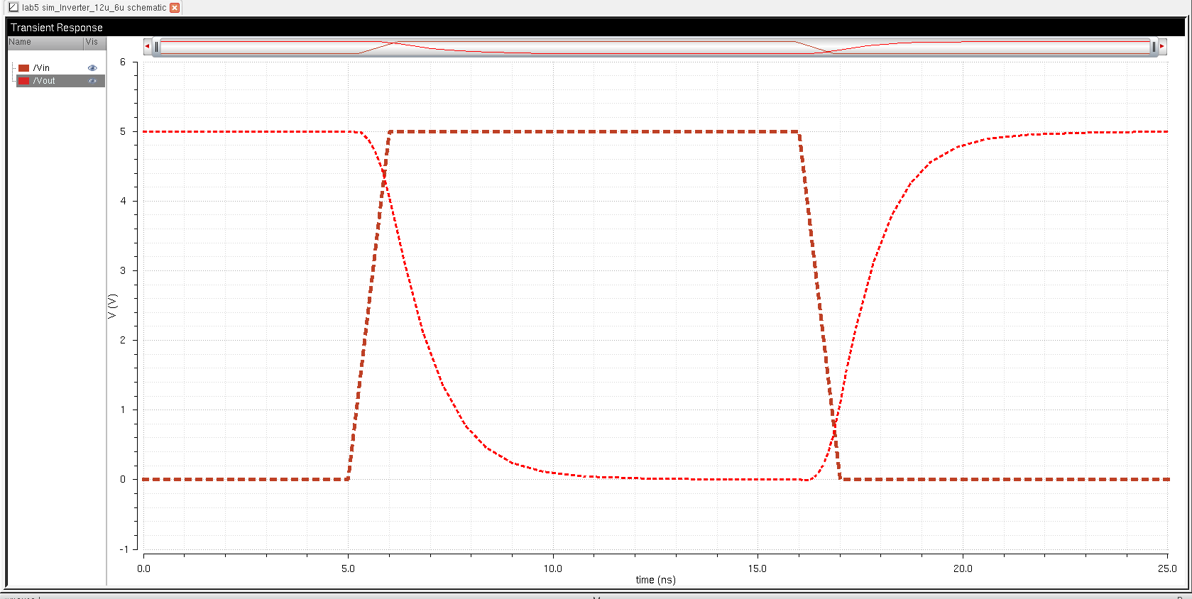
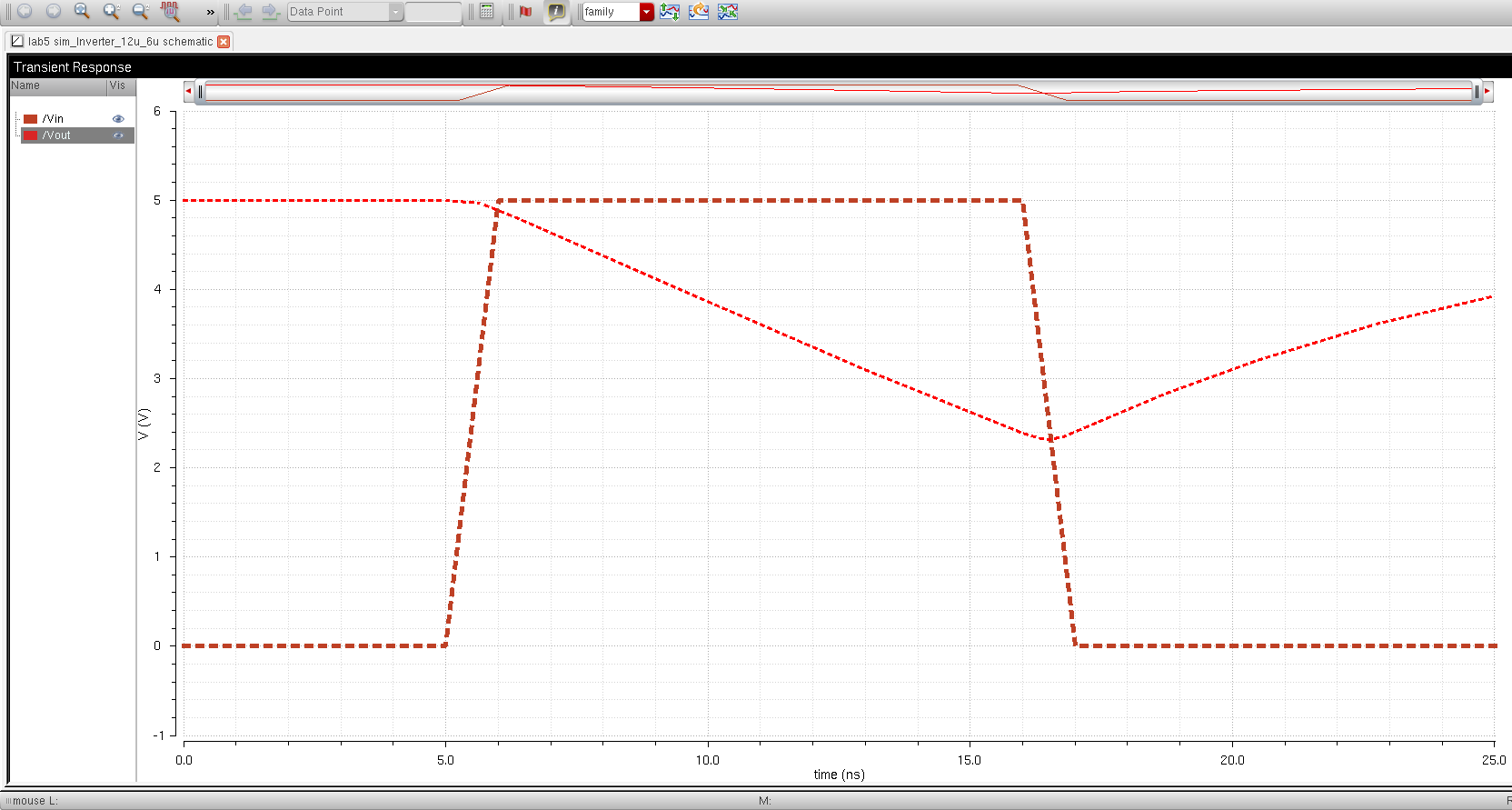
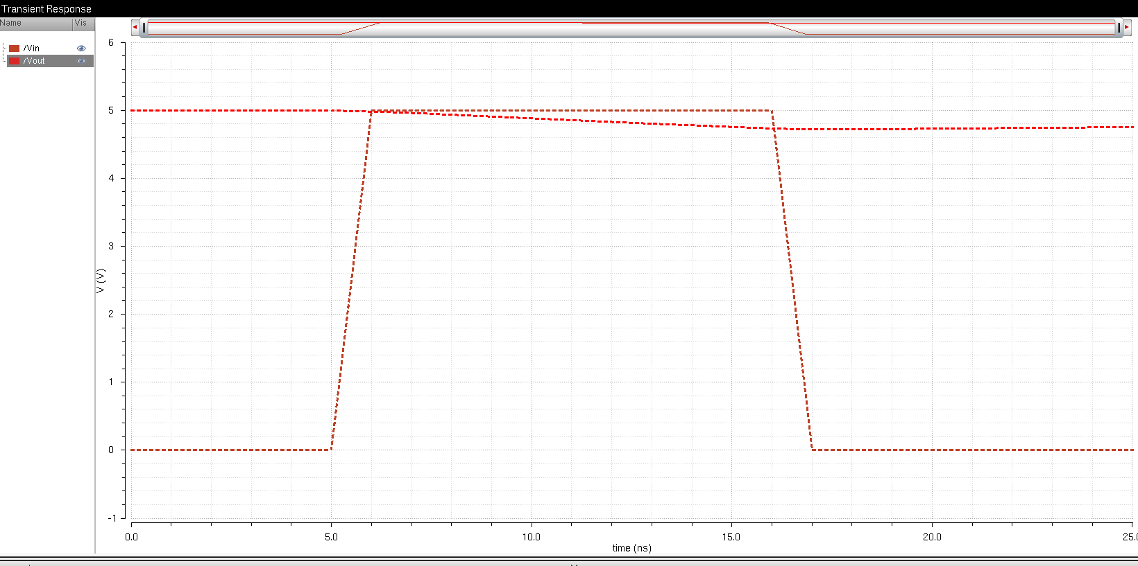
When
the capacitor is small the respond time for both the 12u/6u is the same
as the 48u/24u, but when the capacitor is higher the respond time for
the 48u/24u is much more accurate and precise compare to the the
12u/6u. you can see from the graph that at C=100pF for the 12u/6u
MOSFET the inverter does not even invert, its output will become a
constant number when you put a higher capacitance in there. for the
48u/24u MOSFET there is still some inversion at the c=100pF.
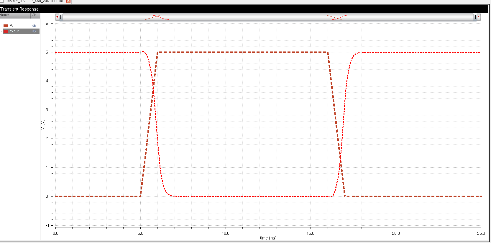
- Use UltraSim (Cadence's fast SPICE simulator for larger circuits at the cost of accuracy) and repeat the above simulations
- Use Setup -> Simulator/Directory/Host and select UltraSim as seen below
- You'll also have to point to the MOSFET models again as seen below
- Note that UltraSim only performs transient simulations (not AC, Noise, DC, operating point, etc.)
- Not knowing this last item will lead to wasted time if trying to use UltraSim exclusively for simulations
| 12u/6u Inverter | 48u/24u Inverter |
| C = 100f F | C = 100f F |
 | |
| C = 1p F | C = 1p F |
 | |
| C = 10p F | C = 10p F |
 | |
| C = 100p F | C = 100p F |
 |
|
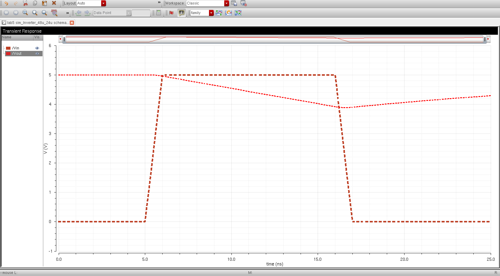
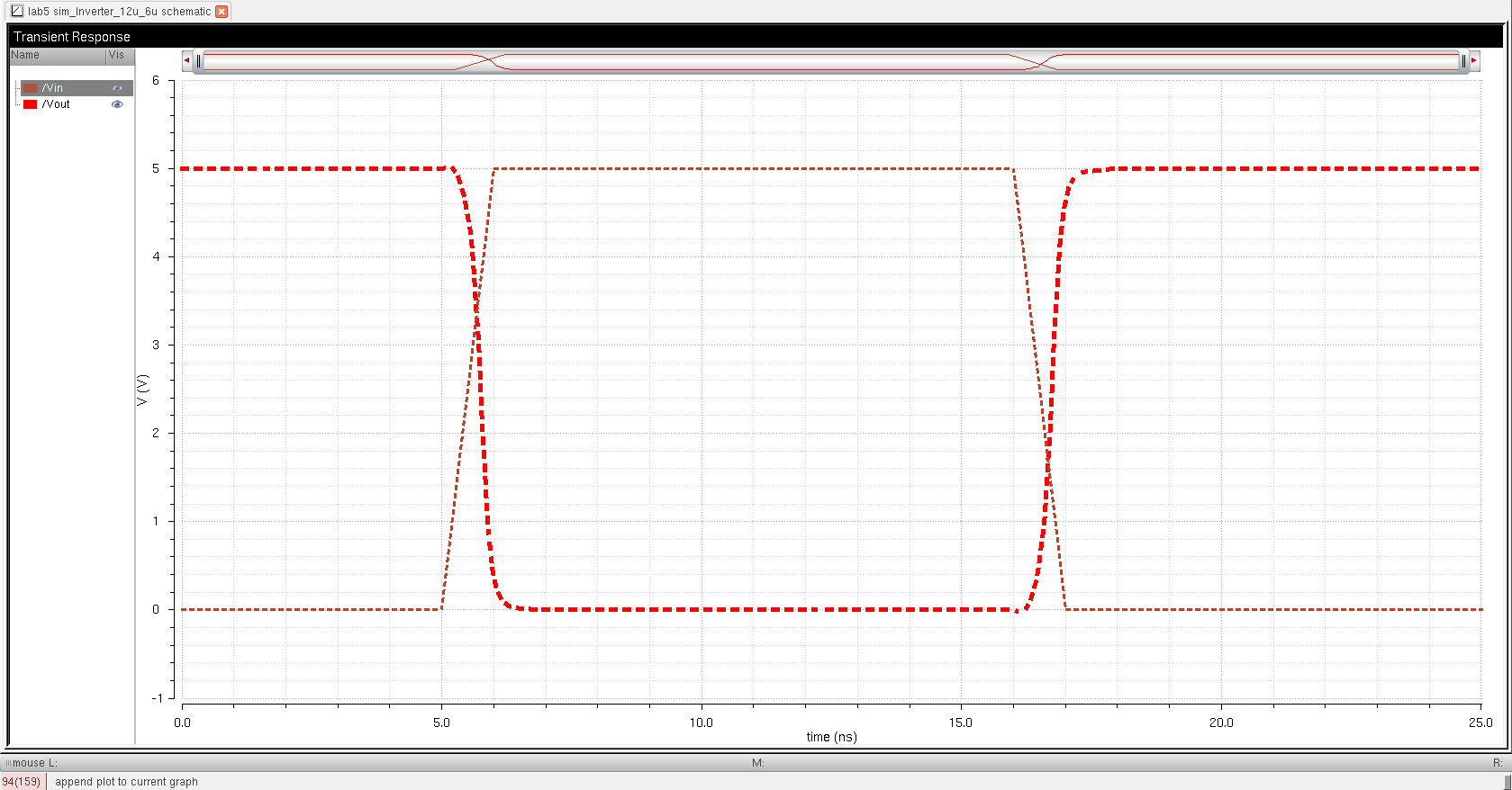
The
ultrasim and the spectre simulation gives the same results as can be
seen from the graphs. Again similar to the explanation above When the capacitor is small the respond time for both the 12u/6u is the
same as the 48u/24u, but when the capacitor is higher the respond time
for the 48u/24u is much more accurate than the 12u/6u.
lab5.zip cadence work.
THIS ENDS LAB5
zipping up the lab folder and the lab5.html and emailing it.
Return to EE 421L labs