Lab 4 - EE 421L
Authored
by Nha Tran
Email: trann4@unlv.nevada.edu
NHSE ID: 2000590233
10/06/2014
Lab objective: The purpose of this lab to draw the characteristics and layout of NMOS and PMOS devices using the C5 process.
Prelab:
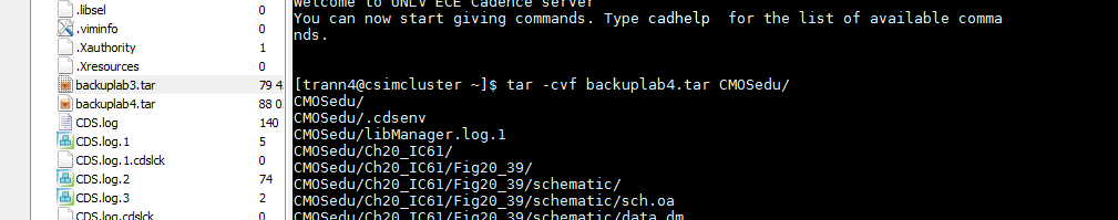
First create a backup of the work that was done previously in the class and lab by typing tar -cvf backuplab4.tar CMOSedu/ in the MobXterm command line. this command line back-ups all the data that is in the CMOSedu/ folder up until lab 4.
Next
start virtuoso in MobaXterm by typing cd CMOSedu/ then virtuoso &.
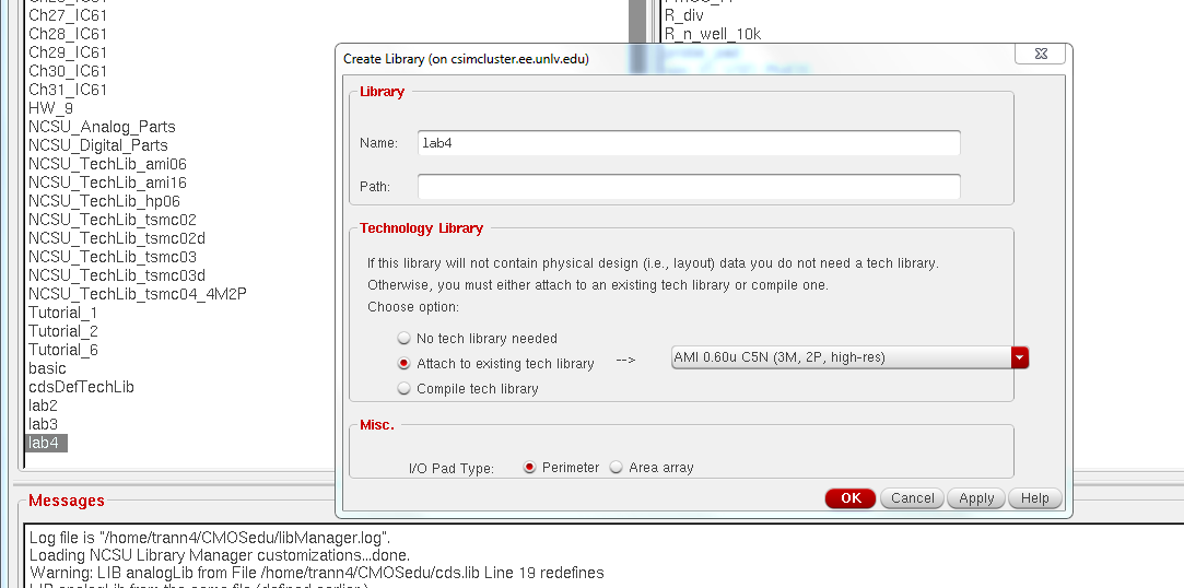
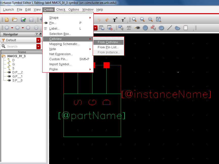
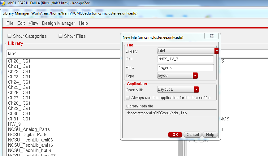
Once cadence is open, go to the library manager and click file -->
new --> library and name it lab 4, ass seen below.
Next
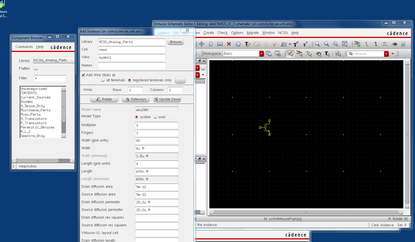
create a new schematic in the lab4 folder by going file --> new
--> cell view --> schematic, name is NMOS_IV_3. Once open
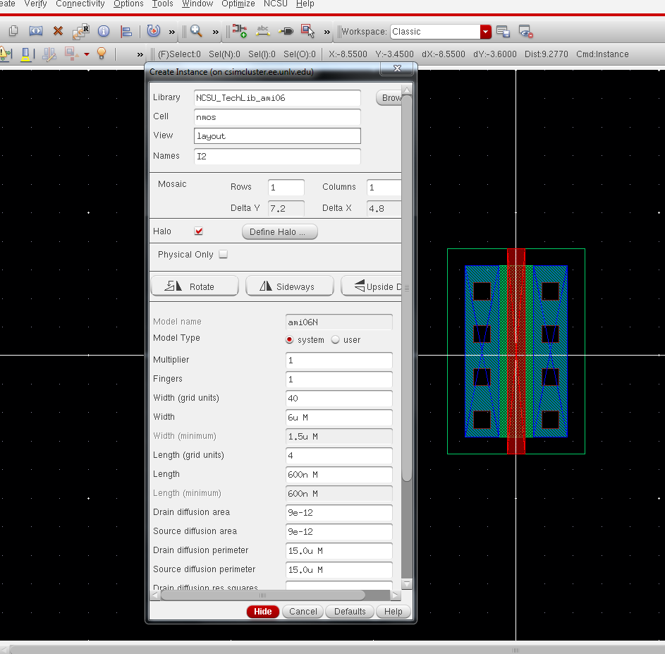
instantiate an nmos symbol by using keybind i then searching for the
nmos symbol in the NCSU_Analog_Parts, remember to set the width to 6u
and lenght to 600n. As seen below
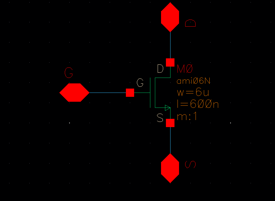
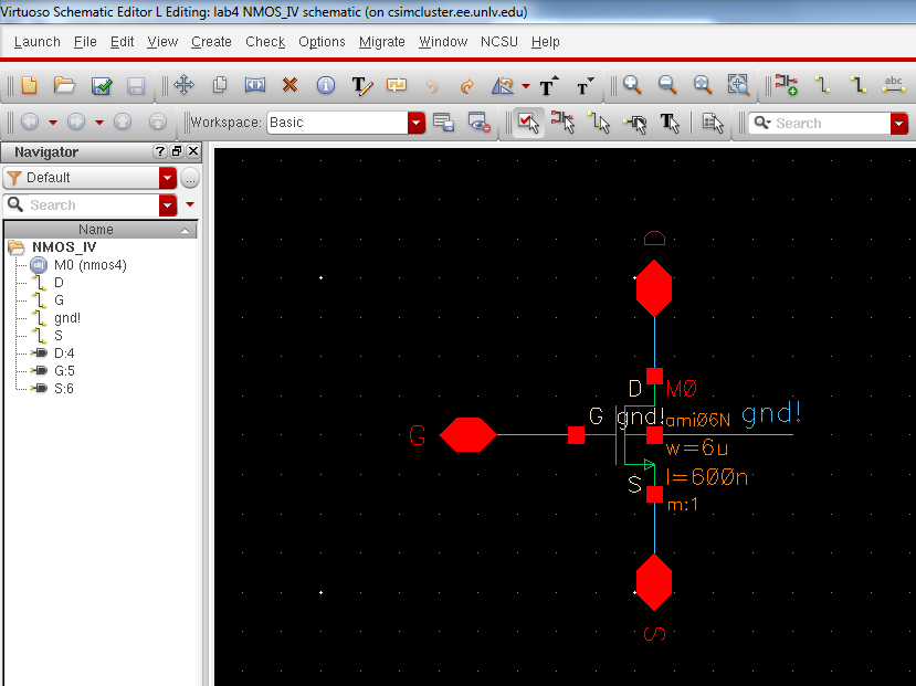
next create 3 pin D,G,S for drain, gate, source respectively by using keybind P. Adding wiring to connect the pins to the nmos
Save
the schematic, then go to create cell view from cell view. this will
create a symbol of the nmos device we create with the pins earlier.
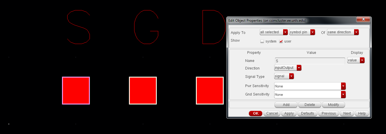
Next
delete everything but the 3 pins, then selecting all 3 pin and press
bindkey q to get its properties then select the box display value and apply to all selected
Next
draw the symbol of the MOSFET using the line by doing create -->
shape --> line. and adding the text W=6u and L=600n. similar to
below. check and save after finish.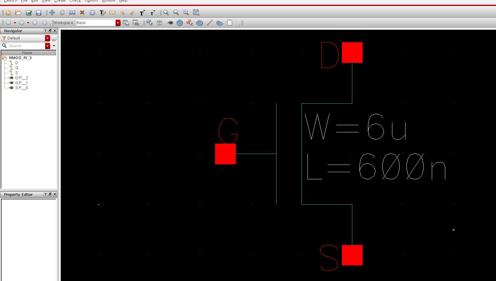
Next
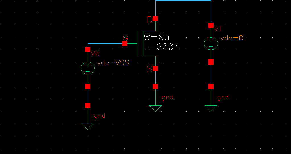
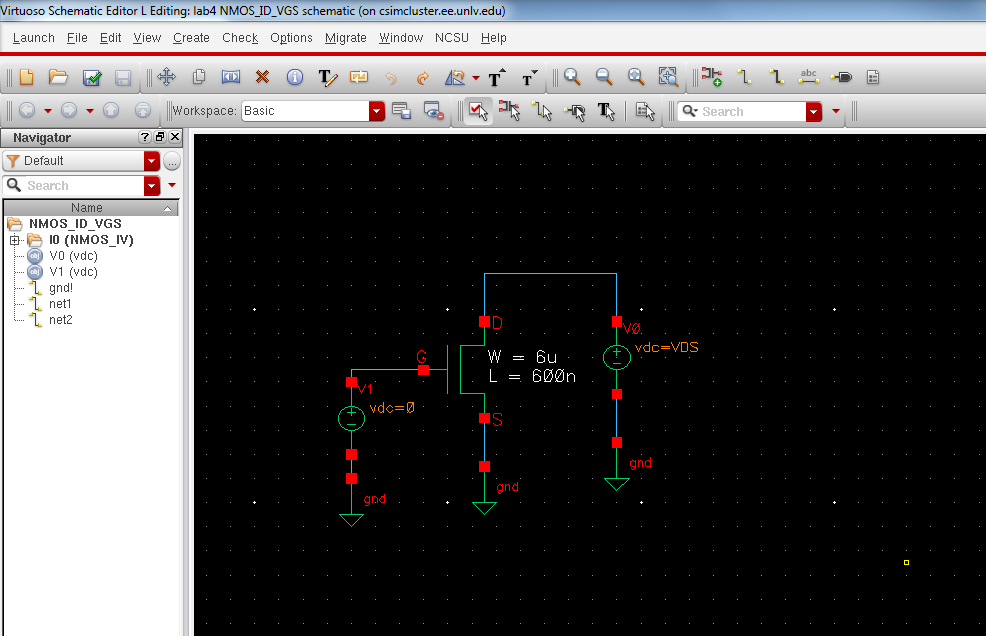
create a new schematic called sim_NMOS_IV_3. Instantiate the new nmos
symbol we just created and adding 2 voltage source and connect the
wires as seen below, setting V0 to VGS and v1=0
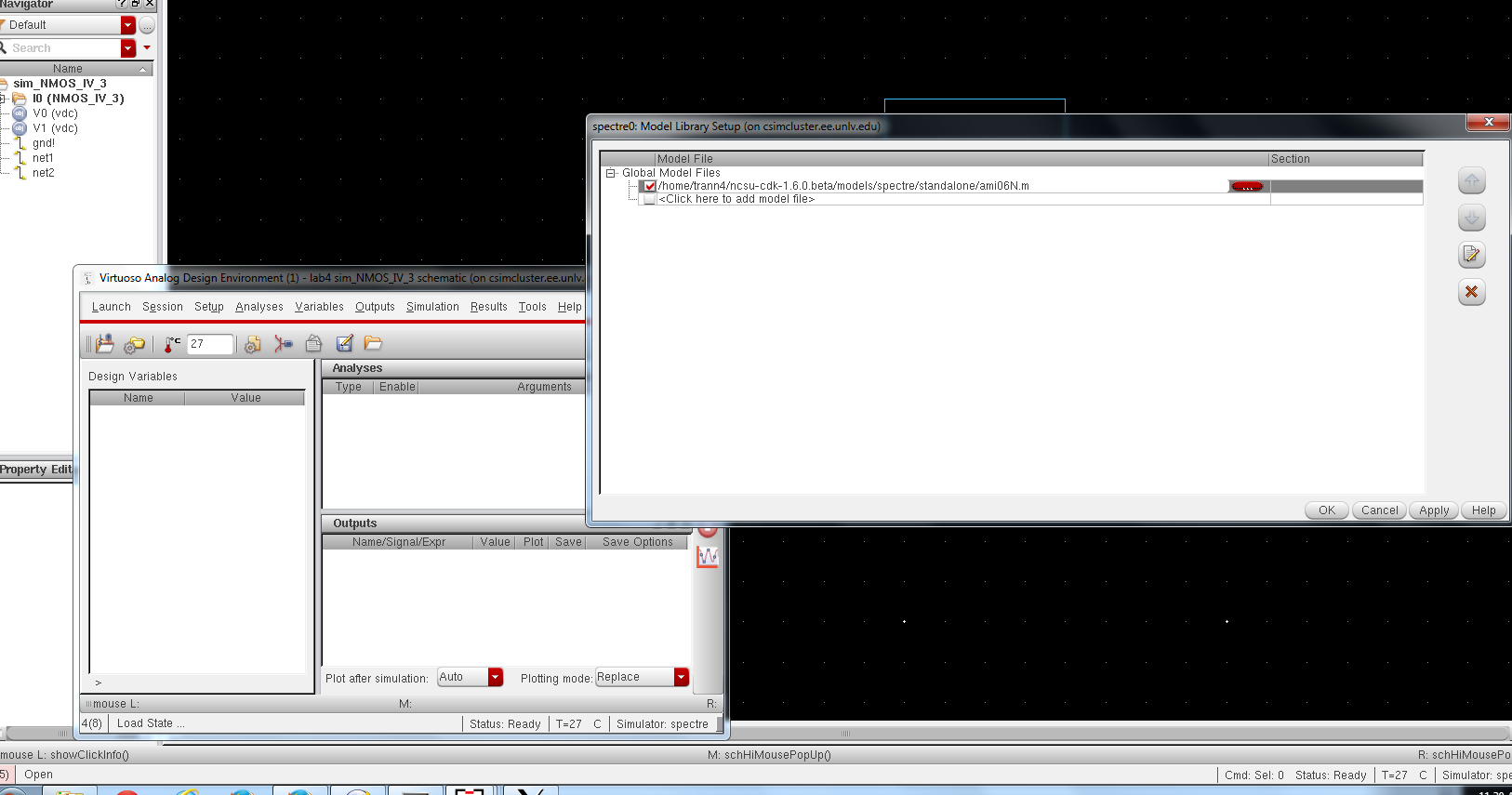
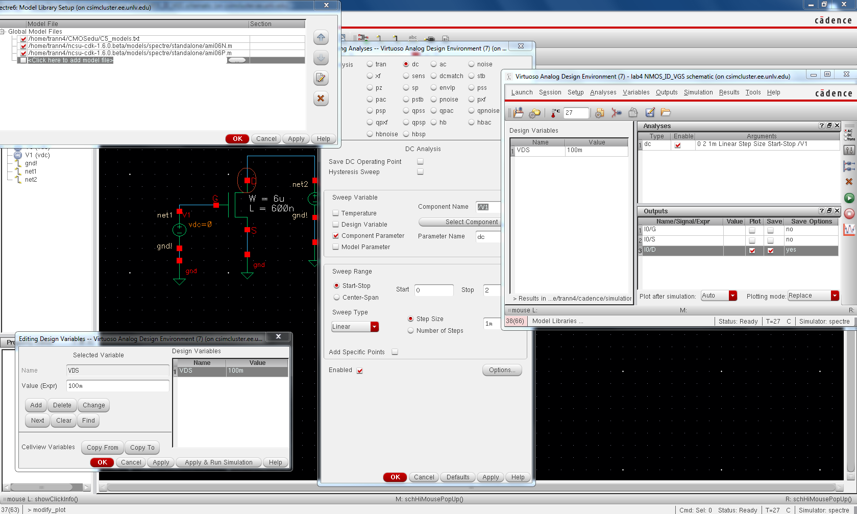
Launch ADE L, then go to setup --> model libraries and select this directory /$HOME /ncsu-cdk-1.6.0.beta/models/spectre/standalone/ami06N.m then click ok
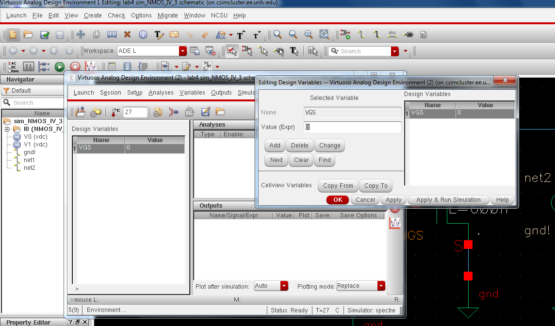
Next go select Variables --> Edit, then type the VGS for name and set the value to 0, as seen below.
next
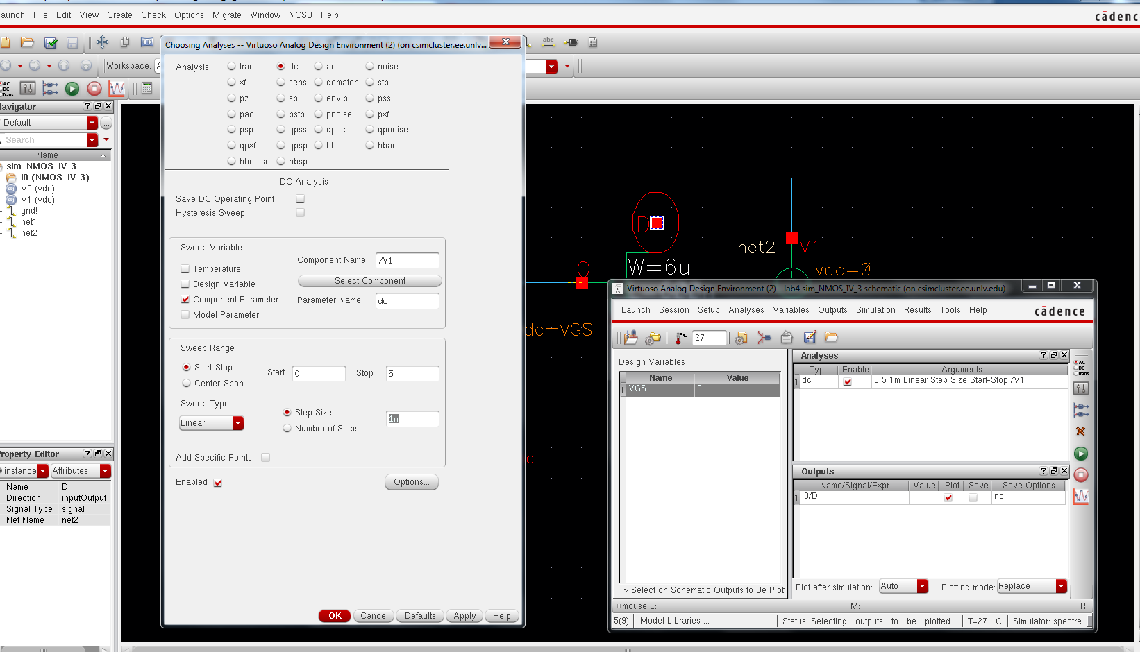
select dc analysis then select all the parrameter as seen below.
remember to set the parameter name is dc and component to /V1. then
select the output to be plotted and select the current for the drain
(D). and also save the simulation state.
Next select tools --> Parametric Analysis and set the parameter as seen below.
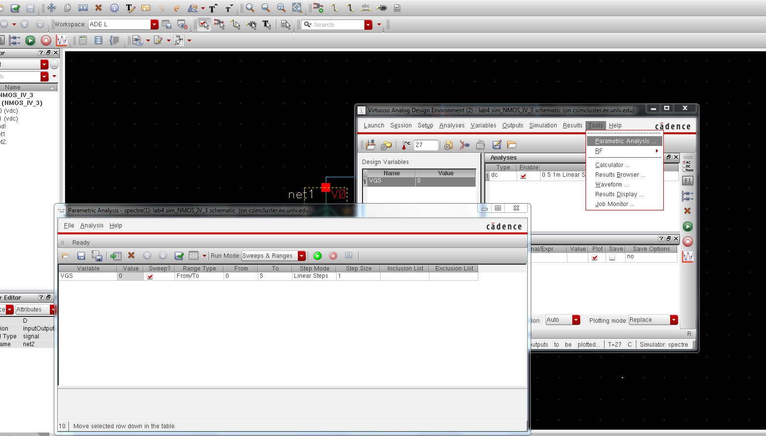
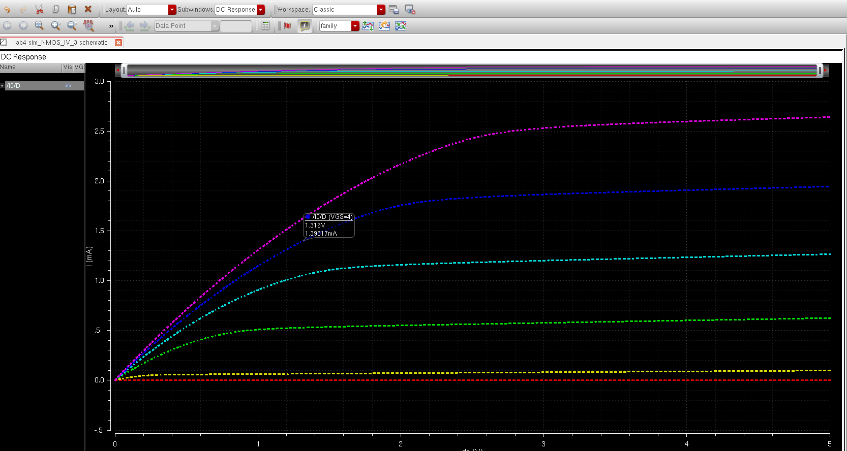
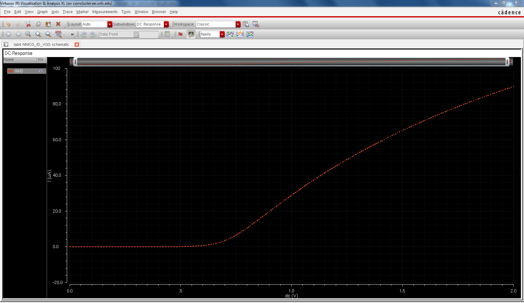
Then running the simulation you should get a sweep of the current across D similar to the image below.
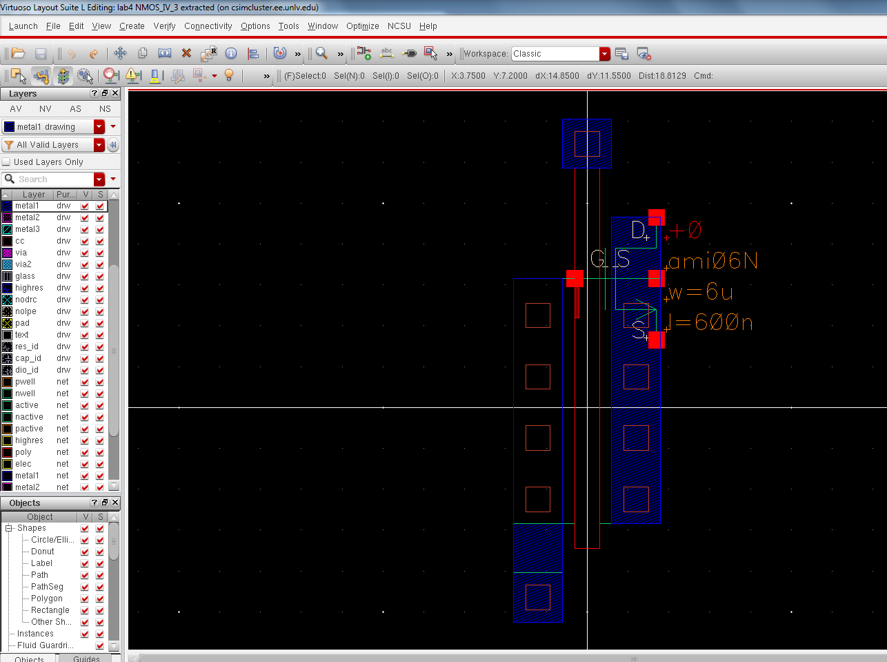
next create a new layout view of the NMOS_IV_3.
Instantiate the nmos layout by typing I then using all the paramater as seen below.
instantiate
a ptap cell which is the metal1 connect to the p+, and add a metal1
layout to connect the source to the p-substrate like below, also add a
metal1 to the drain side, then add a poly to melal1 (m1_pol) and add a
poly layer connecting the gate to the m1_poly.Add pin names A,D,G using
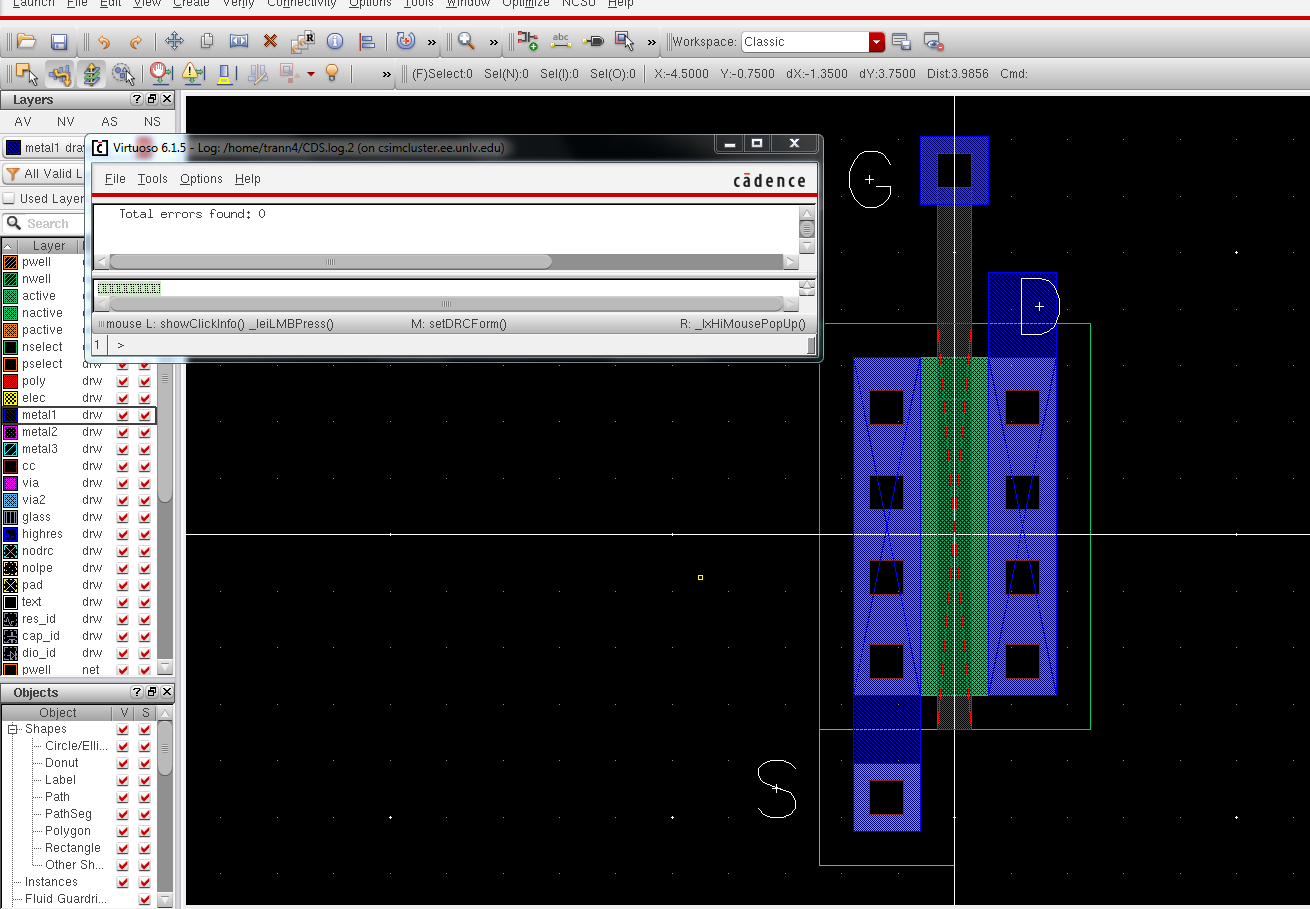
metal1 layer like below. and lastly DRC the layout, you can see it
DRC-ing gave zero errors.
Next
extract the layout you can see that it is an nmos device with 4 pins.
the body of the nmos is directly connected to the p-substrate.
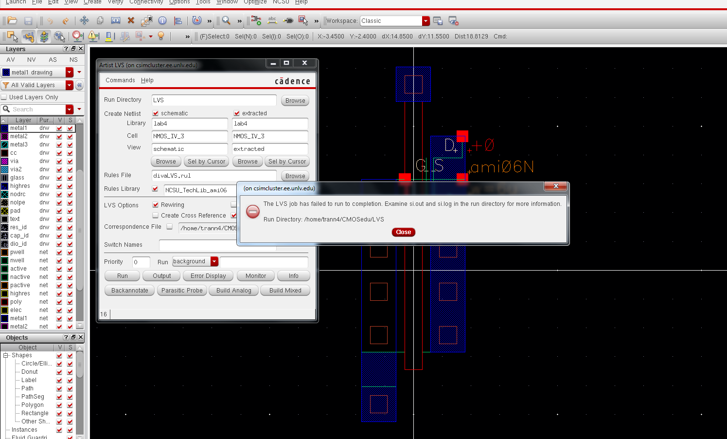
LVS
the layout and it will give us an error seen below, this error occur
because of how the bulk or the p-substrate is connected for the Nmos.
when using the 3 terminal MOSFET it is assumed that the bulk is tied to
the gnd for the NMOS and vdd for the PMOS.
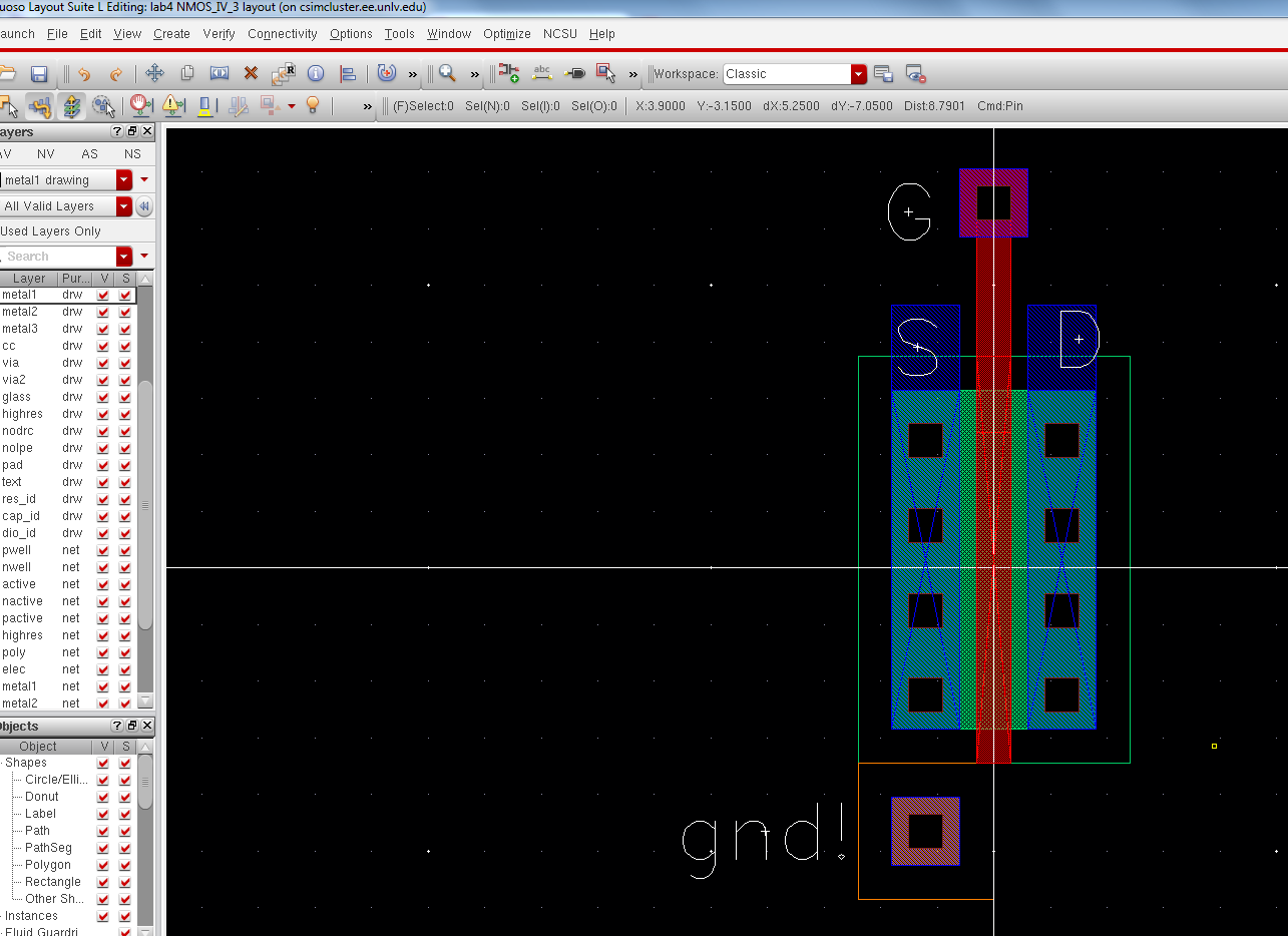
to
fix this problem deleted the metal1 layer connecting the p-tap to the
Source. and connect the S to the bulk. and add a pin to make the p-tap
= gnd! as seen below.
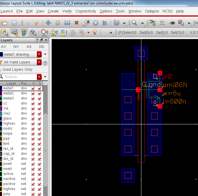
extract the layout and it should look like below.
LVS-ing
will gaive an another error, this is because of the nodal name for the
terminal of the nmos device that we are using. the program wants us to
use a 4-terminal transistor in the schematic. so close all cellview
and, copy NMOS_IV_3 to NMOS_IV, and sim_NMOS_IV_3 to sim_NMOS_IV. open
the NMOS_IV and change it to look like below.
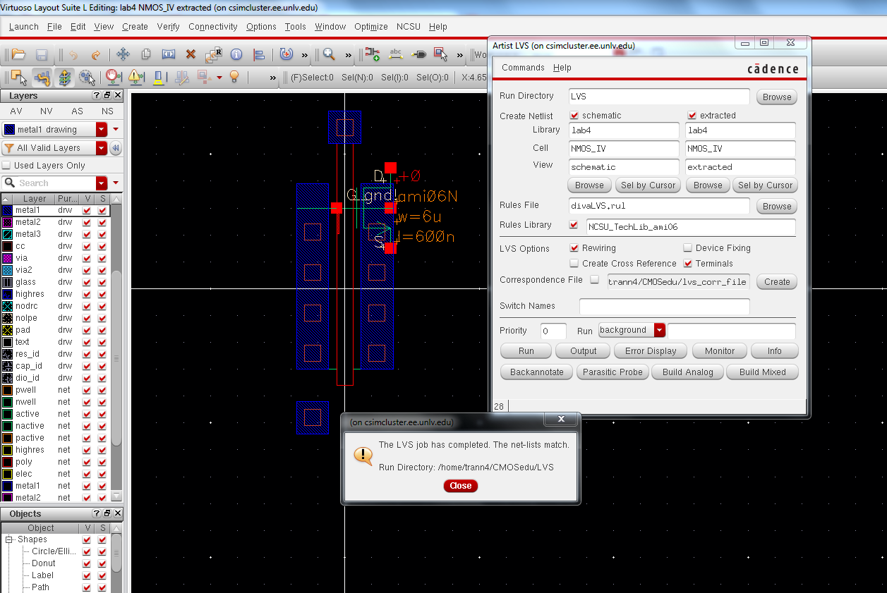
Now open the extracted view and LVS it like below. now the schematic matches the extracted.
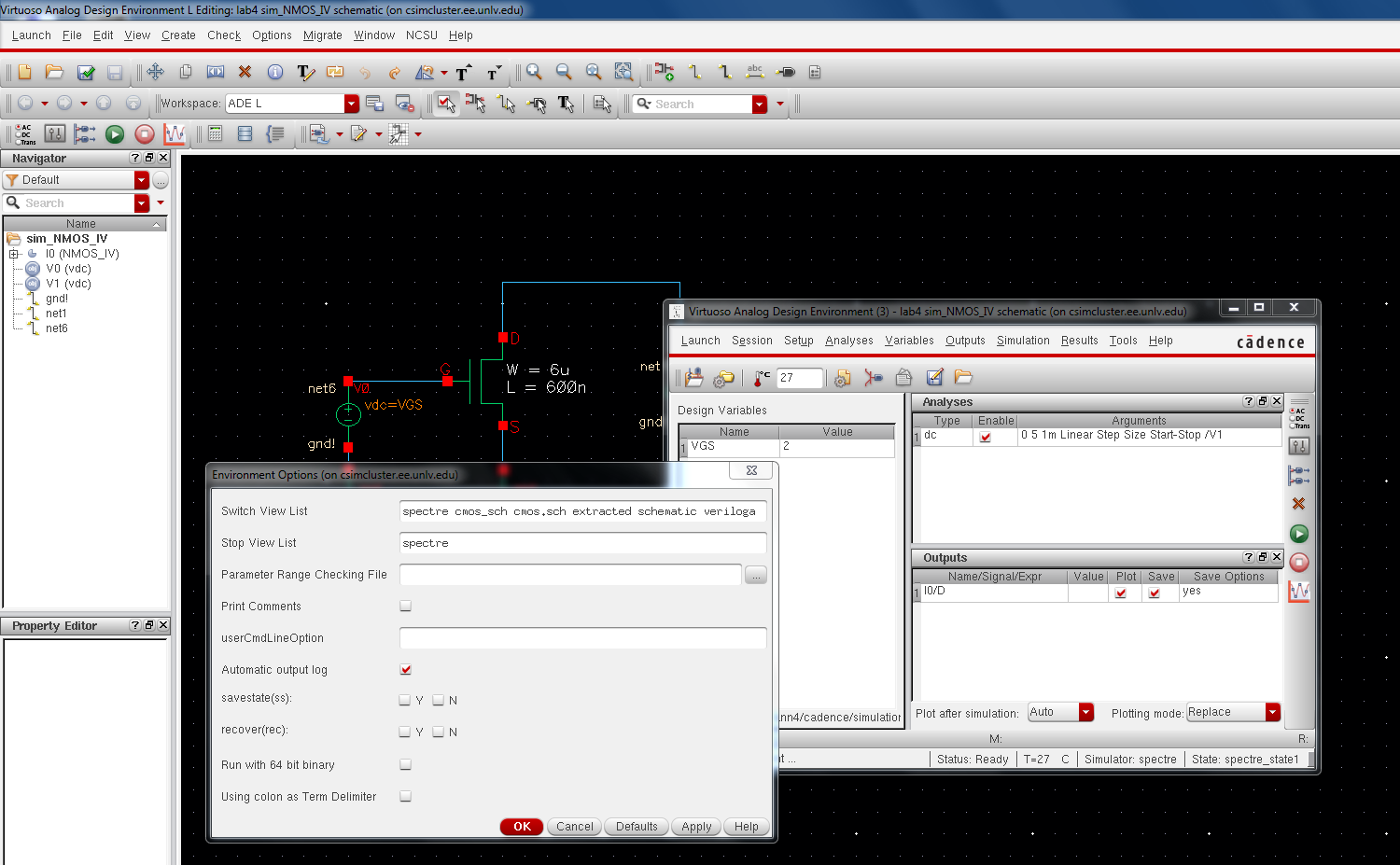
Now
open the schematic of the sim_NMOS_IV, run ADE L, then go to sessions
load states, then go to setup --> environment and type the word
extraced before schematic as seen below.
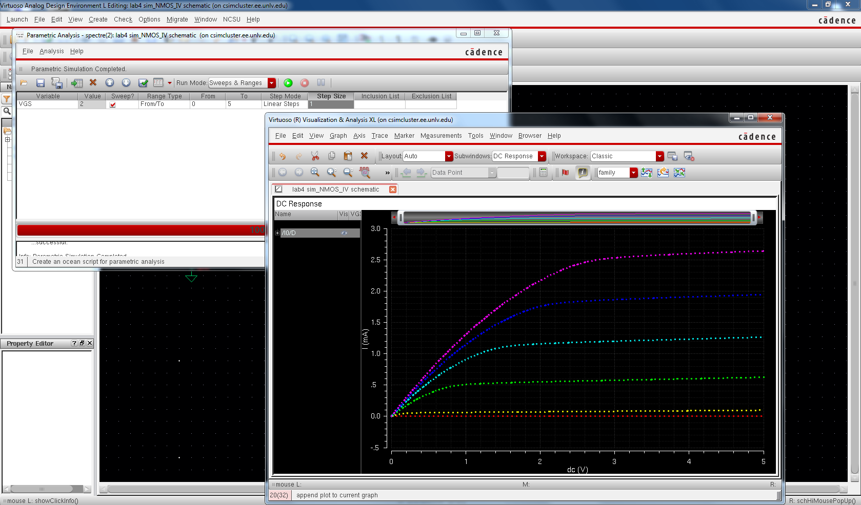
Lastly go to parametic analysis and enter the values as seen below, and run the simulation you should get a graph like below.
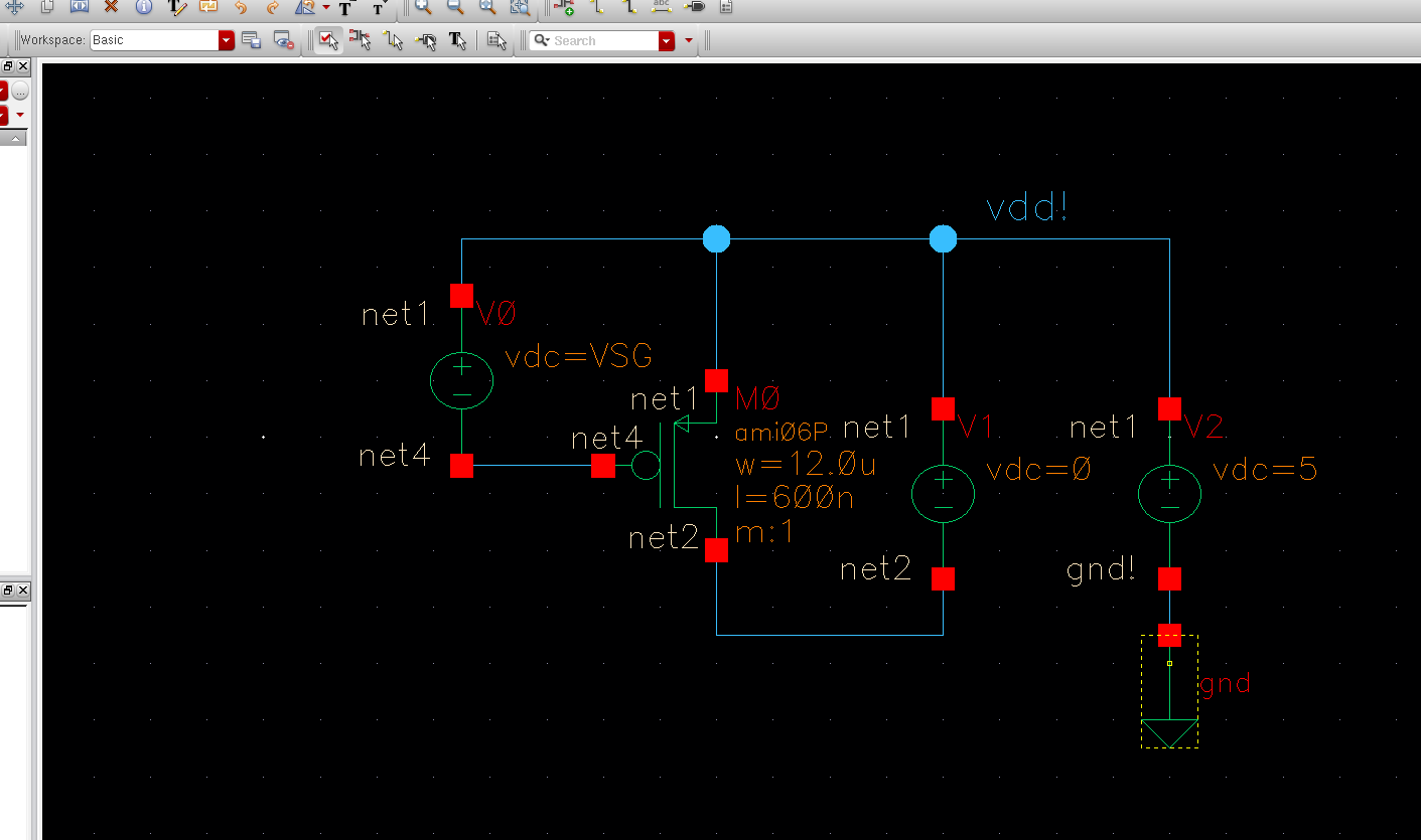
Save everything and create a new cellview call PMOS_IV and create a device with 4 pins like below
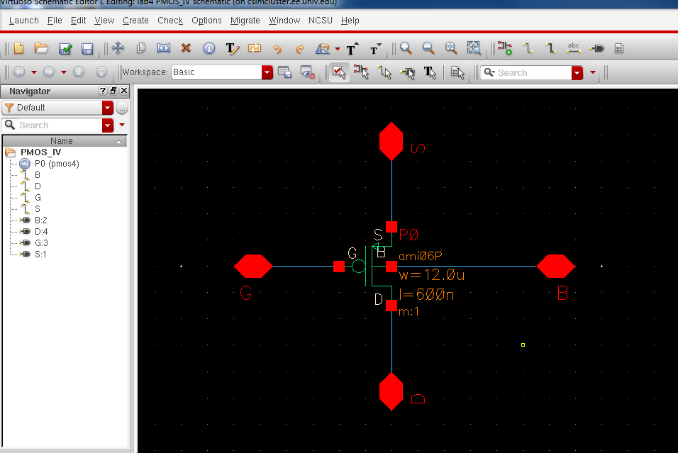
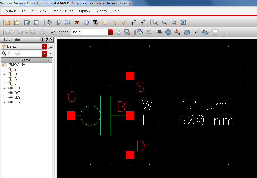
next create a symbol for the PMOS like the one we did for the NMOS like below
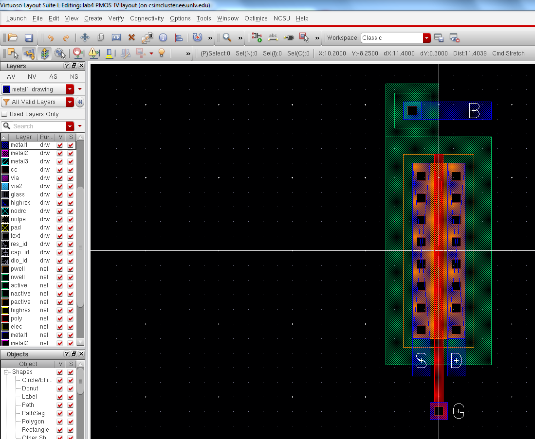
Next create a layout of the PMOS like below.
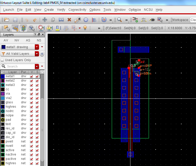
 Next extract the layout of the PMOS device.
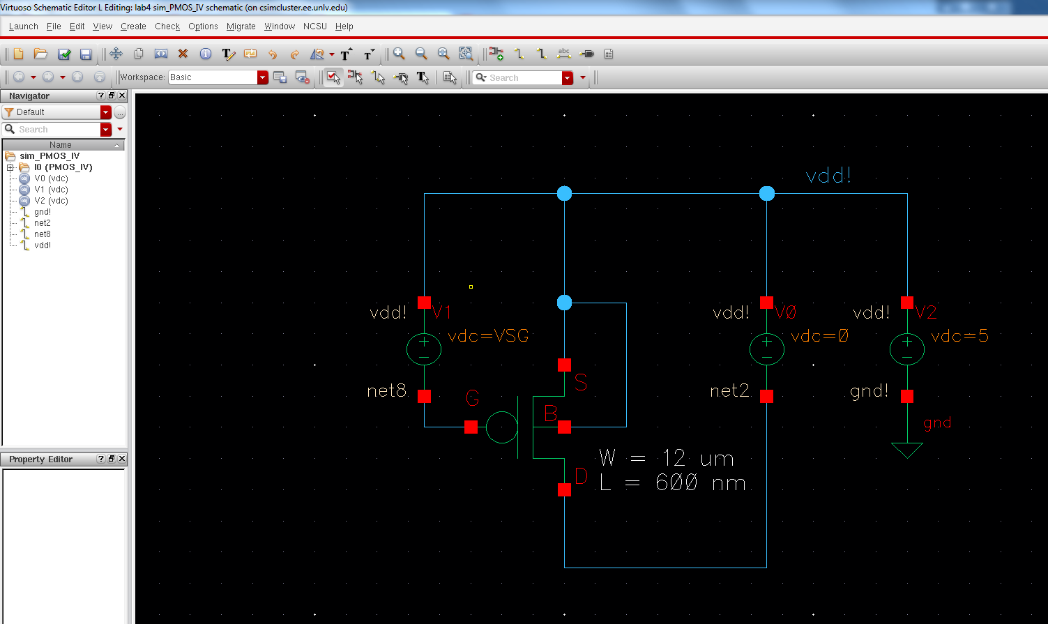
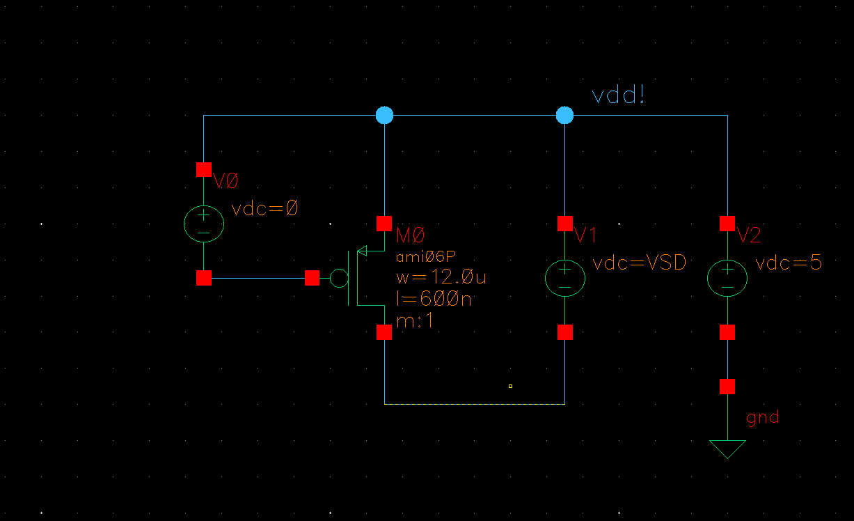
next create a new cellview and name it sim_PMOS_IV and create the circuit as seen below.
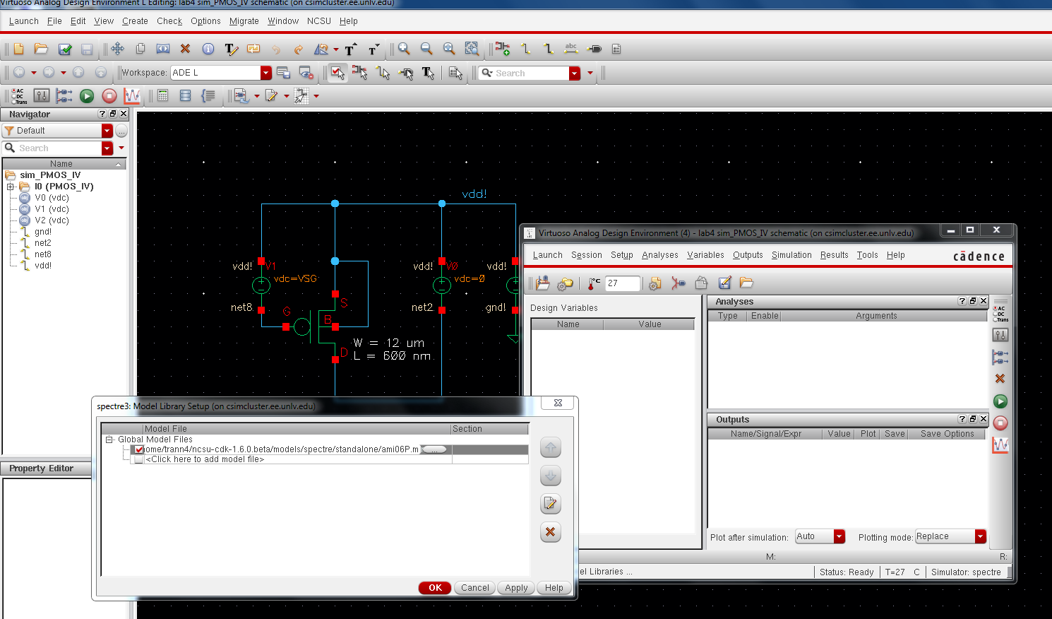
Now we ready to simulate the shematic, run ADE L, then go to setup --> model libraries and set the model as seen below.
Then
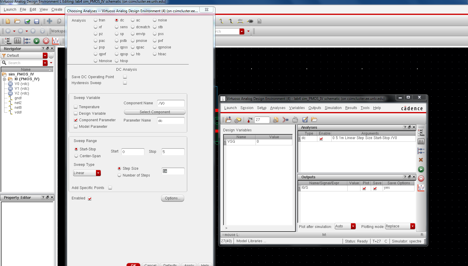
go to variables --> Edit and set the name to VSG and the value to 0.
Now go to plotted and select S to be plotted. next go to analysis and
choose dc and enter the following values.
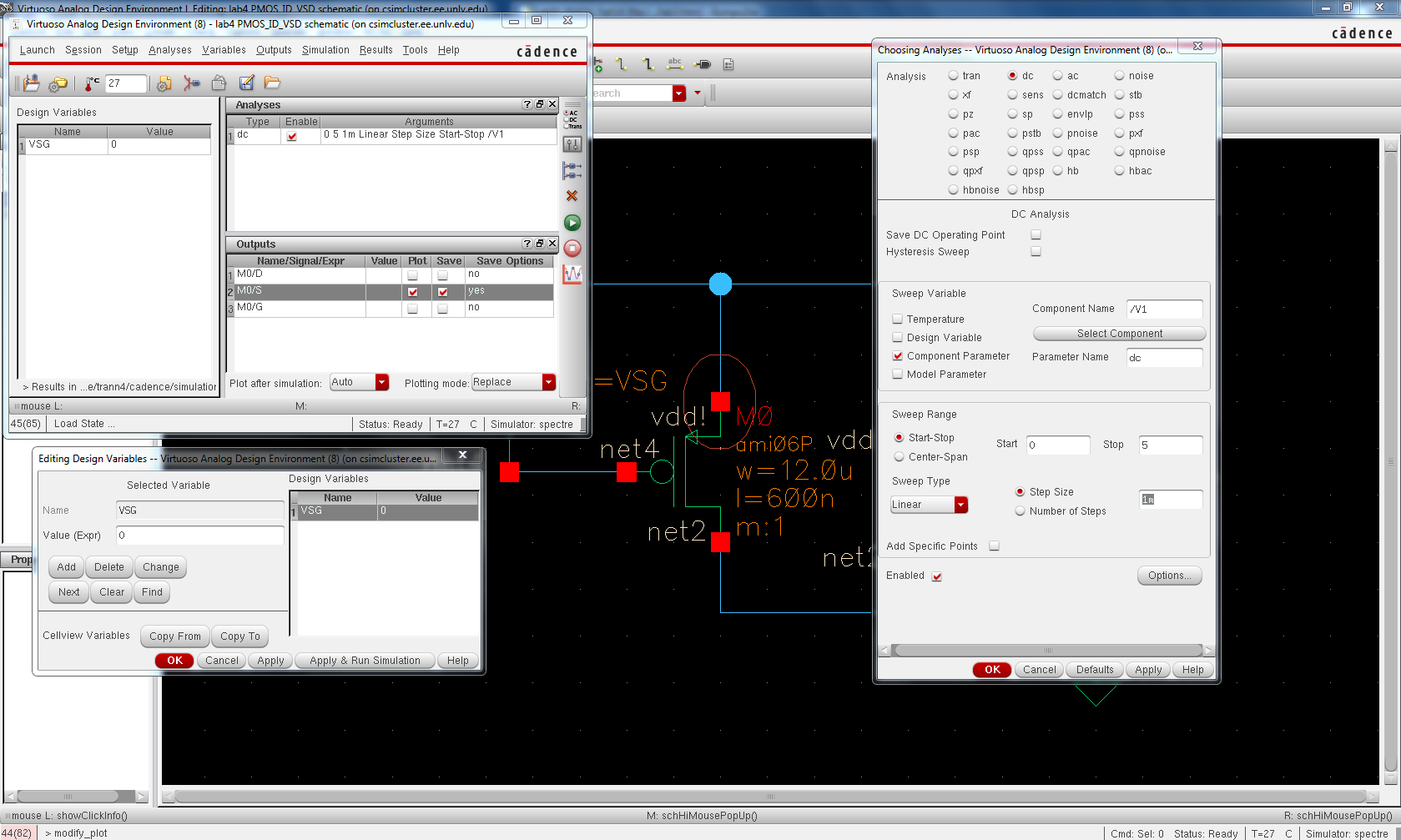
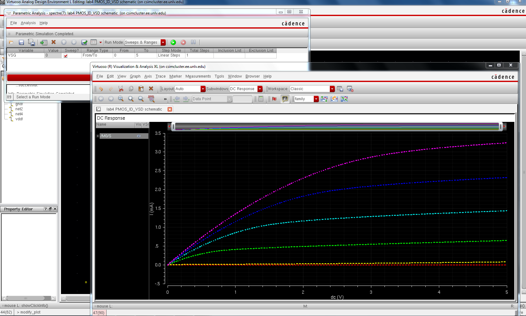
Go
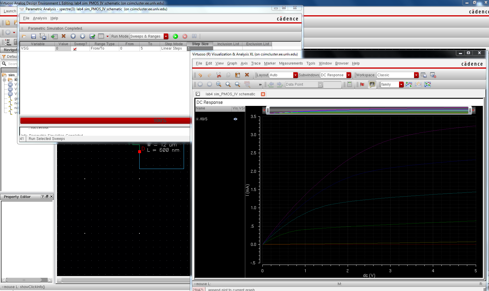
to tools then go to parametric analysis, and input the values as seen
below and then select run and you will get the graph of the sweep of
the S like below.
next
lets simulated the extracted view by going setup --> environment
then add the word extracted before schematic like we did above for the
NMOS device. and running the sim we should get a graph that looks
exactly the same as the one above. to make sure that we are using the
extracted view as our sim we can check by going simulation -->
netlist --> display and we see that the view name is indeed the
extracted view which is highlighted in the below image.
END PRELAB
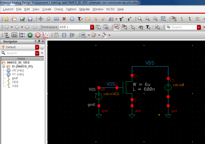
- A
schematic for simulating ID v. VDS of an NMOS device for VGS varying from
0 to 5 V in 1 V steps while VDS varies from 0 to 5 V in 1 mV steps. Use a 6u/600n width-to-length ratio.
run
ADE L, go to variables --> Edit and set the name to VGS and the
value = 0, go to setup --> model libraries and add the libraries as
seen below, then go to analysis and choose dc set the variable as seen
below
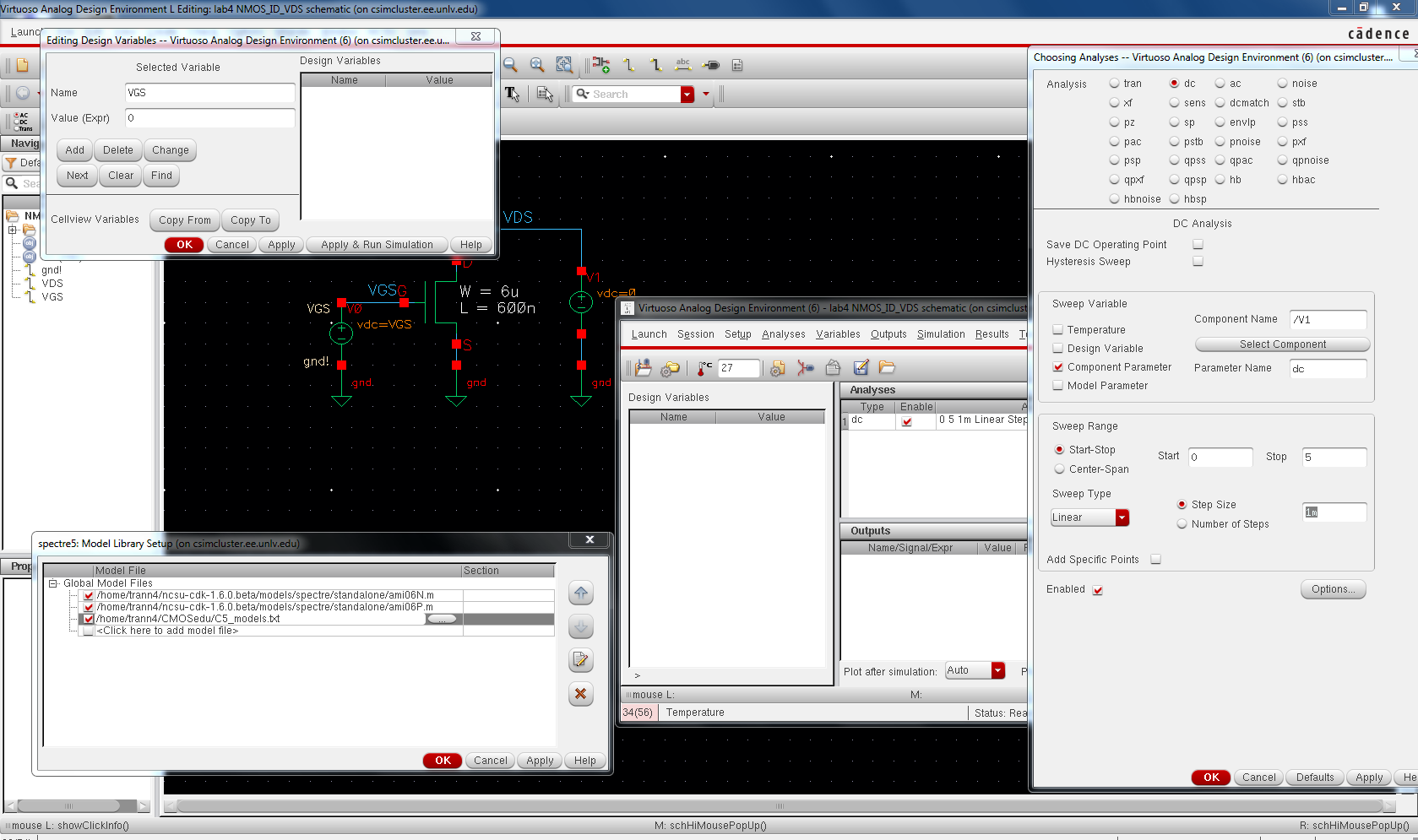
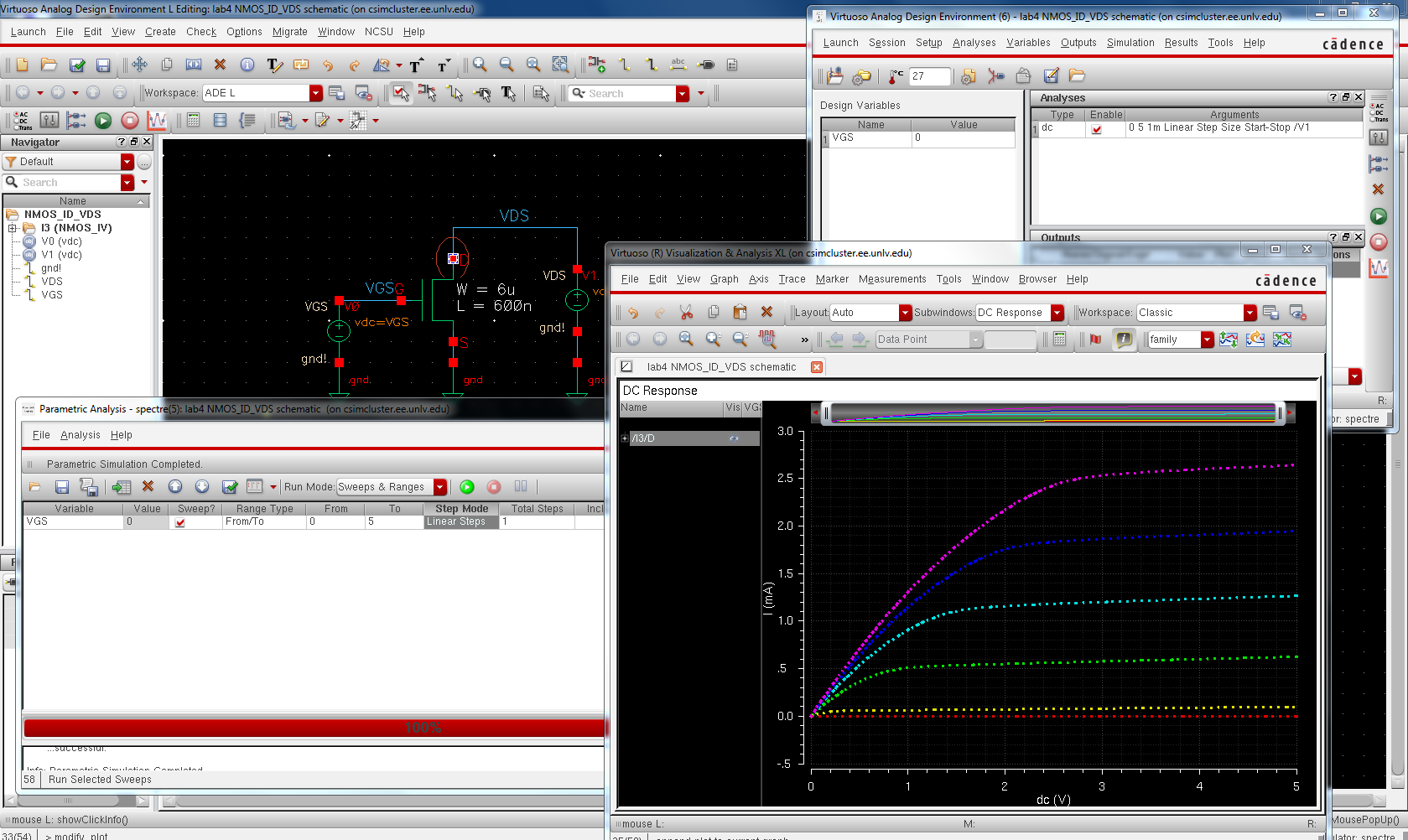
next
select the current through the Drain that we will be plotting. Then go
to tools --> Parametric analysis and input the values as seen below.
and select run and the output graph should look like below.
- A
schematic for simulating ID v. VGS of an NMOS device for VDS = 100 mV
where VGS varies from 0 to 2 V in 1 mV steps. Again use a 6u/600n width-to-length ratio.
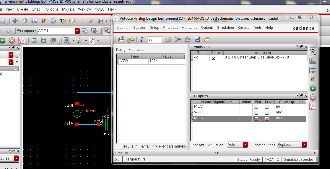
Setting
the model library like before, choose the dc analysis and selecting the
parameter like below, and setting the variable name VDS to 100m
selecting run you should get a graph that look similar to the one below.
- A
schematic for simulating ID v. VSD (note VSD not VDS) of a PMOS device
for VSG (not VGS) varying from 0 to 5 V in 1 V steps while VSD varies
from 0 to 5 V in 1 mV steps. Use a
12u/600n width-to-length ratio.
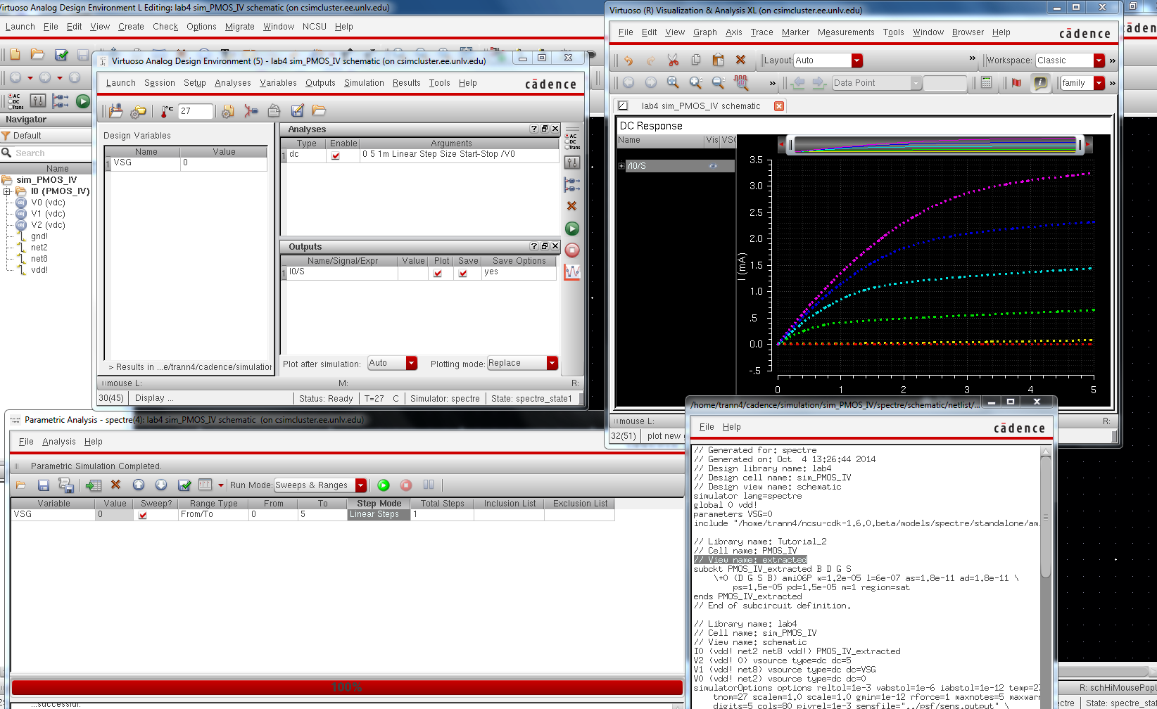
again setting the parameter below, choose S to be plotted, and choose dc analysis and setting all the parameter like below.
seeting the parametric analysis below and running the sim you should get a graph like below
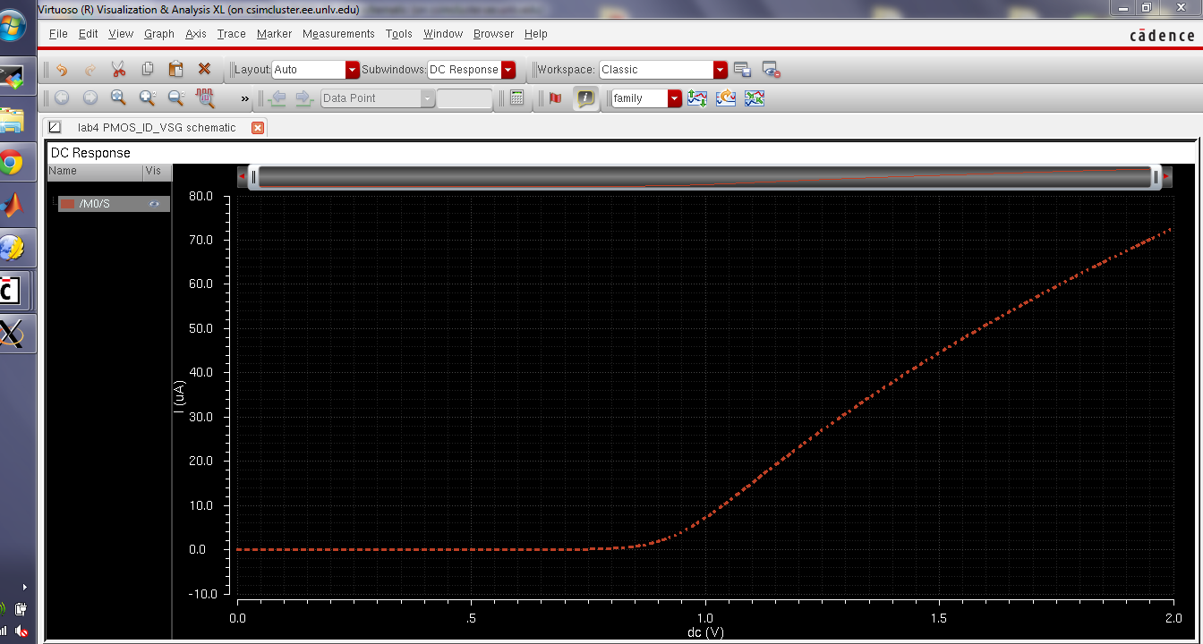
A
schematic for simulating ID v. VSG of a PMOS device for VSD = 100 mV
where VSG varies from 0 to 2 V in 1 mV steps. Again, use a 12u/600n width-to-length ratio.
Selecting the parameter as shown below following the procedure that was done like the previous steps.
And hitting netlist and run and the graph should be like below
- Lay out a
6u/0.6u NMOS device and connect all 4 MOSFET terminals to probe pads
(which can be considerably smaller than bond pads [see MOSIS design rules]
and directly adjacent to the MOSFET (so the layout is relative small).
- Show your layout passes DRCs.
- Make a corresponding schematic so you
can LVS your layout.
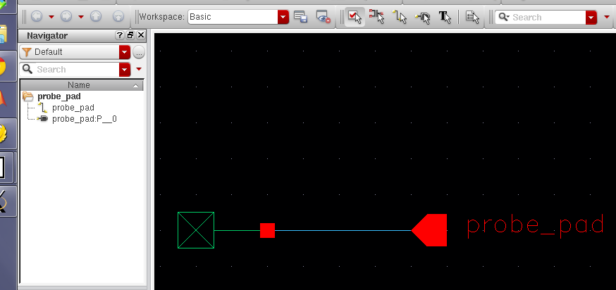
Now
we need to create a probe pad, first create a new cell view schematic
and name it probe_pad. Create an instance (keybind I) and find the
instance in basic --> misc --> noconn. Now make a pin and connect
to it as shown below.
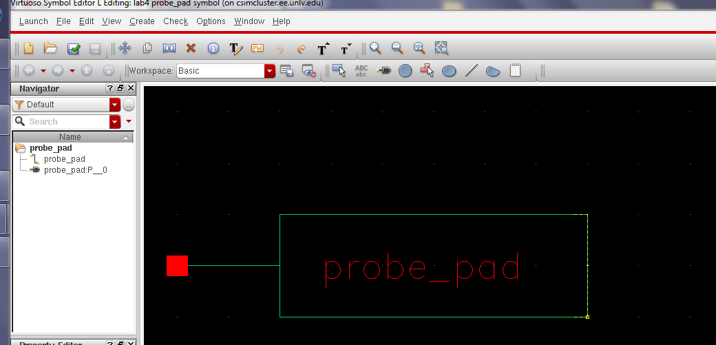
Now
create a symbol out of the schematic that we just create. go create
--> cellview from cellview and our symbol for the probe pad should
look like below.
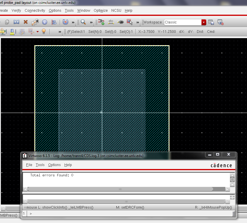
Next
we want to create a layout of our probe pad. Start by selecting metal3
and drawing a box, then keybind q and changing the dimension to 33.6 by
33.6. Then draw a box on the glass layer center on the metal3 layer
with the dimension 21.6 by 21.6. Finally DRC-ing the layout to show
that it gives zero error.
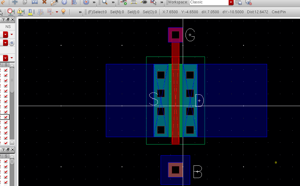
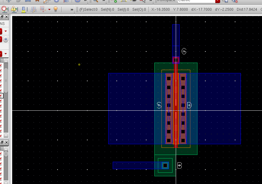
Next
create a new layout call NMOS_4pin. Then instantiate an Nmos4 from the
ami06 library. Remember to set the W=6u and L=600n. i used metal1 layer
to add the pin S,D,G,B to connect to the nmos, i used a m1_poly layer
to connect the G, and for B i used a ptap.
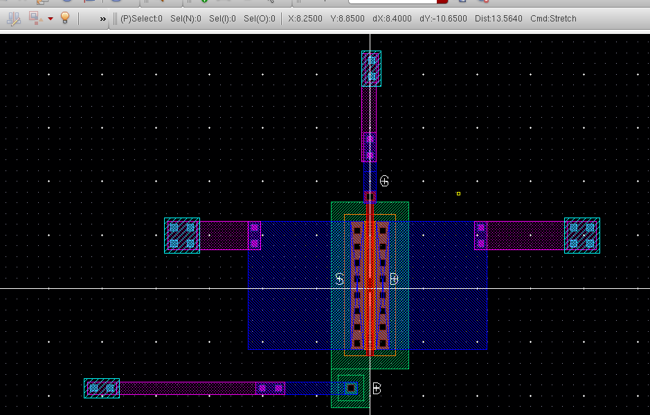
now
since the probe_pad is made with a metal 3 layer we need to connect the
pins S,D,G,B from M1 to M2 then M2 to M3. we can do this by first
instantiate m2_m1 and connecting it to our 4 pin. then we want to add a
m3_m2 layer to connect from metal 3 to metal 2.
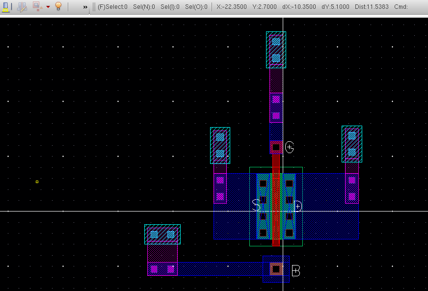
Now instantiate the probe pad and connect the metal 3 layer to our probepad. and DRC-ing you see that there is no error
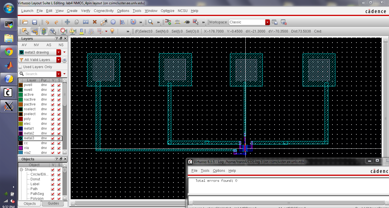
next extract the layout view. below is the zoomed in view of the extracted nmos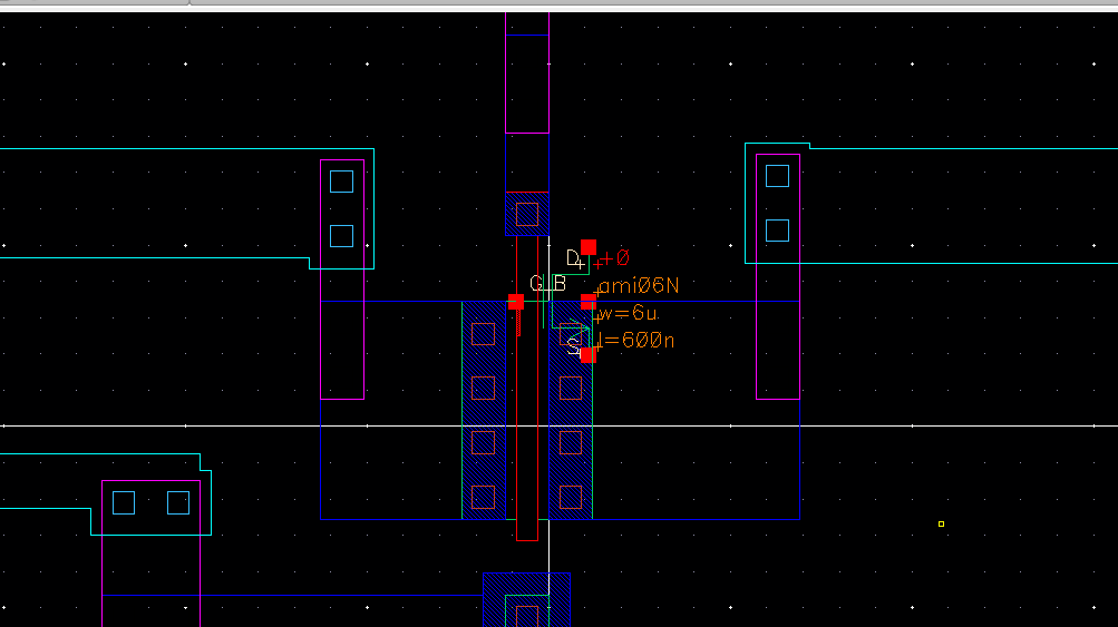
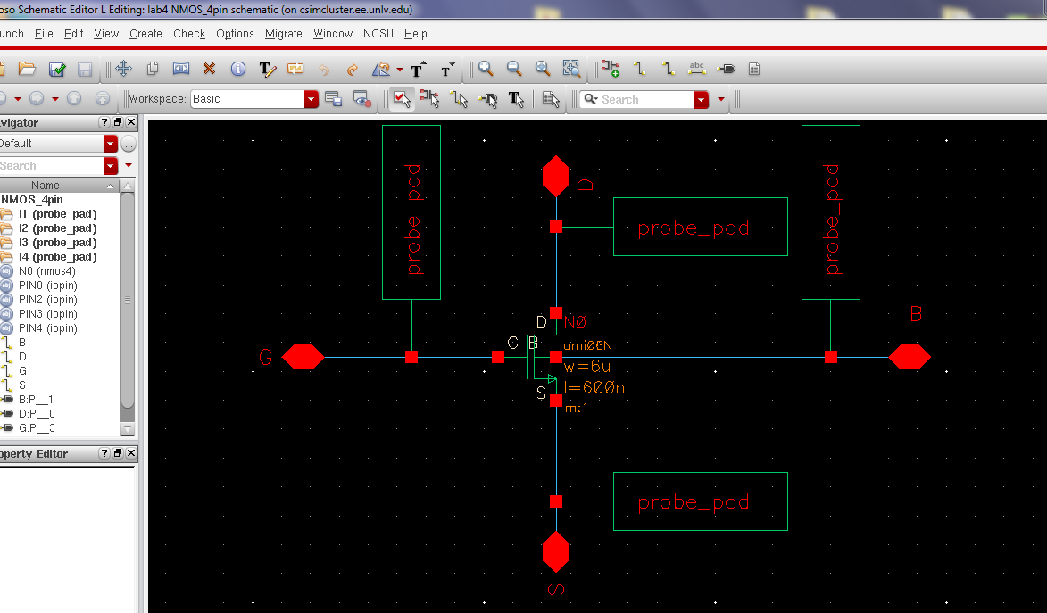
now
create a new schematic call NMOS_4pin and instantiate a 4pin NMOS from
the NCSU Analog Parts library and attach the probe pad to each of the
NMOS pin like below. make sure to change the width of the nmos to 6u
and Length to 600u.
now that both the schematic and the extracted is done we can LVS it to see if it has passed. and it did pass LVS. 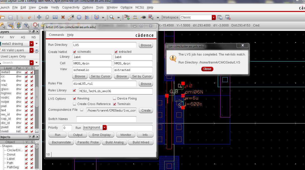
- Lay out a
12u/0.6u PMOS device and connect all 4 MOSFET terminals to probe
pads.
- Show your layout passes DRCs.
- Make a corresponding schematic so
you can LVS your layout.
now
create what we did for the nmos but instead now use a pmos. first
create a layout called PMOS_4pin. then instantiate a pmos from the
ami06 library, and set the dimension to 12u by 0.6u. instantiate a
m1_poly for the gate, and a ntap for the bulk. and add a pin for the
drain and source.
now add a m2_m1 to the 4 pins then add a m3_m2 as shown below.
lastly
add the probe pad like we did for the nmos and connect it with metal3
layer, and DRC yield zero error. and extracted the layout
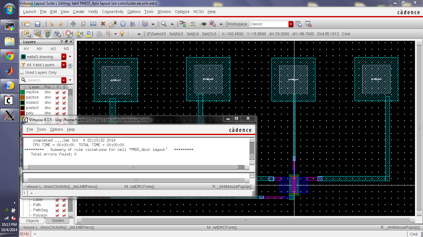
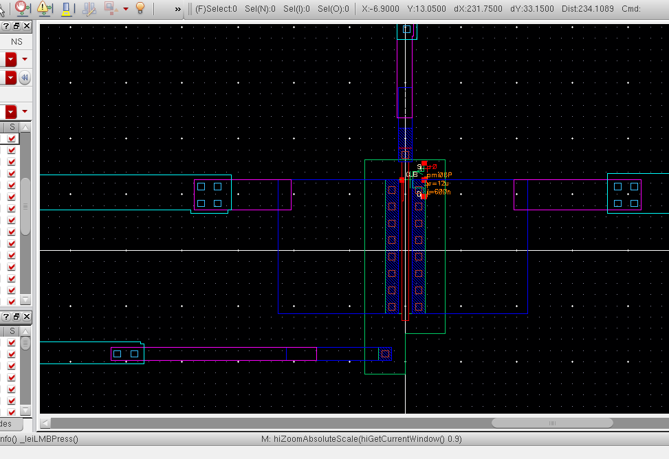
below is the zoom-in view of the extracted
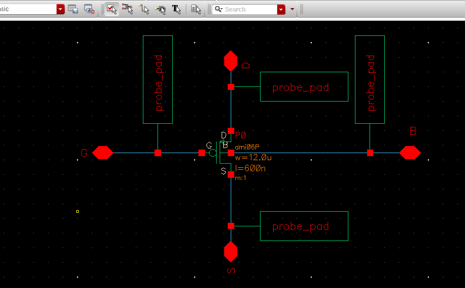
Next
we want to create a schematic of our pmos connected to the probe pad as
shown below. since both the nmos and pmos schematic is the same. copy
the schematic of the nmos and change the nmos4 to pmos4 from the NCSU
analog parts library.
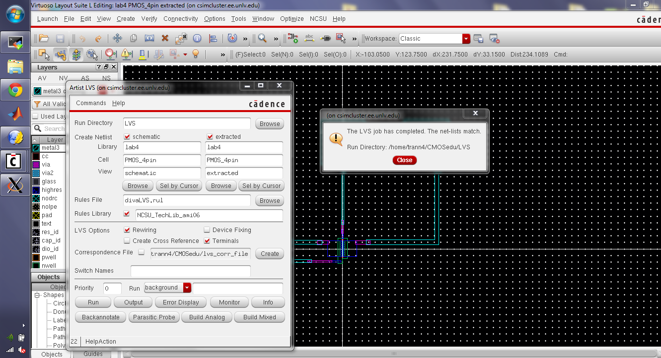
now
we want to see if our schematic matches our layout. we can do this by
LVS to check. open the extracted view of the PMOS_4pin and LVS it. the
netlist match indicate that LVS-sin was successful.
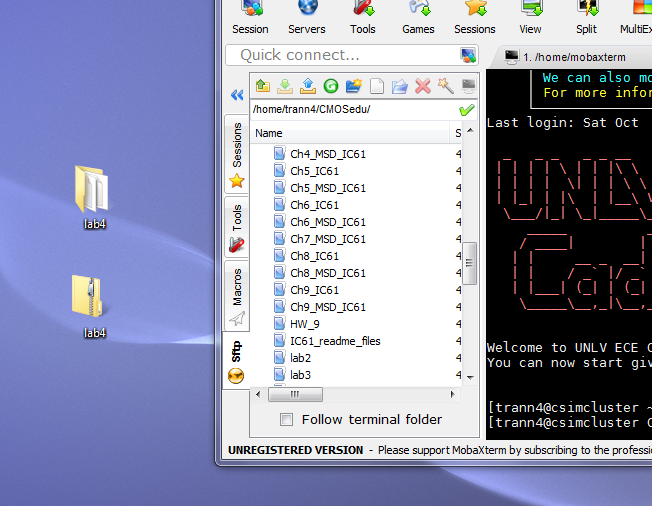
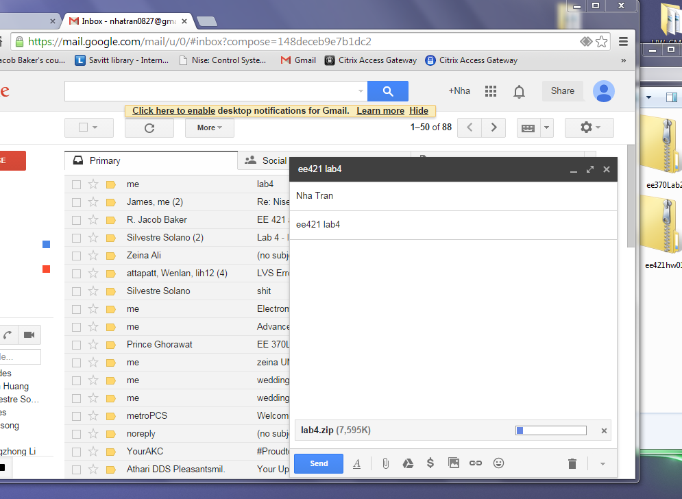
lastly
drag the lab4 folder from the MobaXterm to the desktop and zip it and
add a link to the lab4.htm. then email it to yourself.
lab4.zip
this ends lab4.
Return to EE 421L labs