Lab 3 - EE 421L
Authored
by Nha Tran
Email: trann4@unlv.nevada.edu
NHSE ID: 2000590233
09/24/2014
Lab objective: The purpose of this lab is to use the layour of the 10-bit DAC created in lab2 to make a 10k resistor
Prelab:
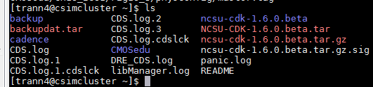
First create a backup of the work that was done previously in the class and lab by typing tar -cvf backupdate.tar CMOSedu/ in the MobXterm command line.
Next
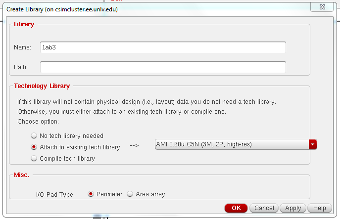
Open MobaXterm and run Virtuoso and create a new Library call Lab3, and
attached the tech library AMI 0.60u to the library.
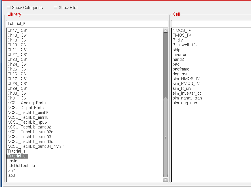
Next download the zip file Tutorial_6.zip from the cadence tutorial site located on the CMOSedu.comupload it onto MobaXterm in the CMOSedu folder. and Unzip the file. Type unzip Tutorial_6.zip in the command line in the CMOSedu folder.
After that is done you need to add its location in the cds.lib by typing DEFINE Tutorial_6 /home/trann4/CMOSedu/Tutorial_6now
check the cadence library manager and it should be located there (image
below). The Reason we want to upload tutorial 6 is because tutorial 6
has tutorial
1 through 6 on it so instead of having to upload them all we just need to upload tutorial 6 to get all the files we need.
LAB:
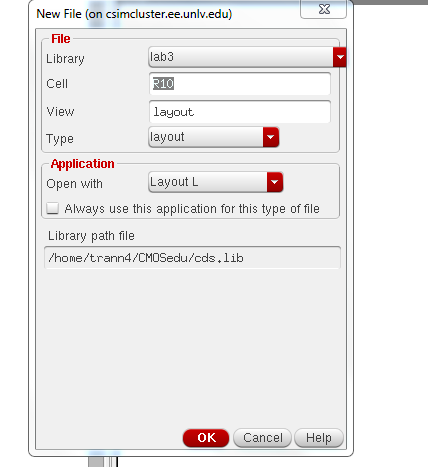
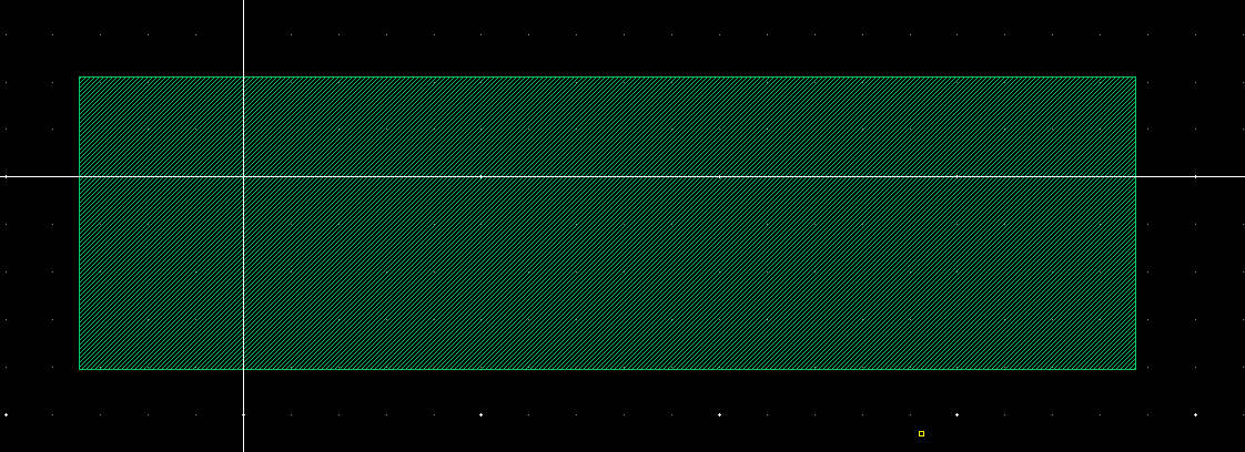
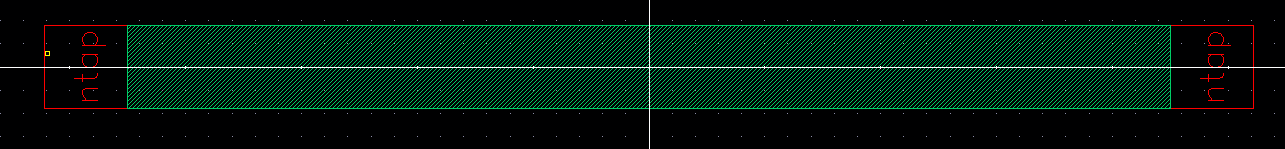
in this lab we will be using the n-well to create a 10k resistor. Create a new layout in lab3 by doing File --> New --> Cell View --> Layout
select the n-well layer and press the bindkey R to make a rectangle and draw something similar to below
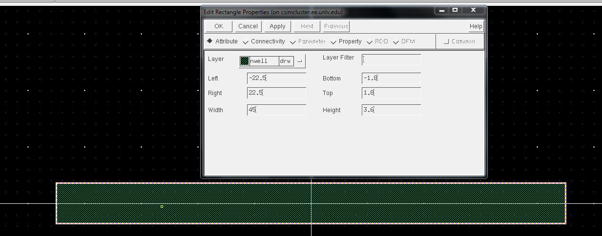
the sheet resistance in the C5 process is 800 ohm/square and we want our total resistance to be 10k so the equation is
Rtotal = Rsquare * (L/W)
10k = 800 ohm/square * (L/W)
L/W = 25/2
since
the C5 process required the l and w to be multiple of 3.6 (the minimum
width is 3.6) we have to multiply our top and bottom by 3.6/2 to get
L=45 and W=3.6. If we dont do the previous step and just draw a box
with 25L and 2W when we DRC it would give us an error. below is the
dimension of the nwell resistor
when DRC you see that the error is zero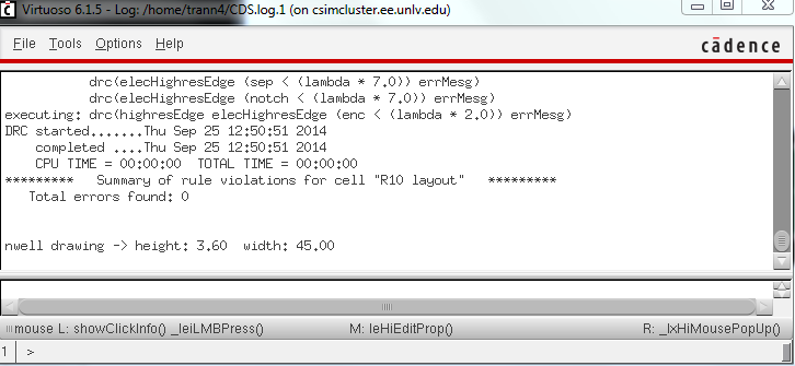
Next
we add the ntap layer to the end of the resistor to make the
connection. Press i to create an instance then Browse the
NCSU_TechLib_ami06 to find ntap layer and place 2 on the layout as seen
below 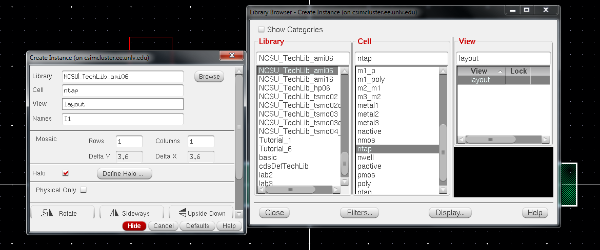
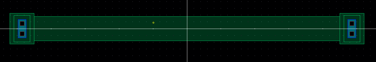
press e and change the stop to from 0 to 10
Next
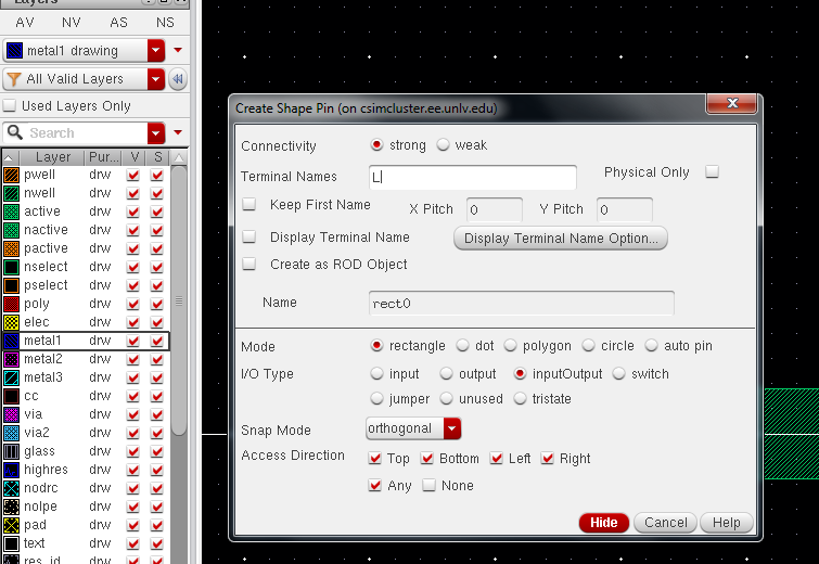
we will be adding pins to the layout select Metal1 layer and go to
Create --> Pins, name the terminal L and select display terminal
name. Do this for both the left and the right side.
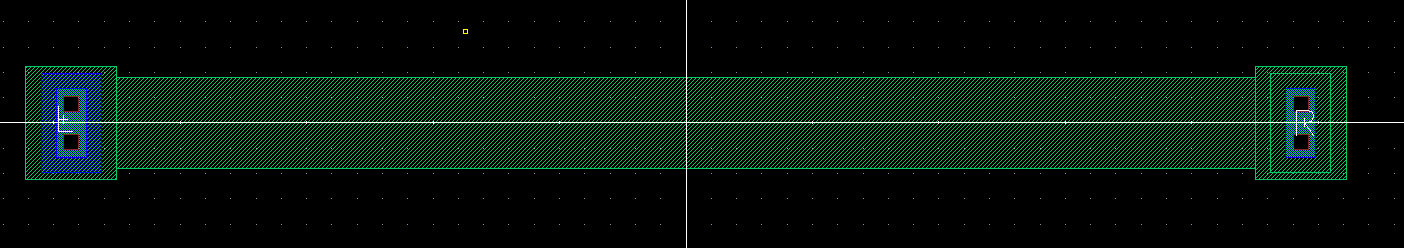
next
select the res_id layer and draw a rectangular box where the n-well is,
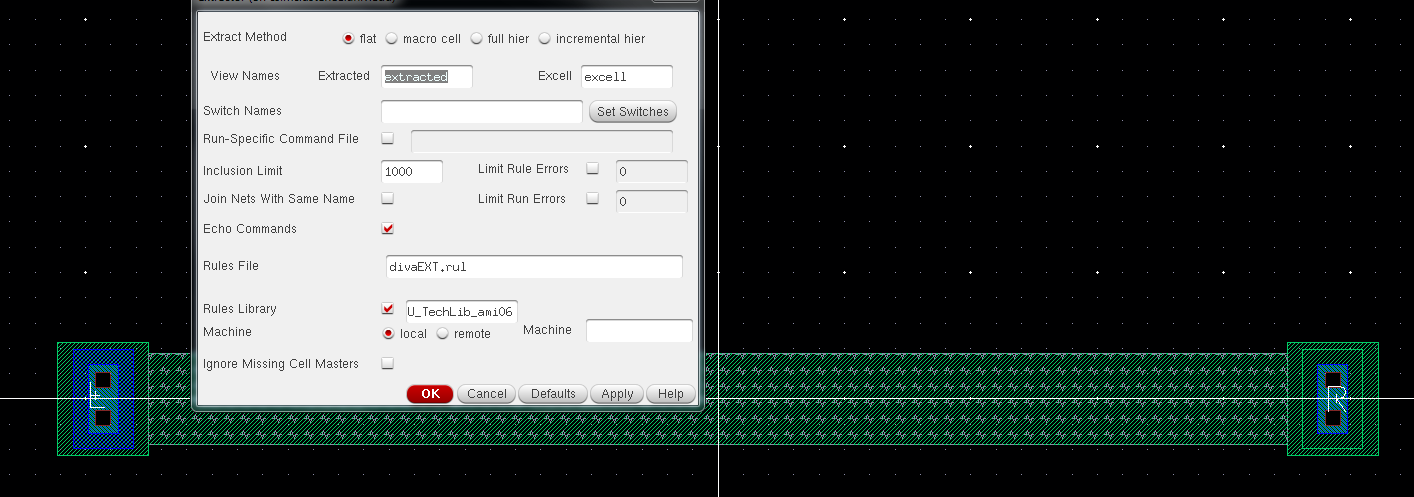
then extract the file by going to verify --> Extract
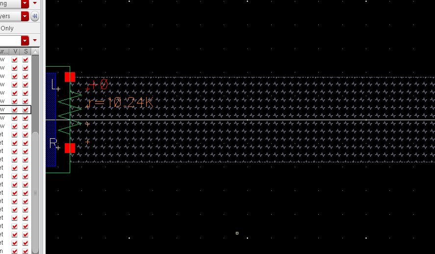
 Lastly the extracted n-well resistor value is 10.24k
Next
we want to make an 2R_R symbol using the n-well resistor that we just
created. Place 3 n-well resistor on the design window and layout it so
that it have the same x position but varying y-position. afterward
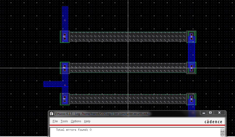
DRC-ing to make sure that it have zero error.
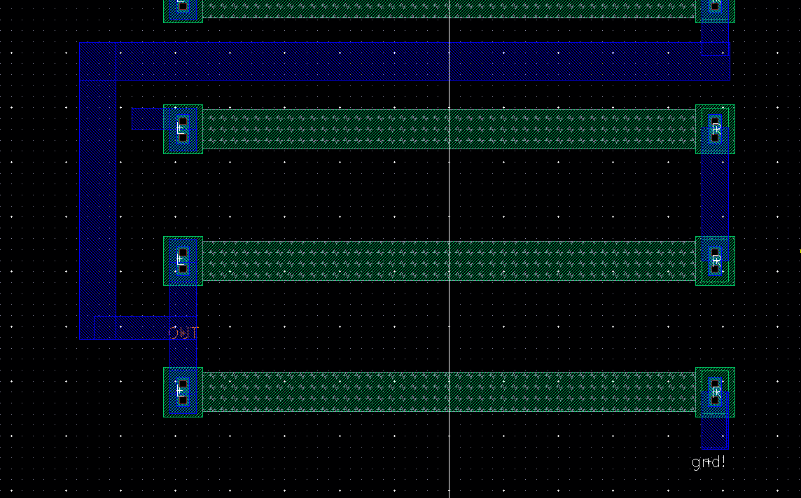
Save
the layout and create a new Layout so we can place 10 of the 2R_R in
parallel to create our 10-bit DAC. Each bottom pin of the 2R_R is
connected to the output of the one below it. The first 2R_R output is
connect to Vout and the last is connected to gnd!.
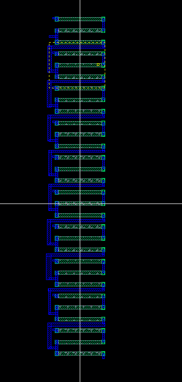
A
closer inspection of the lower part of the DAC you see that the bottom
is connected to a pin called gnd! which is the universal gnd.
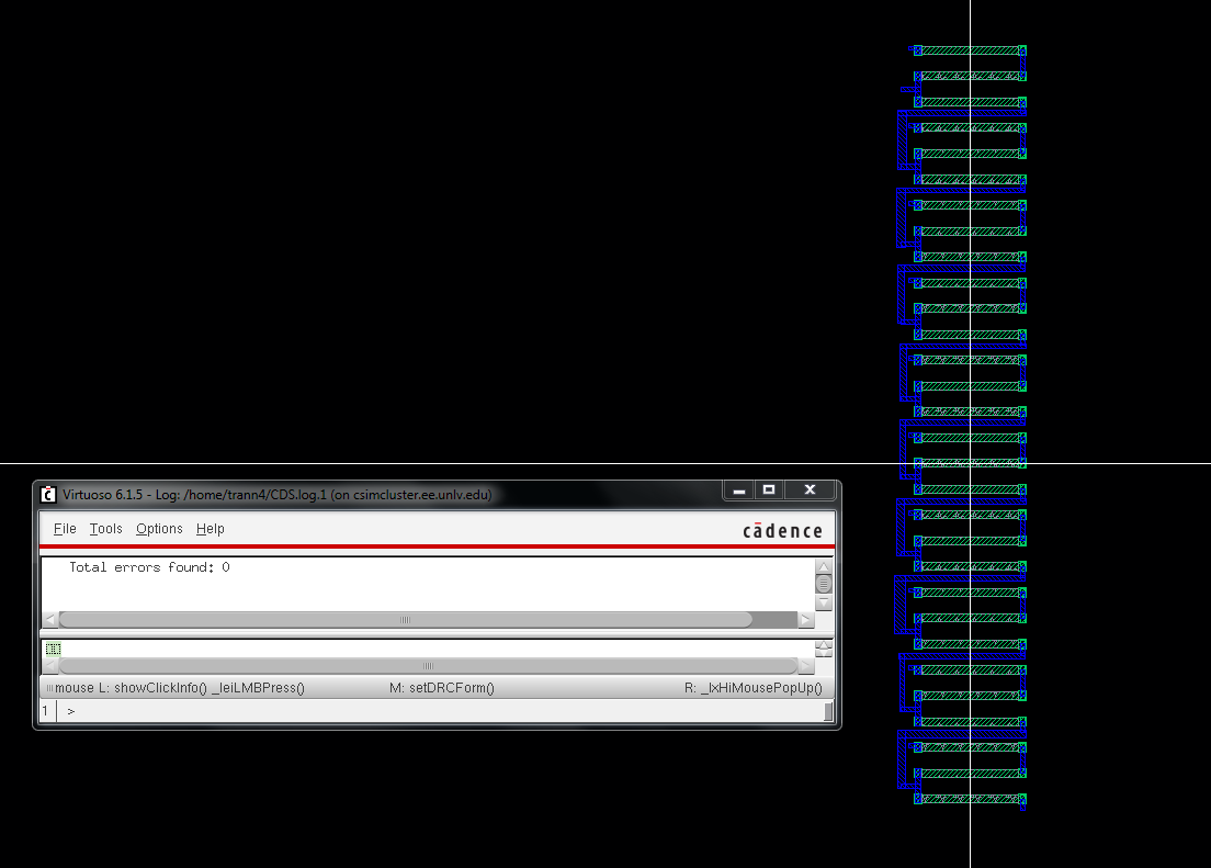
DRC-ing yield zero error.
when i extracted the layout to get ready for LVS looking at the resistor value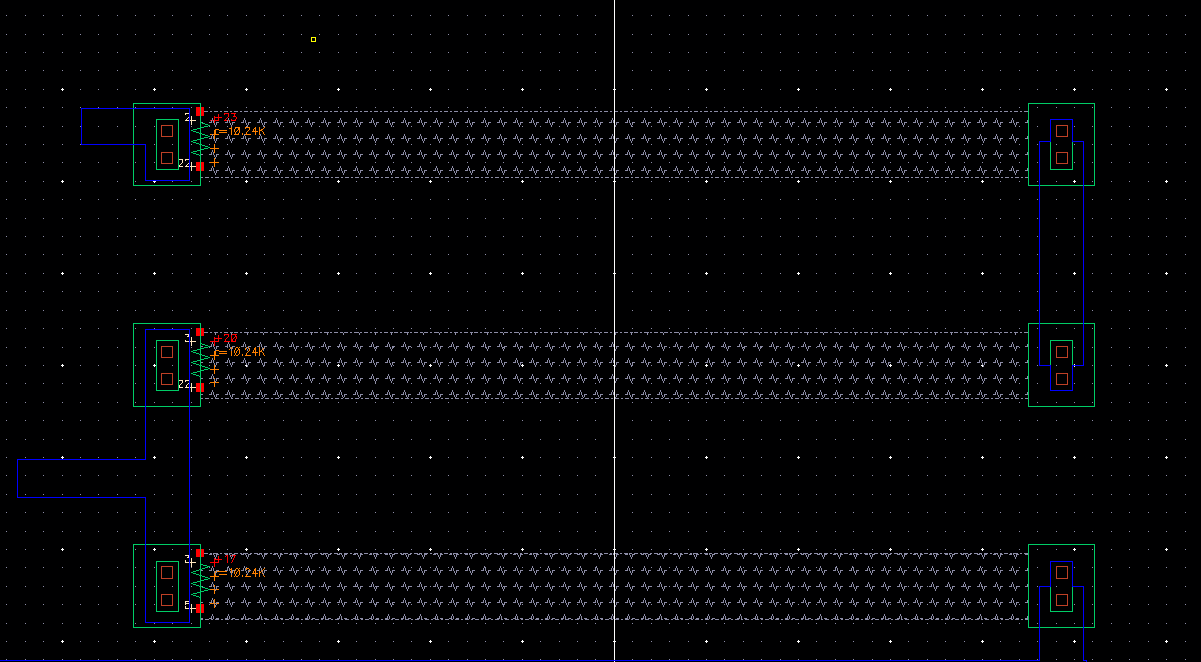
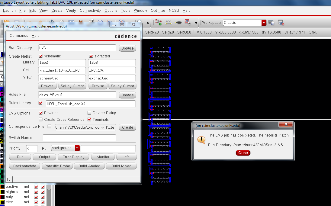
And finally LVS it and it matches the ideal 10-bit DAC from lab 2
Lastly zipping up lab3 folder and adding it to the lab3 html directory link and emailing it to myself for future reference
Return to EE 421L labs