Lab 2 - EE 421L
Authored
by Nha Tran
Email: trann4@unlv.nevada.edu
NHSE ID: 2000590233
09/15/2014
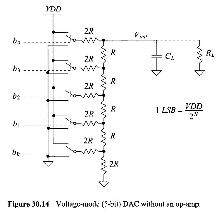
Lab objective: The purpose of this lab is to use n-well resistor to implement a 10-bit DAC.
Lab:
In
this Lab we will be using n-well resistor to recreate the topology seen
below. This Figure was taken from the CMOS book figure 30.14. We will
be creating each individual block and then connect each block to create
the 10-bit DAC.
1) Provide a narrative of the steps in the tutorial.
The first step is to download the lab2.zip file from the website and place it in the home directory. Unzip the file and add this "DEFINE lab2 $HOME/CMOSedu/lab2" to the cds.lib so the library can point to the right location.
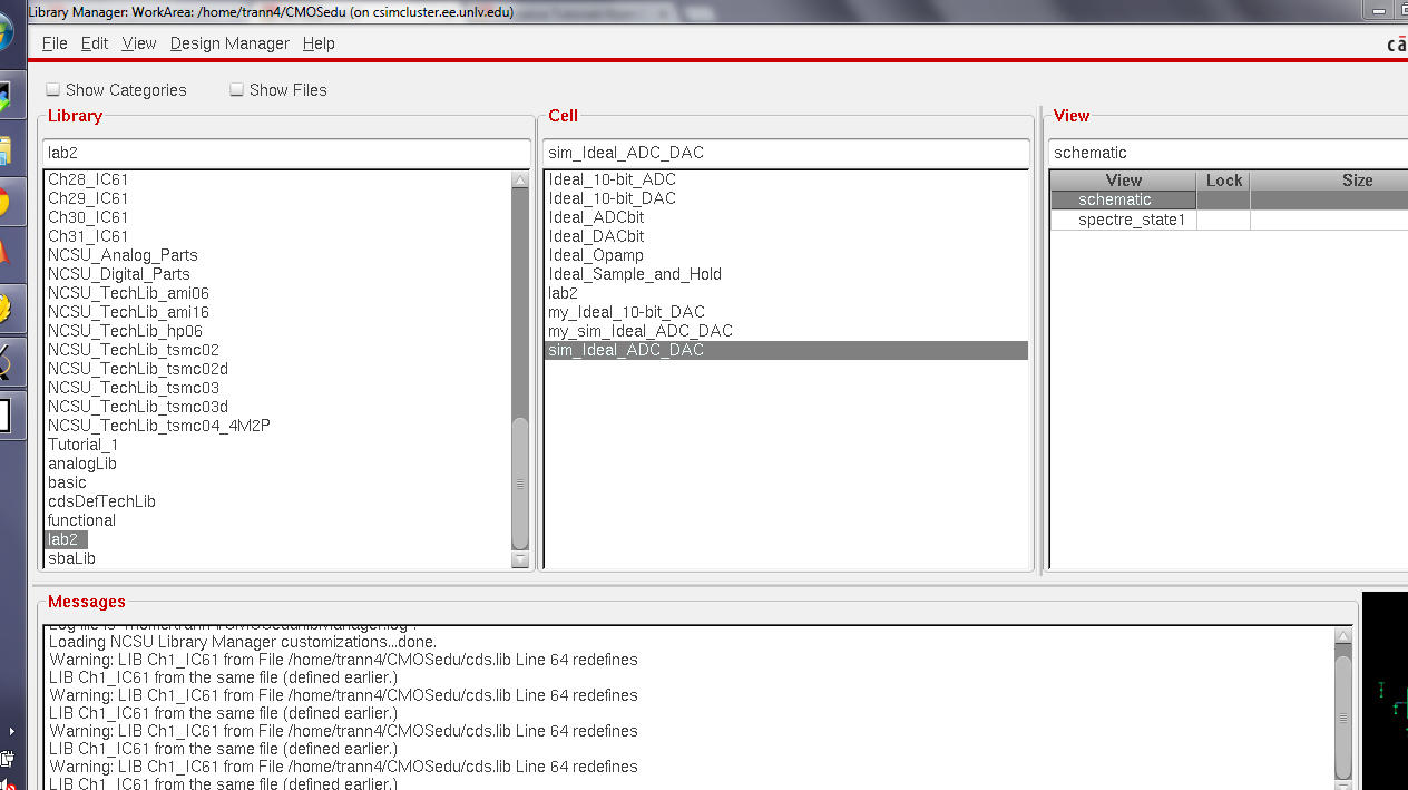
First open MobaXterm and run Cadence Virtuoso and it should appear like below
with a new library call lab2. Within this library select
sim_Ideal_ADC_DAC and view its schematic.
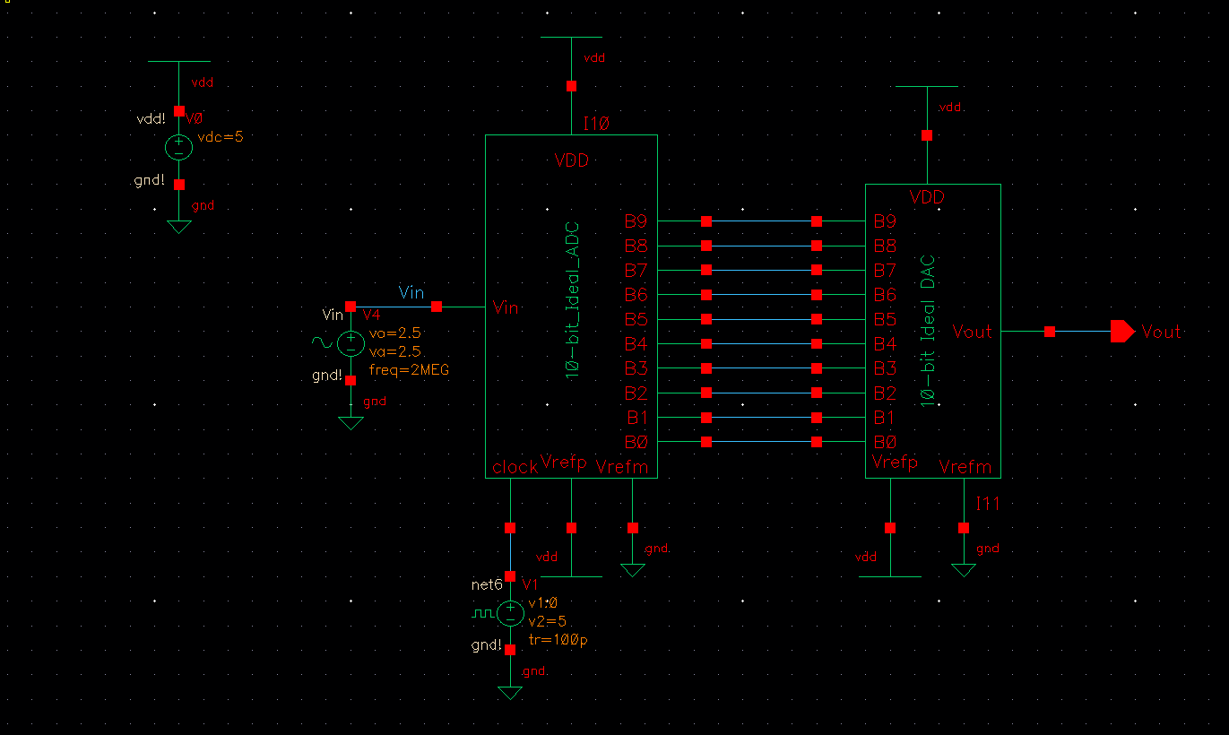
The schematic of sim_Ideal_ADC_DAC should look like the image below.
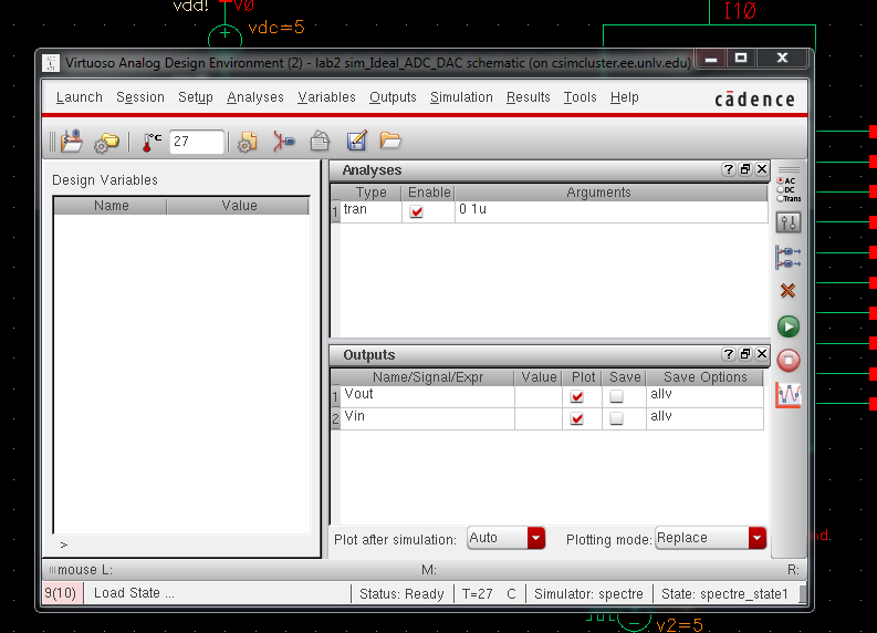
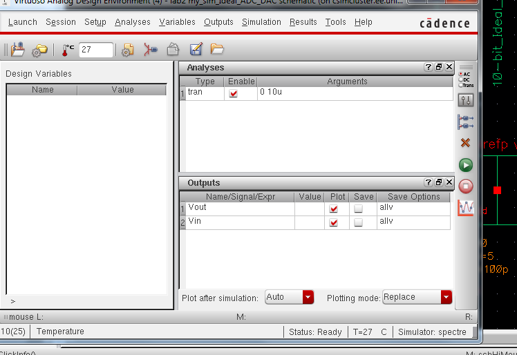
Running
ADE L --> Session --> Load State --> Cellview you should get a
screen that looks like the image below, notice that the analysis and
the output has already been choosen.
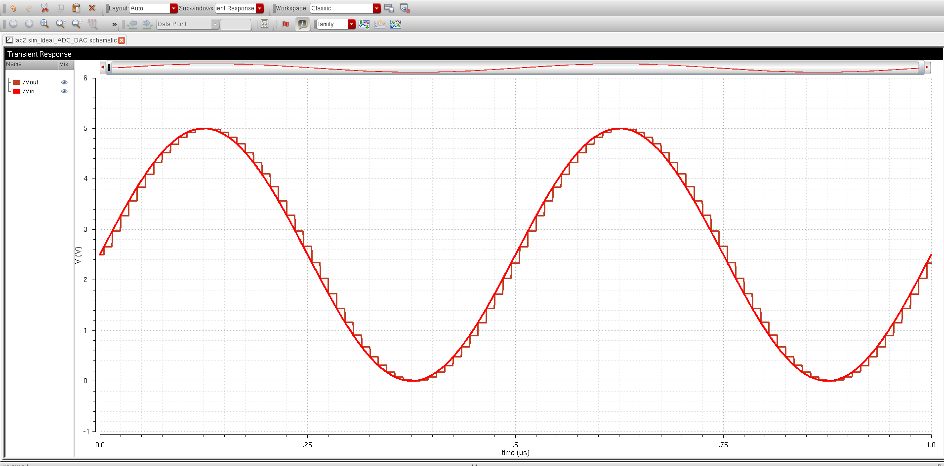
The
graph should look similar to the one below. With the Vout is the
triangle wave and Vin is the sinusoidal curve. I changed the background
to white and the Vin and Vout curve to thicker lines for better
visual presentation.
2) provide, and discuss, simulation
results different from the above to illustrate your understanding of the
ADC and DAC.
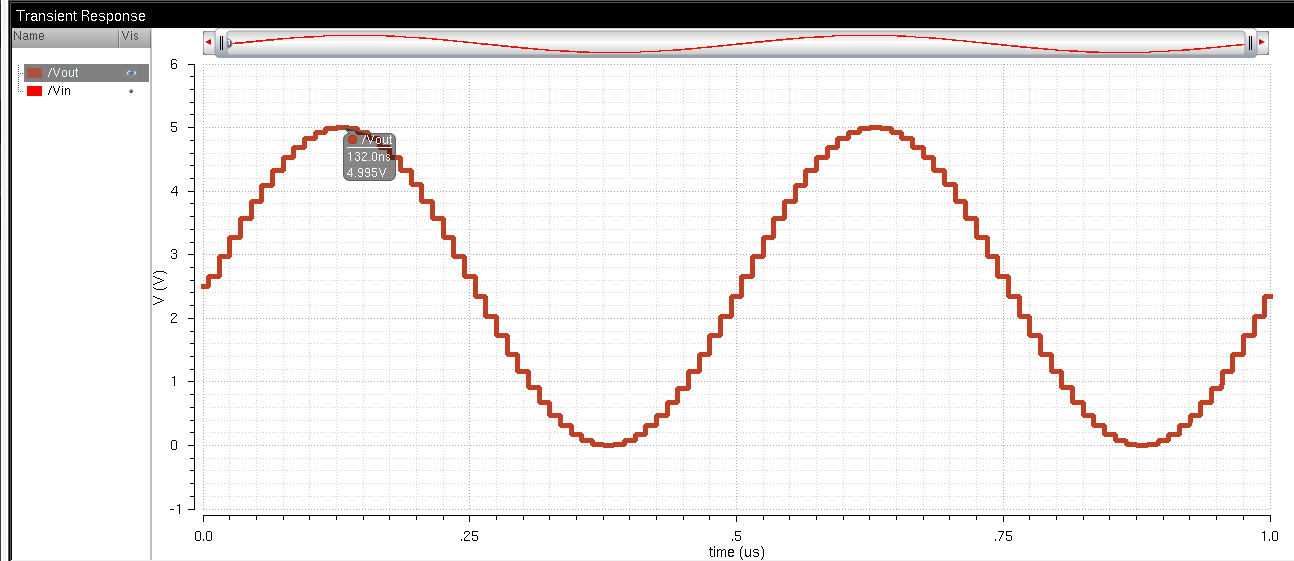
A
10-bit DAC has a 2^10 possible output. That is if the input is 00 0000
0001 or 1V then the output would be 1/(2^10) which is roughtly plus or
minus 1 mV than the input. Below you can see that the output is 4.995 V
this is because when Vin is 5 V, Vout will be only plus or minus 5mV.
3) Explain how you determine the least significant bit (LSB,
the minumum voltage change on the ADC's input to
see a change in the digital code B[9:0]) of the
converter
LSB
is determine by Vdd/2^n where n is the number of bits. for example if
the input is 0000 0001, and the VDD to ground is +5 V, then Vou/Vin
would be 5/(2^8) = 19.5mV, or if the input is 1000 0000 then Vout/Vin
would be 5/2^1 which is 2.5V.
Once we know that the
Digital-to-Analog Converter works its time to modify the DAC bus to
represent our own DAC design that was presented in the beginning of
this lab. The schematic stated at the beginning of the lab can be
drawn as is or we can break it up into individual blocks then
connecting them in series to form the desired schematic. This design is
better for us because it will allow us to make changes and modify the
schematic much easier if we have to, it will also make it less work
than having to draw the whole thing as is. As indicated and presented
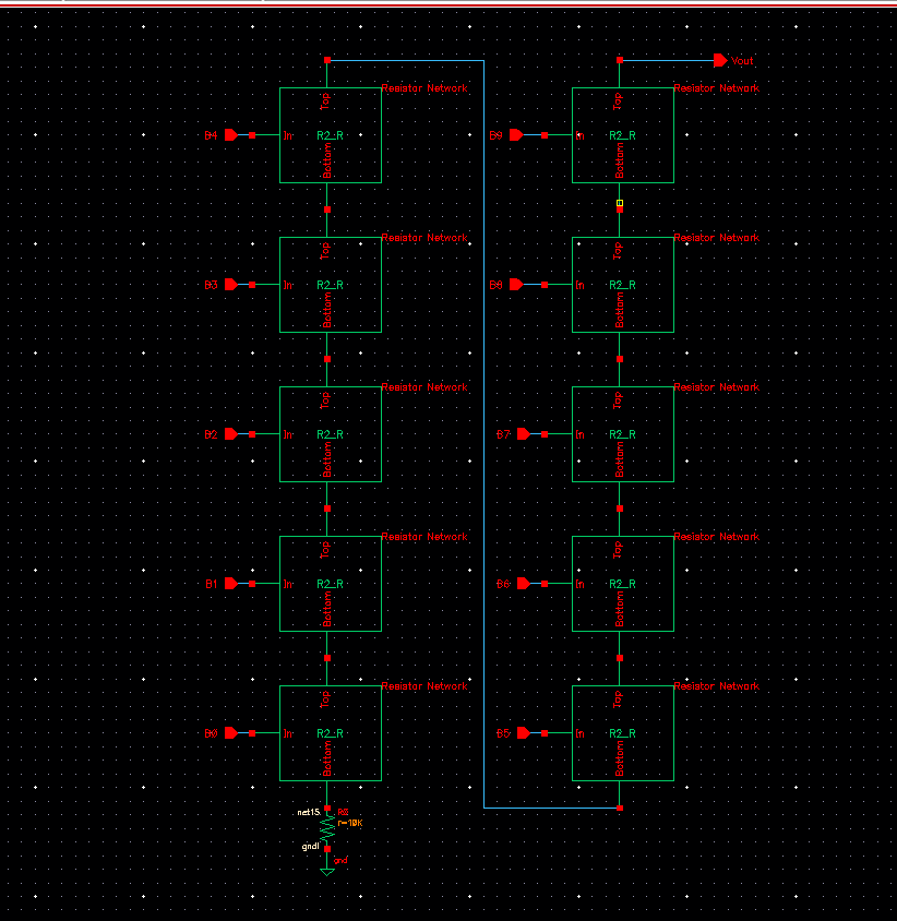
in the image below we broke the schematic into 10 different 2R-R.
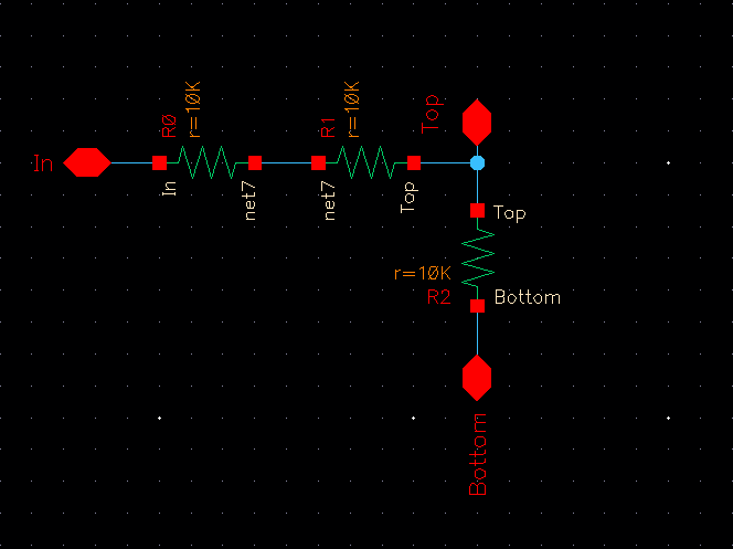
Below
is the symbol of the n-well resistor that will be used in the 10-bit
DAC. this symbol was created from the schematic above.
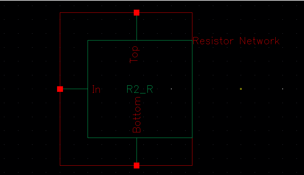
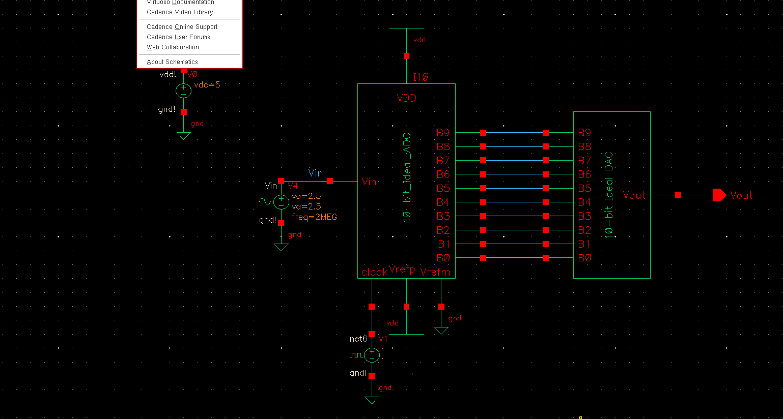
The
image below is the connection of the symbol created above. It is
connected in series from the premade ideal 10-bit DAC and modified to
look similar to the one image below.
This
image below shows the bus-connection of the ideal 10-bit DAC that was
created using the 2R-R resistor (image above). The ideal 10-bit DAC top
view is the one below, if you use bind-key x to go to the bottom layer
it would look like the image above.
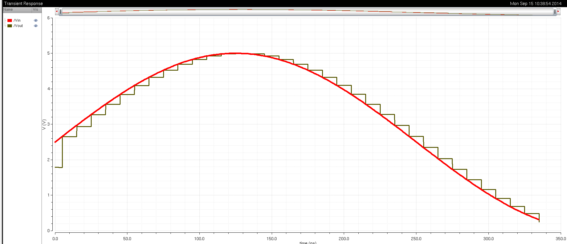
Running
the simulation you should get the image below with the input as the
smooth curve and the output is the jagged curve. The input is the
analog signal while its output is the digital signal, hence the term
Digital-to-Analog Converter.
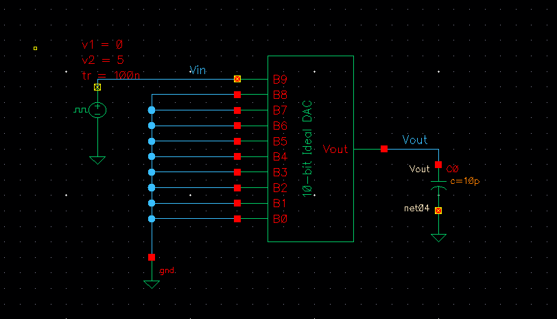
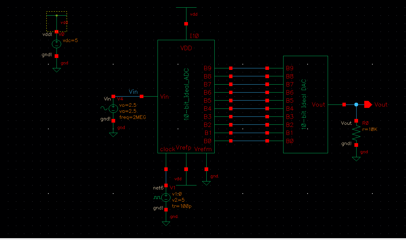
Next
we would like to determine the output resistance of the circuit that we
created. First copy the my ideal 10-bit DAC as new schematic. Than
connecting bus 0-8 to ground and bus9 to a 0-5V pulse and also connnect
the output to a 10pF cap. (image below)
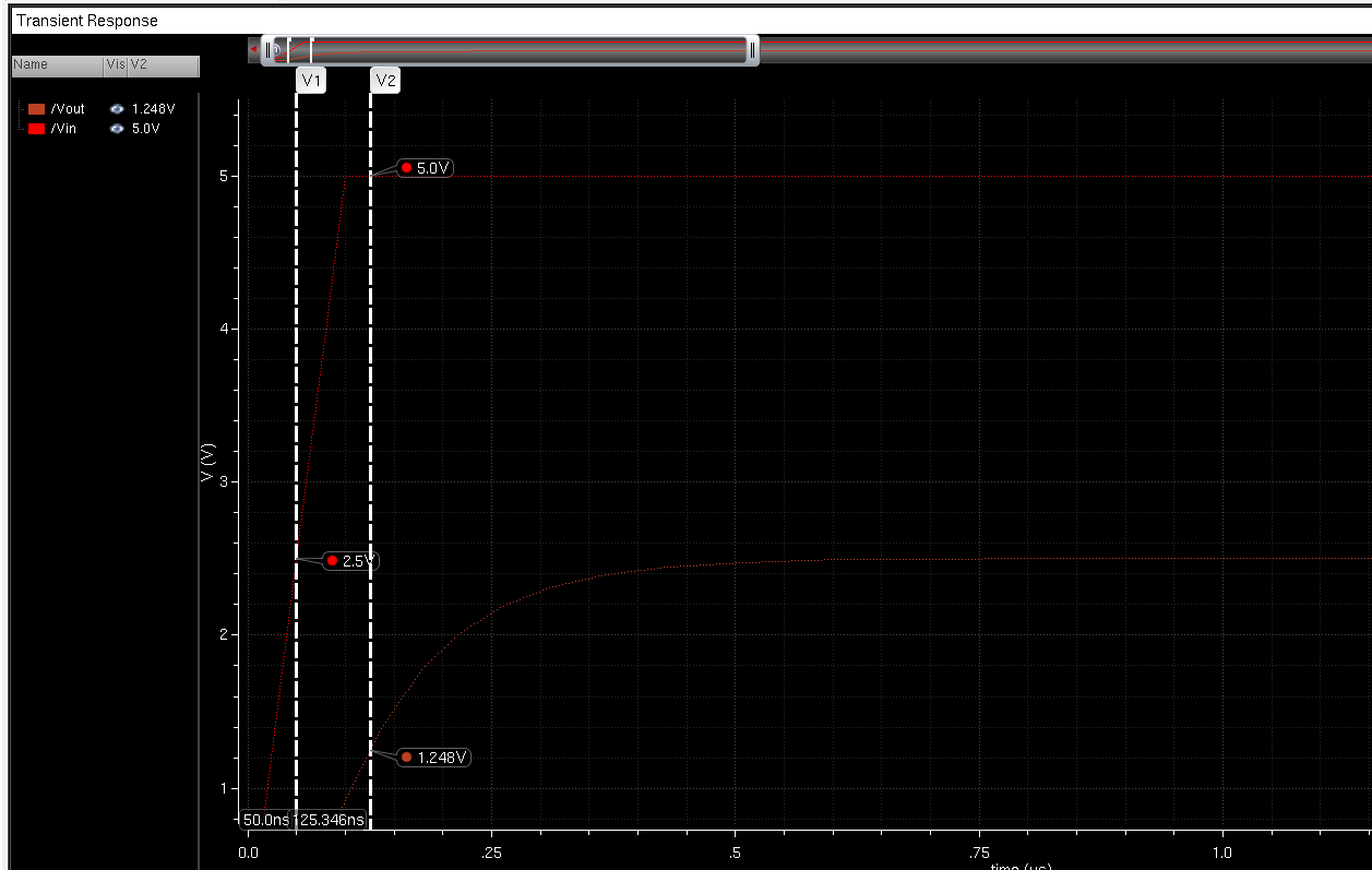
running
the simulation and setting the transient time to 5 micro seconds we
should get a graph similar to the one below and selecting the Vout and
VIn to be ploted (image below). Then we want to see if the delay time
is correct. we can use the equation time delay(Td) =0.7RC to estimate
theTd , to check if our result is correct we will place 2 markers on
the graph one at 5V and one at 2.5V. From the calculation Td = 0.7 *
10000 * 10e-11 = 70ns
when
zooming into the graph and checking the time delay when the output is
half of the input we see that 125-50ns = 75ns which is roughtly our
estimate of 70ns for the time delay from the calculation, therefore we
know that the circuit works.
Seeing
that our design works and our time delay is correct next we would like
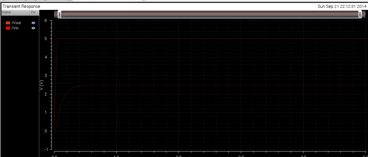
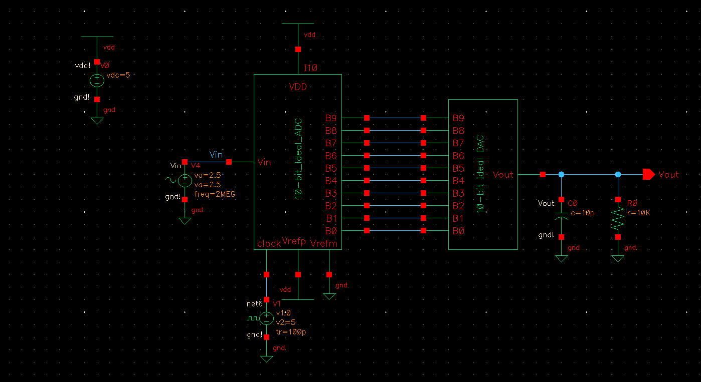
to see what happen when we drive a 10k Resistor into the circuit.
We can do this by adding a 10k resistor in parallel to the Vout
of our original ideal 10bit DAC converter. by adding the 10k Resistor
in parallel to the Vout we are creating a voltage divider and since our
total resistance for the ideal 10-bit DAC is 10k we see that the output
is now half of the imput. which we can clearly see on the graph
below.
when
placing a 10k resistor in parallel to the output the input is now half
which shows that the ideal 10-bit DAC has a resistance of 10k.
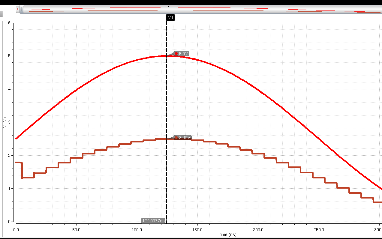
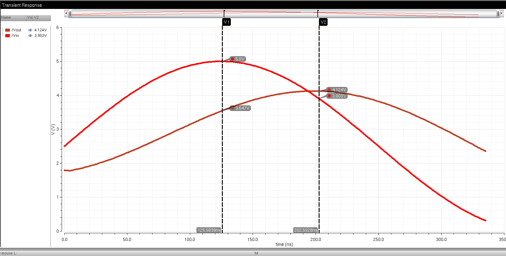
Next
we will add a 10pF cap to our circuit. Adding a capacitor to the
circuit will make the output be delayed and decrease its amplitude. the
capacitor charges and discharges with the increase and decrease signals
respectively. As seen below the capacitor also makes the curve much
smoother then previous circuit. We can also calculate its time delay
similar to the way we did in the previous steps above. as seen on the
graph the time delay is still around 75ns,. this is because we have not
changed the value of our capacitor.
Selecting
the marker to place peak-to-peak of each signal we clearly see that the
time delay is 75ns and also the amplitude of the output signal has been
decrease.
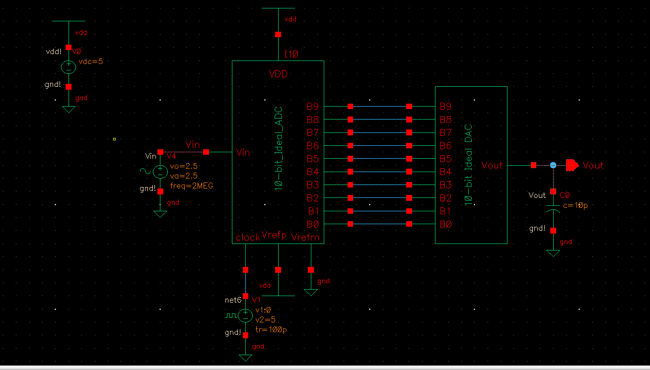
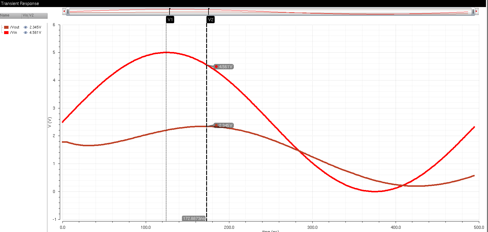
lastly we will be adding a RC in parallel to the circuit. Image below.
Again choosing to do a transient analysis with a 10 micro sec with the output and input to be plotted.
in
order to correct the convergence problem with cadence we have to set
the following paramater to make it converges which can be seen in the
image below.
- relative tolerance, reltol, of 10% (= 1e-1)
- voltage absolute tolerance, vabstol, of 100 mV (= 1e-1)
- current absolute tolerance, iabstol, of 1 mA (= 1e-3)
with this setup we can clearly see that both the amplitude and the time delay changes.
In a real circuit the switches
seen above (the outputs of the ADC) are implemented with transistors
(MOSFETs). If the resistance of the switch isnt small compare to R,
then input resistance of the DAC will be less than that of the switch
which will cause the current to go in the other direction.
Return to EE 421L labs