Project - EE 421L
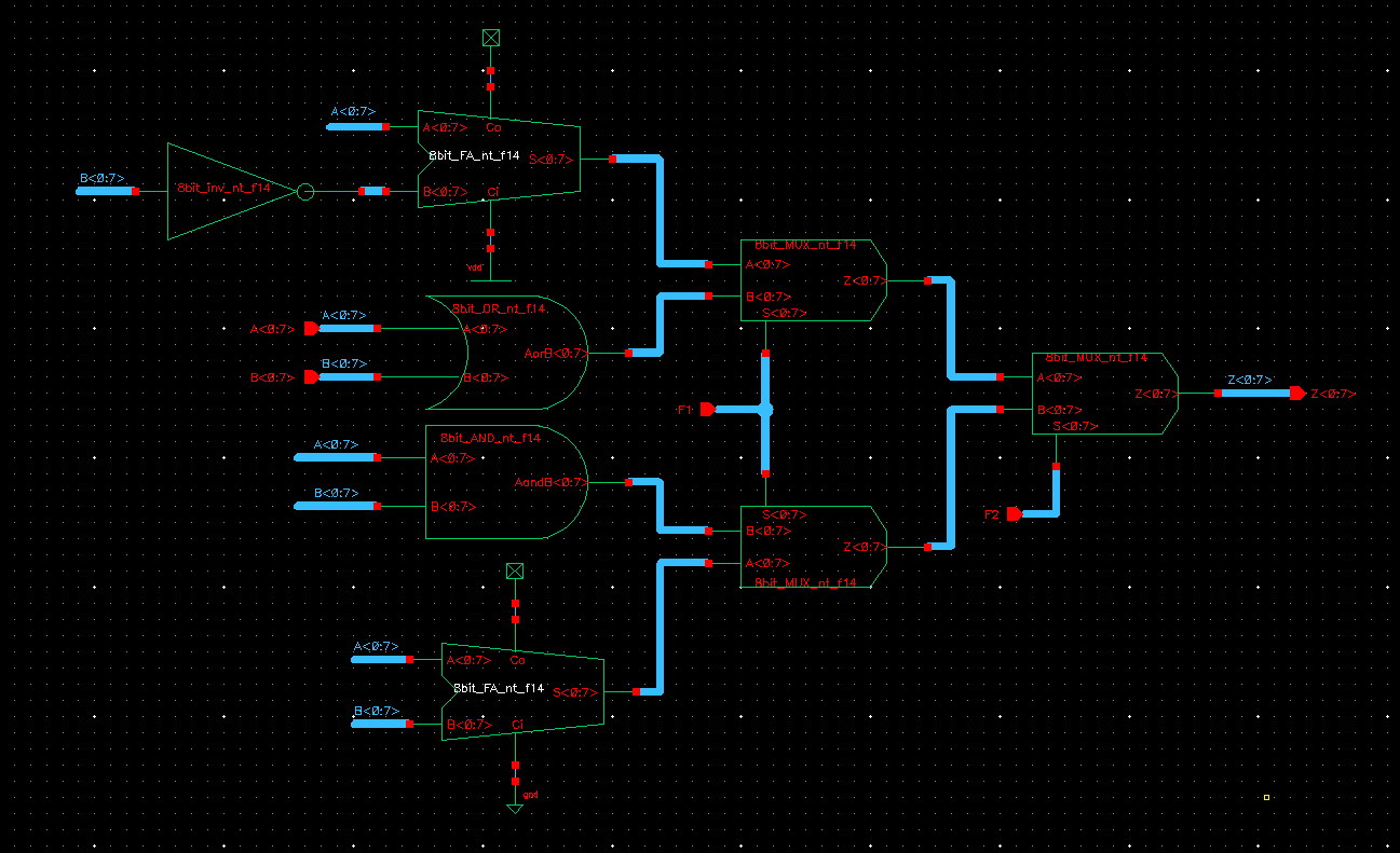
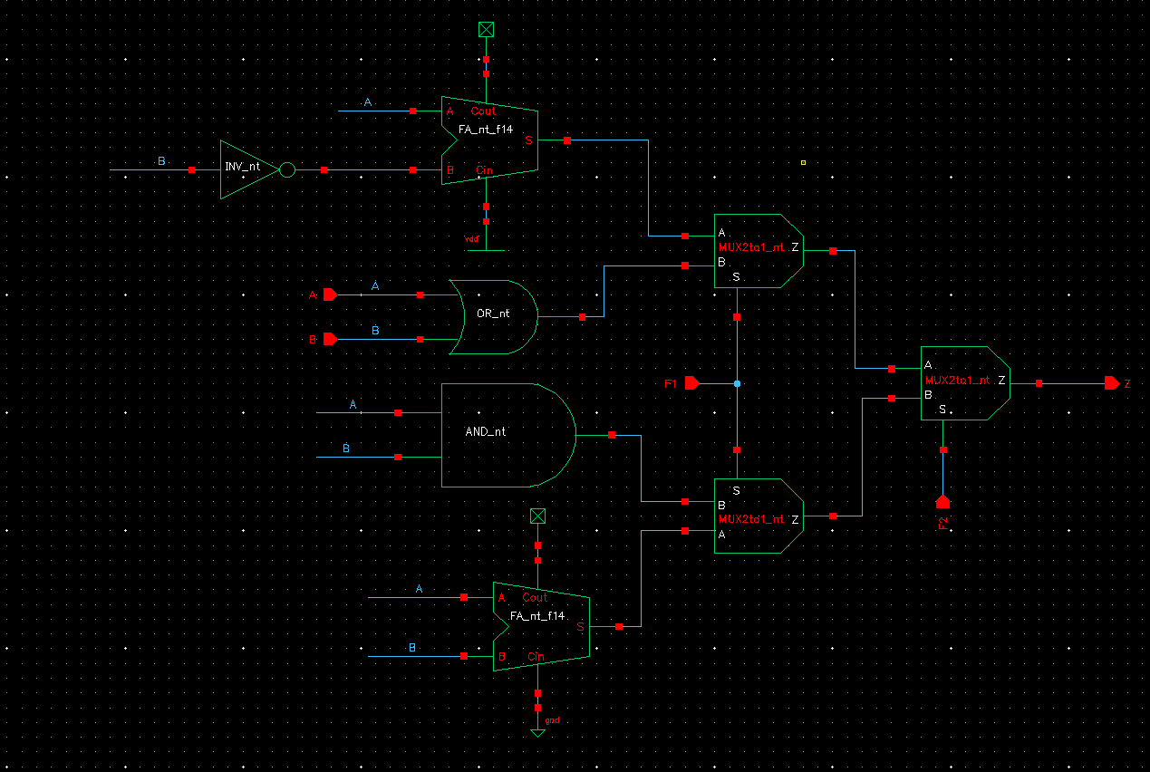
I start with a basic requirement for the project which is designing an ALU that can perform AND, OR, add, and subtract. Reading the gates from bottom up you can see that i place a Full-Adder(FA), AND, OR, and a FA with a inverter attached to B input. Next, all the output will go to two 2to1MUX that will select either a 1 or 0, and both of those MUXes will go to another 2to1MUX that will perfrom the same operation.
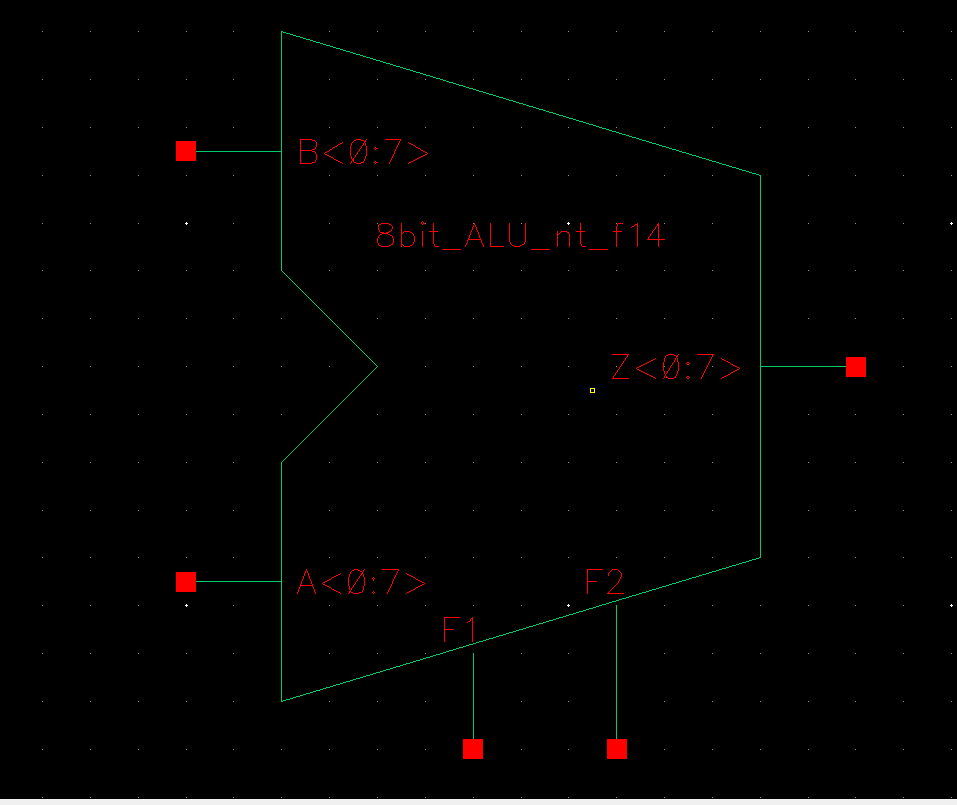
| F1F2 | |
| AND | 00 |
| OR | 01 |
| add | 10 |
| subtract | 11 |
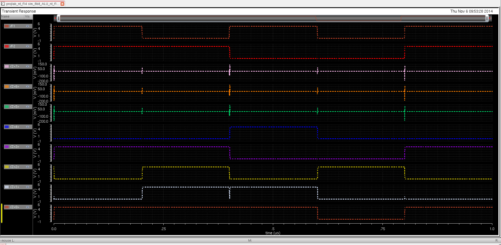
for testing the function of the ALU i inputted a 5V pulse for F1 and F2 with different period, my A is 0000 1110, and B is 0000 0101
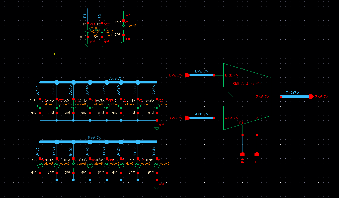
the result of my input A and B should be as followed
| Operation | Output (Z) | |
| 00 | A AND B | 0000 0100 |
| 01 | A OR B | 0000 1111 |
| 10 | A + B | 0001 0011 |
| 11 | A - B | 0000 1001 |
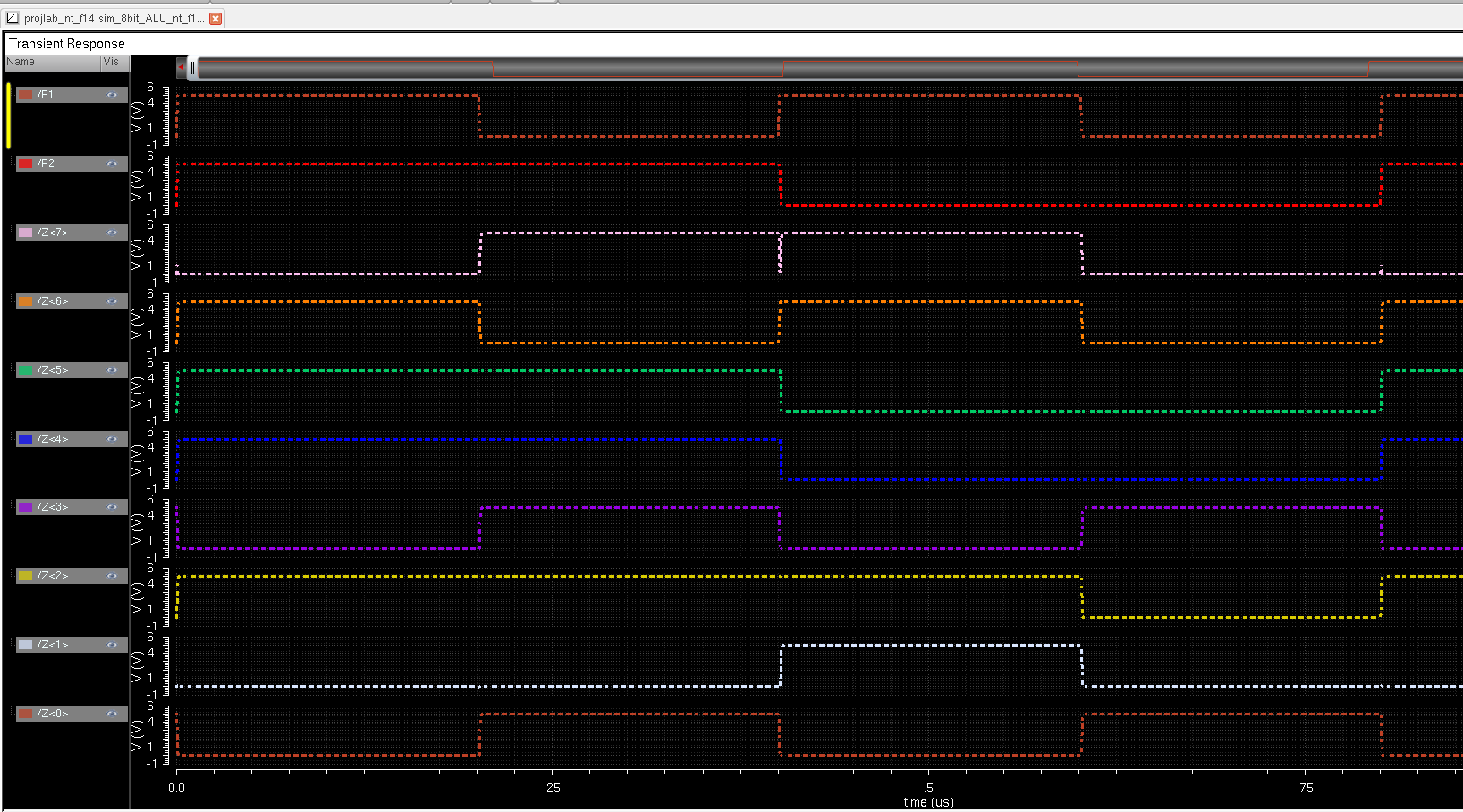
However for sanity check i will use a different input to see if it works for all values of A and B. this time however A will be 1001 1101 and B will be 0110 1001. The output should be as followed.
| Operation | Z | |
| 00 | A AND B | 0000 1001 |
| 01 | A OR B | 1011 1101 |
| 10 | A + B | 1100 0110 |
| 11 | A - B | 0111 0100 |
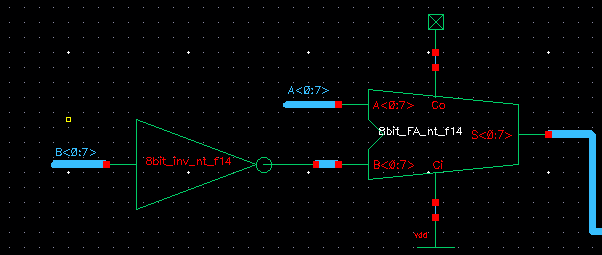
The schematic of the AND, OR, FA, and MUX was designed in previous labs so i will not go into details of it or how it works. The only one that was not covered in previous labs is the subtractor using a FA. Below is the image of a subtractor. Its operation is simple to understand, because the CPU cannot understand subtraction the way a human brain can, we have to program it to do subtraction via 2s-complement. 2s-complement is easy to understand with no deep thought, if we have A-B, all we need to do is invert B and add 1, then add to A. As you can see from below. B is inverted and Ci is a constant vdd which is 1. The addition of A + B-inverse + vdd(1) will give you A-B. The Cout is left as a No-Connection in this case because we are only doing A-B where B<A. However we can adjust it easily if we want, in case where B>A, then the Cout will be 0 which indicate that is it a negative number, and when B<A Cout will be 1 which is a positive number.
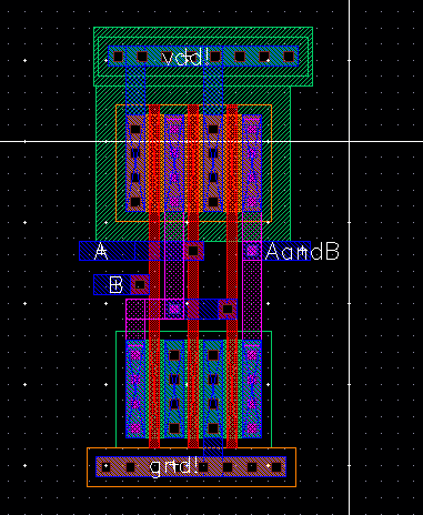
Next i will start laying out each individual elements in the ALU then make a 1 bit ALU. Note that in previous labs the schematic of the element was drafted but not the layout. First up is the layout of a AND gate.
Next is the layout of the OR gate.
Next up is the 2to1MUX
Lastly is the FA which i made in previous lab but it was too messy so i adjusted some metal to make it cleaner
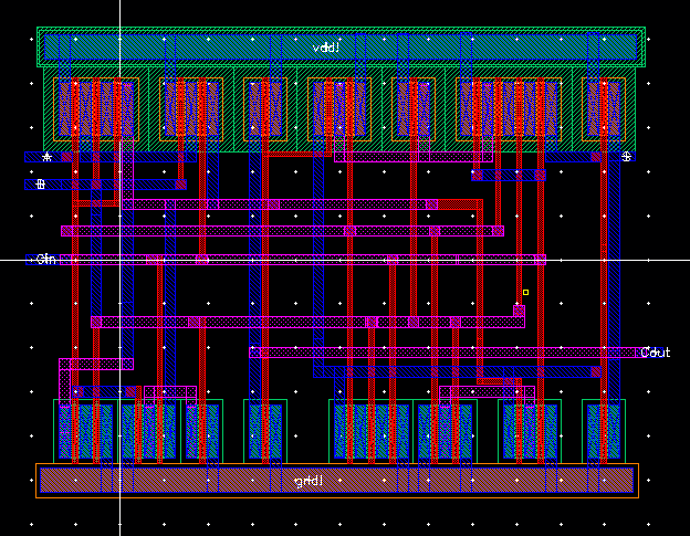
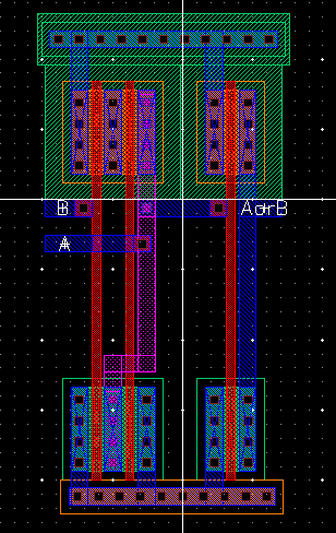
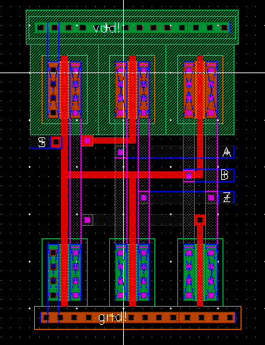
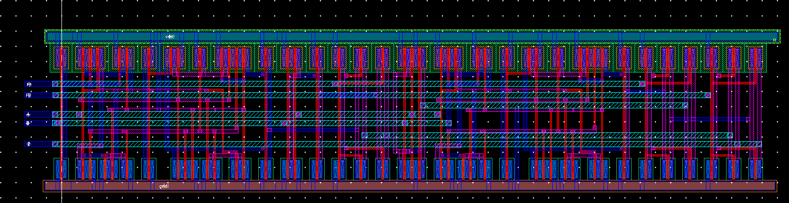
I made my ALU to mirror my schematic reading from top to bottom. The left most of my ALU is the subtractor, then the OR gate, and both connected to the MUX. Next is the AND gate then the FA both of which is connected to the second MUX, then the two previous MUX will connect to a third MUX. As seen below in the layout. I did a stretch of all the layout of the AND, OR, INV, and MUX to match the height of my FA. At first, my idea was to make all the vertical connection on metal2 and all horizontal connection on metal1 that way it would look cleaner. but somewhere along the process i just mix them up.
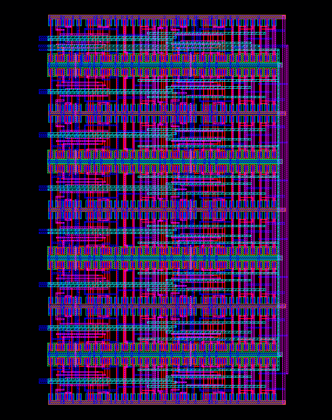
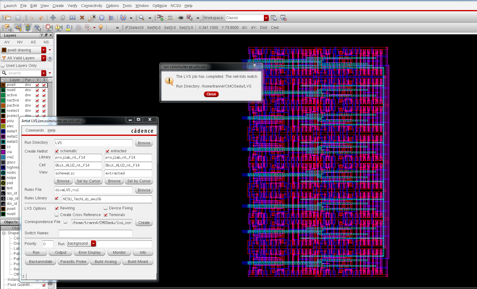
below is the image that it LVS
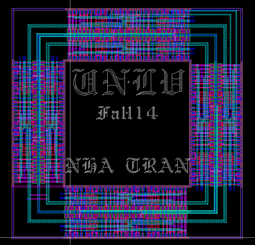
The above layout was actually my second layout, my first layout (image below) is aesthetically better but functionally not so good because there is a big gap in the middle which i put my name and UNLV in it to fill up the gap. But for grading purposethe first one should be graded not the one below. The one below can be use as reference for future students taking Dr. Baker's design class for what not to do.
Lastly, zipping up the design folder and emailing it to myself as a backup.