Project - EE 421L
Braxon Tawatao
tawataob@unlv.nevada.edu
11/22/2014
Project - Part 1:
Schematic of the 8-bit ALU with 26 pins - In1(8), In2(8), S(2), Out(8):

For this ALU the 2 select bits can be used to choose an operation as follows:
| S1 | S0 | Operation |
| 0 | 0 | In1 AND In2 |
| 0 | 1 | In1 OR In2 |
| 1 | 0 | In1 + In2 |
| 1 | 1 | In1 - In2 |
Corresponding symbol:

The ALU was simulated using the following schematic:

Simulation of AND operation:

This
simulation illustrates 1111 1111 ANDed with 0000 001. The highlighted
outputs are all logic 0 while Out<0> is a logic 1.
Simulation of OR operation:

This
simulation illustrates 1000 0000 ORed with 0000 001. All of the highlighted
outputs are logic 0 while Out<0> and Out<7> are logic 1.
Simulation of 127 + 1 = 128 (unsigned in binary):

The result is 1000 0000 as expected. This demonstrates that carry of each FA functions correctly.
Simulation of 255 + 255 which causes an overflow and results in 1111 1110:

Simulation of 0 - (-1) = 0 + 1 = 1 (unsigned in binary):

Only Out<0> is a logic 1 which is expected.
Simulation of -128 - 1 = -129 (which is an overflow) or 128 - 1 = 127 (unsigned in binary):

The highlighted outputs are all logic 1 while Out<7> is a logic 0.
Backup of current project files:

The Part 1 of the Project design directory can be found here.
Project - Part 2:
After re-evaluating my previous design, I realized that the use of 3 full-adders was quite inefficient.
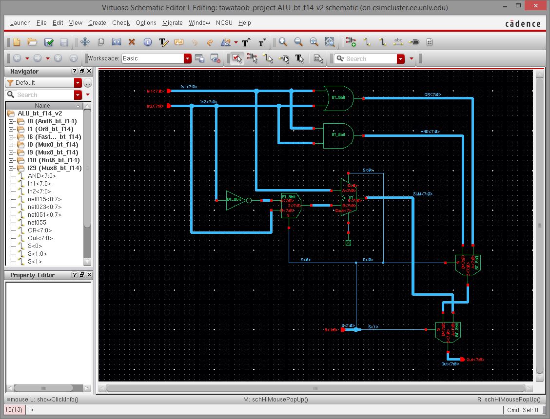
I re-designed my 8-bit ALU to be the following circuit. This is version 2 of the 8-bit ALU:
Schematic:
Symbol:

However, rather than creating a single layout for the entire ALU schematic, the ALU layout can be more efficiently completed by
instead
laying out a 1-bit ALU then cascading 8 of these blocks to create the
8-bit ALU layout. The final design was done in this way.
This is version 3 of the ALU:
1-bit ALU schematic:

1-bit symbol:

Layout of the 1-bit ALU:

Layout passes DRC:

Layout passes LVS:

Using the 1-bit ALU, an 8-bit ALU can be made:
8-bit Schematic:

8-bit Symbol:

Layout of the 8-bit ALU. Layout also passes LVS:

Layout passes DRC:

Backup of project files:

The entire Project design directory can be found here.
The cells that have "v3" appended to their titles consist of the final design.
Return to labs