Lab 7 - EE 421L
Braxon Tawatao
tawataob@unlv.nevada.edu
10/26/2014
Pre lab:
Building the 4-bit inverter from Tutorial 5:

And the resulting waveforms:

The
inverter is inherently resistive, and any capacitance attached to the
output will cause an RC delay where the time-constant is given by 0.7RC.
Therefore,
out0 has very little delay as there was no capacitor connected to it.
From out3 to out1 the delay becomes progressively better as
the capacitive loads diminish.
Lab:
Five 8-bit gates were created. These were NOT (inverter), NOR, NAND, OR, and AND. In order to create the AND and OR gates,
an inverter was simply used in conjunction with the previously built NAND and NOR gates.
The 8-bit gates were simulated using a single schematic:

Two bits (bit <1> and bit <4>) from each 8-bit output were selected and given different capactive loads.
The results from simulating are as follows:

Slight glitches occur in some of the gates, but the overall logic of each gate functions correctly.
Next, the operation of the single bit Mux/DeMux is shown.
Schematics of Mux/DeMux, respectively:


Simulation waveforms of each, respectively:

When the select is high, input A is routed to the output, and when it is low, B is routed to the output.

In the DeMux, when S is high, the input is output to A, and when S is low, the input is output to B.
The 8-bit Mux/DeMux, operates similarly to its 1-bit counterpart:
Schematics:


Waveforms:


For
the simulation of the 8-bit Mux/DeMux, capacitors were placed on the
outputs to show further simulations of delays and also to differentiate
between specific bits of the 8-bit bus lines.
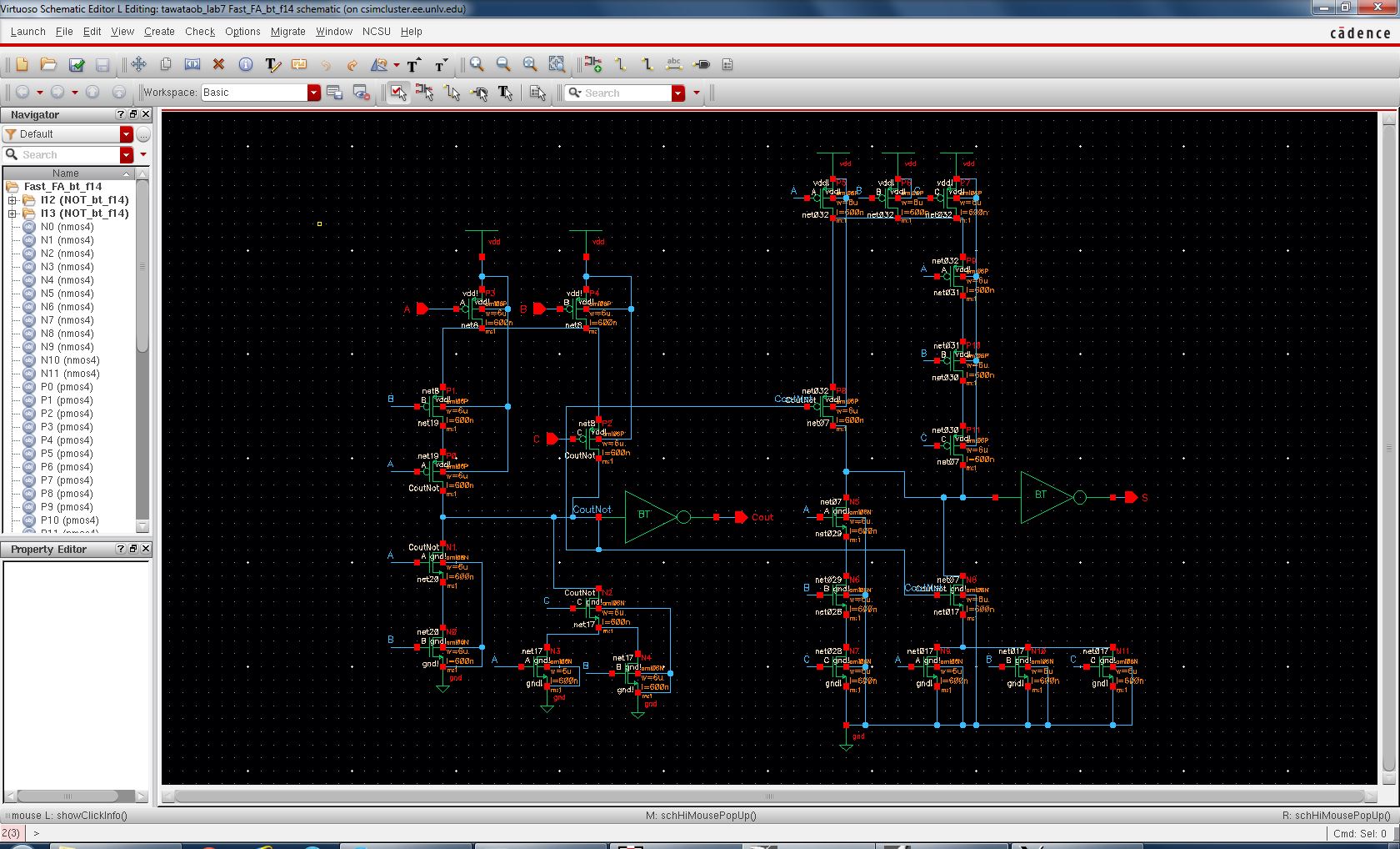
Lastly, the fast full adder based on Figure 12.20 was built (schematic, symbol, and layout).
1-bit Full adder schematic:
Symbol:

Layout (DRC and LVS):

By using 8 of these 1-bit FAs in cascade, an 8-bit full adder can be built and simulated.
Schematic:

Symbol:

Layout (LVS passes):

Simulation of the 8-bit adder:
Schematic:

Results of simulation:

To
show that this full adder works, binary codes 1111 1111 and 0000 0001
were added. To accomplish this, 5V was connected to every
bit of
input, A, and 0V was connected to bits <7:1> of input, B while 5V
was connected to B<0>. The sum of these inputs is shown to be: 1
0000 0000.
Cout<7> = 5V while all 8 bits of the output, S, are
0V. This combination of inputs succinctly illustrates the operation of
the 8-bit full-adder.
In adding these 2 specific binary numbers,
every carry from each individual full-adder must be utilized. However,
any other valid combination
of binary values will also sum correctly.
Lab 7 Backup:

The Lab 7 design directory can be found here.
Return to labs