Here is the circuit schematic for a NAND gate:

From the above schematic a NAND gate symbol was created:

And here is the layout for the NAND gate (DRC and LVS):


The inverter or NOT gate that was built in Lab 5 was also used in this lab.
Here are cells of the NOT gate (schematic, symbol, and layout):


Next a XOR gate was created, and the NOT gate from the previous was used here.
Schematic:

Symbol:

Layout:

Using the previously built gates, a digital 2-bit full-adder was made in the following schematic:

Symbol:

Layout:

Simulations:
Now that the various components have been built, we can simulate the operation of each.
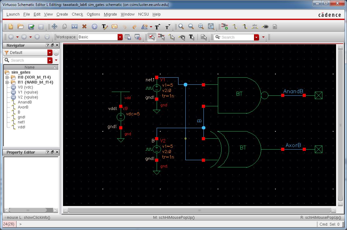
This is the circuit used to simulate the NAND and XOR gates with every possible combination of inputs:
The simulation results:

For the most part, the simulation ran as expected. However, there was a glitch in the output of the XOR gate. This was caused by the timing of the change in the inputs.
Different sections of the circuit have differing delays throught their MOSFETs, and no input can change instantaneously. Therefore the outputs of a digital circuit
may experience variations that are very quickly rectifed once both the input pulse and entire circuit reach steady state.
This is the circuit used to simulate the operation of the full-adder with every 3-bit input combination:

Simulation results:

This simulations verifies that the full-adder generates the correct binary sum of any 3 digital inputs, and also shows that there are glitches on the cout line.
The glitches on cout are caused by the glitches in a XOR gate which were discussd in the previous simulation. Looking at the full-adder schematic, it can be seen that
only cout is dependent on XOR gates and that s is not. That is the reason why cout glitches and s does not.
Backup of Lab6:

The Lab 6 design directory can be found here.
Return to labs