Lab 5 - EE 421L
Braxon Tawatao
tawataob@unlv.nevada.edu
10/9/2014
Pre lab (Building schematics, layouts, and symbols):
Building a schmatic for an inverter circuit with MOSFET sizes of 12u/6u and a multiplier of 1:

The spice parameters of the NMOS and PMOS respectively:


Here is the symbol generated from and containing the m1 (multiplier=1) inverter schematic:

Constructing NMOS and PMOS layouts of 12u/6u inverter respectively:
Ptap is used for the body of the NMOS, and Ntap is used for the PMOS.

The layout parameters of the MOSFETs:


Metal1 and poly was used to connect the pieces of the layout together.
The pins in the inverter layout have also been placed, and the completed layout passes DRC:

The extracted layout and corresponding schematic also pass LVS:

Generally, the same design process was follwed to build the inverter of size 48u/24u and multiplier of 4.
Schematic and MOSFET circuit parameters:


Here is the symbol generated from and containing the m4 (multiplier=4) inverter schematic:

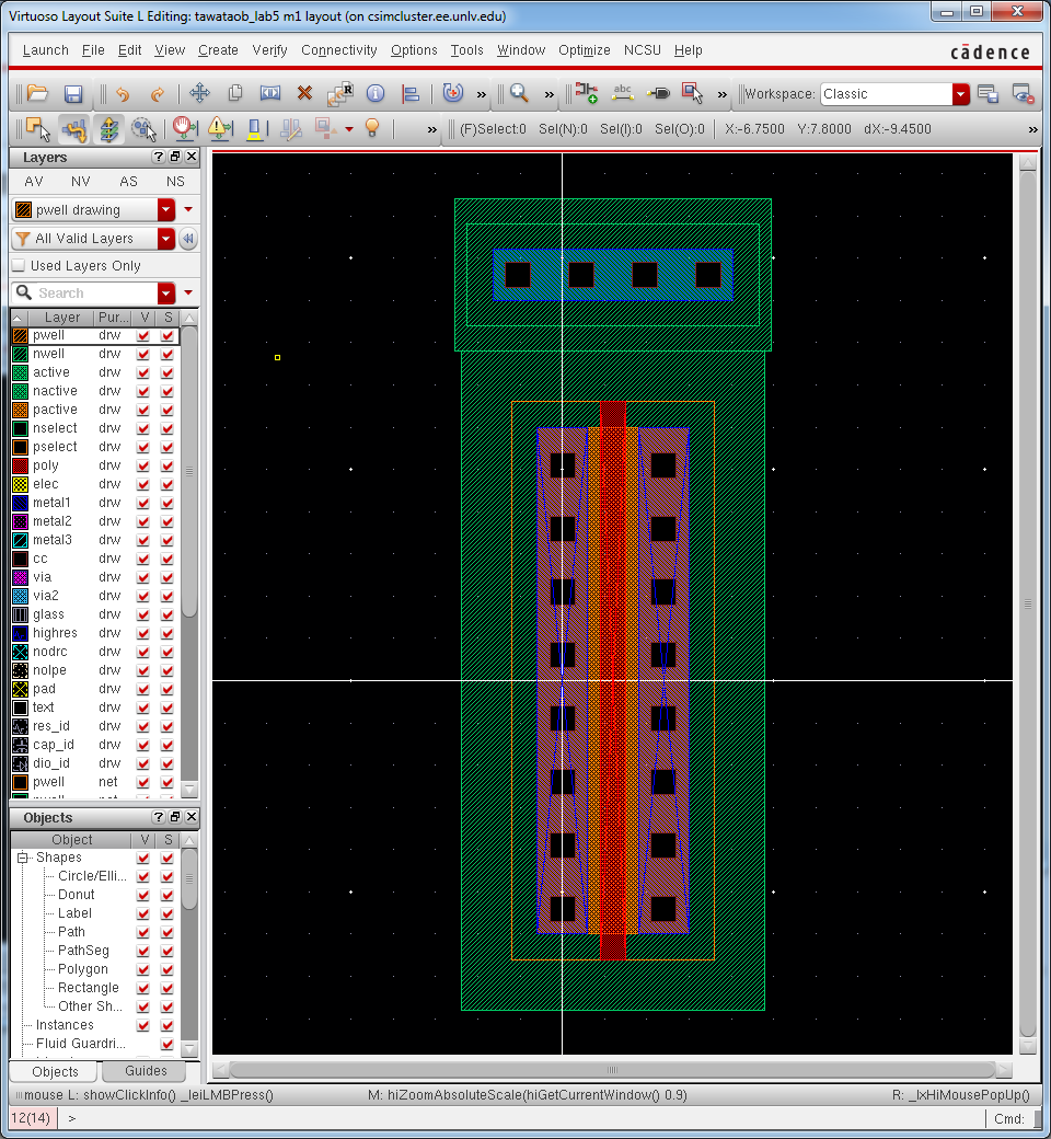
Laying out the larger inverter (the parameters of the NMOS and PMOS are shown below the layout):
Again, Ptap was used to connect to the body of the NMOS, and Ntap was used for the body of the PMOS.
Using 4 channels in parallel allows for an overall wider channel which lessens the resistance of the MOSFET as a whole.


A view of the final layout and DRC passes:

LVS of extracted layout and inverter schematic:

Lab (Simulations):
The general circuit used for all of the subsequent simulations is shown below.
Two differently sized inverters were used according to the simulation along with varying load capacitances.

Simulation of the first inverter schematic using spectre (multiplier = 1):
A parameteric sweep by decades was used for this simulation; the capactive load was varied between 100fF, 1pF, 10pF, and 100pF.
The input to the inverter is shown bolded.

Simulation of the second inverter schematic using spectre (multiplier = 4):
Again, a parametric sweep of the capacitive load was used, and the input is bolded.

The first simulation was run again, this time using UltraSim:

Then
the second simulation was run using UltraSim. A discussion of all of
the simulation results will be seen following this graph.

Discussion:
The
delay time constant of the circuit is given by RC, where R is the
output resistance of the inverter and C is given by the size of the
capacitive load.
For the first inverter in which the multiplier was
1, the delays were considerably longer than the delays given by
the inverter circuit whose MOSFETs had multipliers of 4.
The delays
from the first circuit were longer due to the large resistances of the
MOSFETs used for that inverter, if R is large then RC large.
On the
other hand, when the multiplier for the MOSFETs was 4, the channels of
the PMOS and NMOS were much wider causing an overall
decrease in the
resistance of the inverter. The 4 output traces for each simulation
represent differing output capacitances. As the capacitance
escalates
so does the delay. In fact, the delays for the 10pF and 100pF loads in
each simulation were so great that the output in both cases never fully
reaches 0V or gnd.
UltraSim did not seem to give
drastically different or less accurate results. However, the
simulations performed in this lab were not very large.
Even the spectre simulations completed quite quickly. UltraSim may be more useful in larger or more complex circuit simulations.
All of my labs have been backed up in Dropbox:

The Lab 5 design directory can be found here.
Return to labs