Lab 4 - EE 421L
Braxon Tawatao
tawataob@unlv.nevada.edu
10/3/2014
Pre lab:
Completing Tutorial 2 results in the following layouts and schematics:
This first layout is of a 4-terminal NMOS transistor:

For now, please ignore the metal2 and metal3 traces as these will be discussed later in this report.
This n-channel MOSFET has 4 pins or terminals. They are the gate (G), drain (D), source (S), and the body connection (B).
However
for an NMOS device to function properly, its body connection must be
grounded. Therefore, the body pin has not labeled 'B',
but is instead connected to the universal ground of the circuit in which the NMOS resides. This ground is denoted by, 'gnd!'.
This is the circuit used to simulate the operation of the NMOS device.
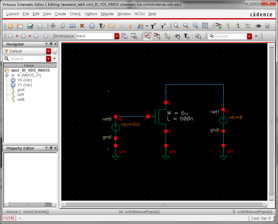
Here the 4th pin, the body connection, of the NMOS is not shown because it has been implicitly tied to gnd. The voltage source
on the far left shows vdc=VGS. VGS will be used as a variable for a parametric sweep in the lab simulations.
My second layout from Tutorial 2:

Again, please ignore the m2 and m3 traces for now.
Similar to the n-channel MOSFET, the p-channel MOSFET also requires 4 pins, gate (G), source (S), drain (D), and body connection (B).
In the case of the PMOS, the body connection must be tied to vdd! or the highest voltage in the circuit to operate properly.
Although
the voltage used in a digital circuit is typically 5V, vdd! can be any
value so long as it is the circuit's largest voltage.
Schematic of circuit that simulates PMOS operation:

In contrast to the NMOS circuit, the body connection of the PMOS in the circuit above is shown, and it is tied to vdd!.
The voltage source on the far left shows vdc=VSG. VSG will be used as a variable for a parametric sweep in the lab simulations.
Comparing
either the schematics or the layouts of the n and p-channel MOSFETs, it
can be seen that p-channel devices must be made
twice as wide as
their n-channel counterparts. This is due to the fact that a PMOS
resides in n-well which has a resistivity double that
of the p-substrate; thus the n-well section used for a PMOS must 2 times as wide to counteract this difference.
Lab:
The
first simulation is a dc analysis with a parametric sweep across VGS, the gate voltage,
and displays the current through the drain, ID,
of an NMOS vs. the voltage between the drain and the source, VDS. VDS varies between 0V and 5V in 1mV steps, and 6 graphs
are shown. Each represents a different value for VGS: 0V through 5V in 1V increments.
Simulation 1 - ID vs VDS for an NMOS device:

As is shown in the window, the purple trace represents VGS=5V, and the red trace represents VGS=0V.
The schematic used to generate this simulation is the NMOS circuit built and shown in the pre lab.
The second simulation is another dc analysis showing the current through the drain of an NMOS, ID, vs. the gate voltage, VGS.
For this simulation, VDS was held at a constant 100mV.
Simulation 2 - ID vs VGS for an NMOS device:

The schematic used to generate this simulation is the following NMOS circuit:

This is essentially the same circuit as the one used in Simulation 1. However, notice that the voltage source used
to represent VGS no longer uses a variable name because a parametric sweep was not needed for simulation 2.
Also notice that the VDS voltage source is now a constant value of 100mV.
The
third simulation is a dc analysis of the drain current, ID, vs. the
source-to-drain voltage, VSD, of a PMOS device. Note that in a PMOS
the
locations of the source and drain are reversed and also that the gate
voltage is measured between the source and the gate of the PMOS.
This
simulation also uses a parametric sweep and varies the gate voltage,
VSG, between 0V and 5V in 6 six steps (1V between each step).
VSD increases from 0V to 5V in 1mV steps.
Simulation 3 - ID vs VSD for a PMOS device:

The schematic used to generate this simulation is the PMOS circuit that was built and shown in the pre lab.
The fourth simulation is a dc analysis showing the current through the drain of a PMOS, ID, vs. its gate voltage, VSG.
For the simulation, VSD was held at a constant 100mV.
Simulation 4 - ID vs VSG for a PMOS device:

The schematic used to generate this simulation is the following PMOS circuit:

This is essentially the same circuit as the one used in Simulation 3. However, Simulation 4 did not utilize a parametric sweep,
and VSD in the circuit is now 100mV.
Now that the simulations have been completed, MOSFET and bondpad layout is discussed.
Layout of an NMOS with 4 bondpads and pins:
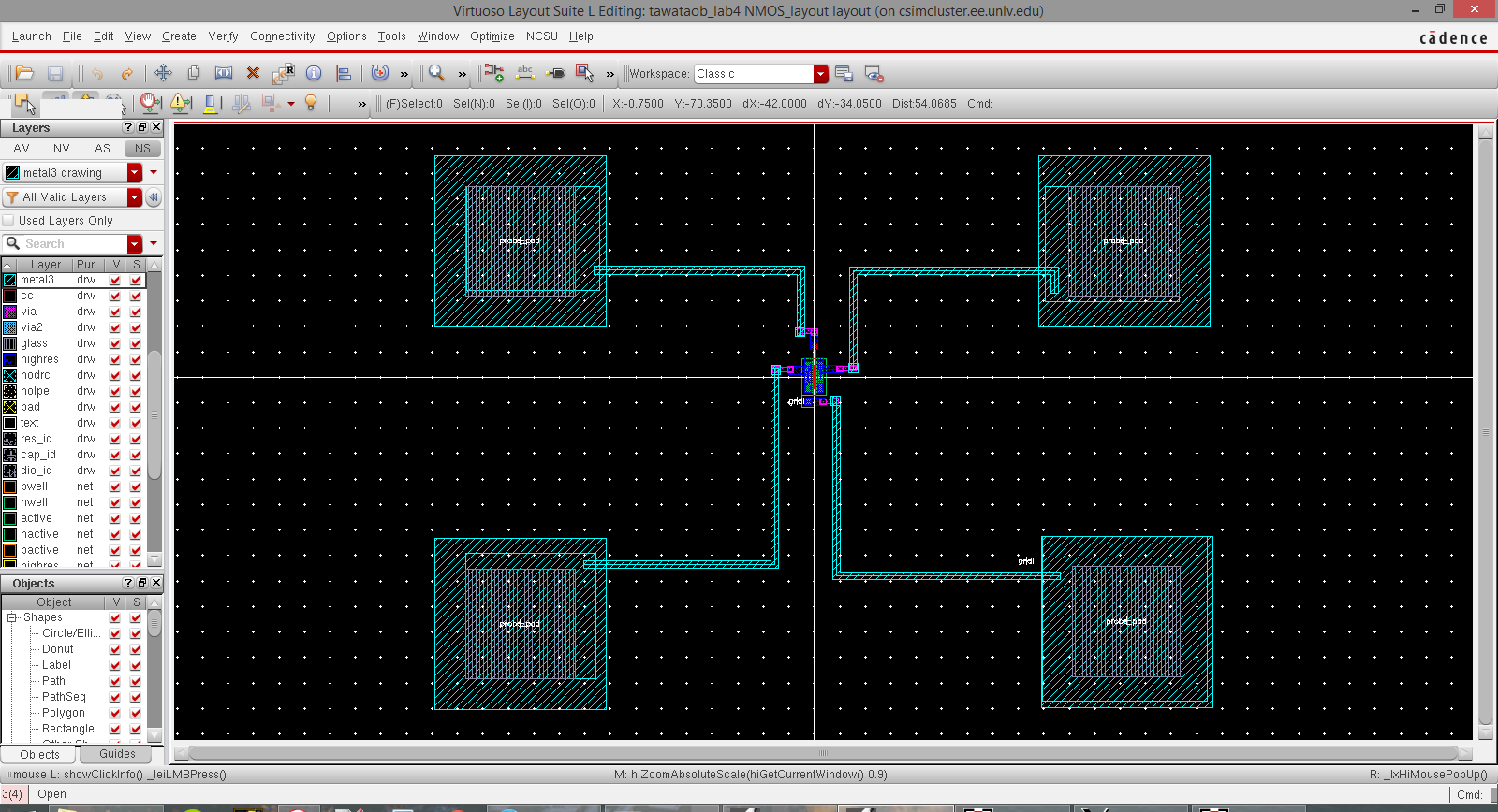
The
bondpads in this layout connect to metal3. However, all four of the
MOSFET terminals reside on metal1; thus via components were imported
from an NCSU library and used here.
Two vias were used for each
bondpad; metal1-metal2 and metal2-metal3 vias facilitated the
connection of each of the MOSFET pins to a bondpad.
In addition,
four new pins (G,D,S,gnd!) were created and placed on the bondpads;
these new pins correspond to those on the NMOS schematic, shown later.
Layout passes DRC:

Schematic corresponding to this layout:

NMOS LVS completes successfully:

PMOS layout with bondpads:
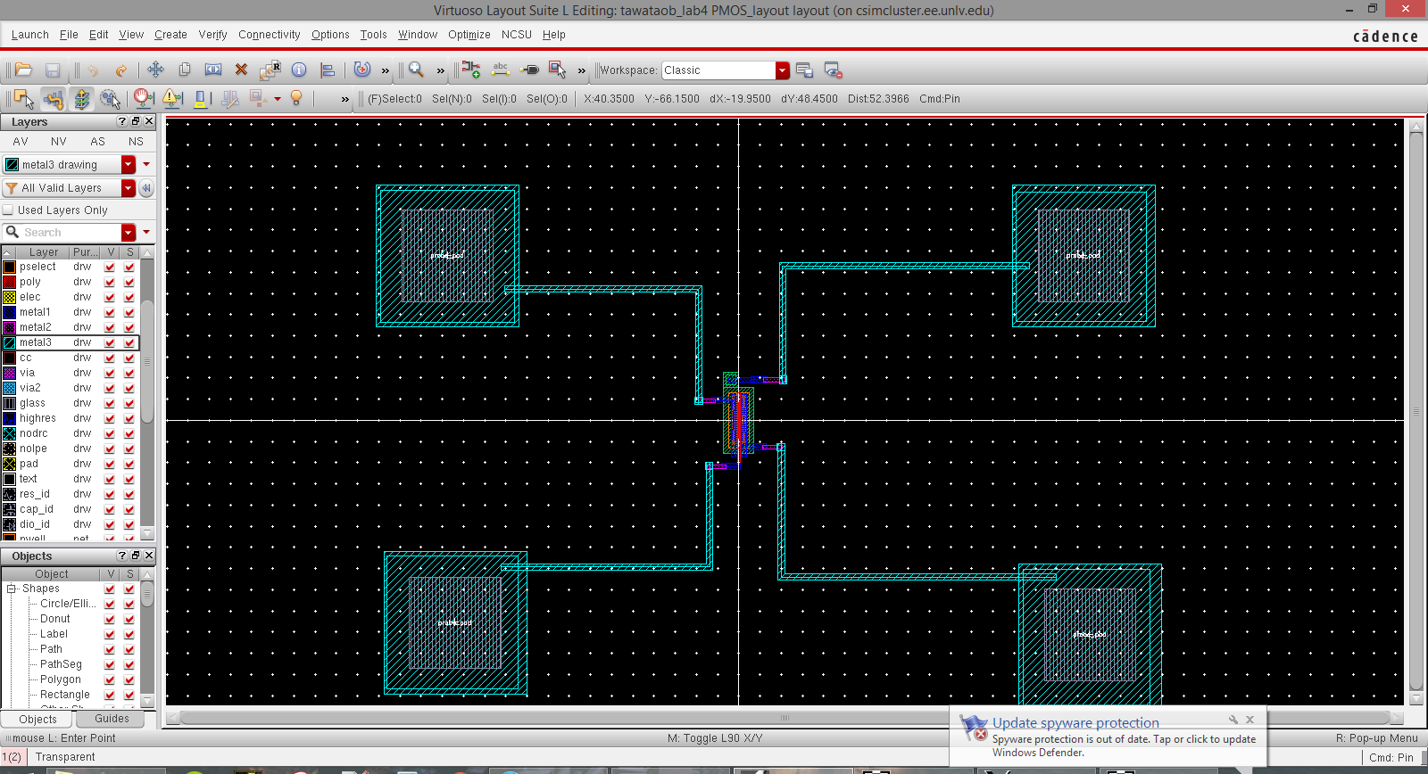
The
bondpads connect on metal3. Via components were again imported
from the NCSU library and used here.
Identical to the NMOS layout, two vias were used for each
bondpad; metal1-metal2 and metal2-metal3 vias facilitated the
connection of each of the MOSFET pins to a bondpad.
Four pins (G,S,D,B) were placed on the bondpads;
these new pins correspond to those on the PMOS schematic, shown below. The width of this PMOS device is 12 microns
which
is twice as large as that of the NMOS device whose width is 6 microns
and whose layout was shown earlier. The length of both MOSFETs,
however, is 0.6 microns or 2 lambda.
Layout passes DRC:

Corresponding 4-pin PMOS Schematic:

Successful PMOS LVS:

As always, this and all previous labs have backups in Dropbox:

The Lab 4 design directory can be found here.
Return to labs