Lab 2 - ECE 421L
Authored
by Silvestre Solano,
Email: solanos3@unlv.nevada.edu
9-22-2014
Lab
description
Prelab
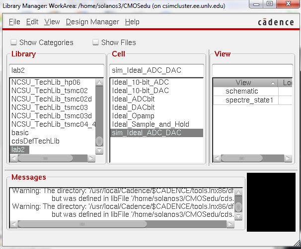
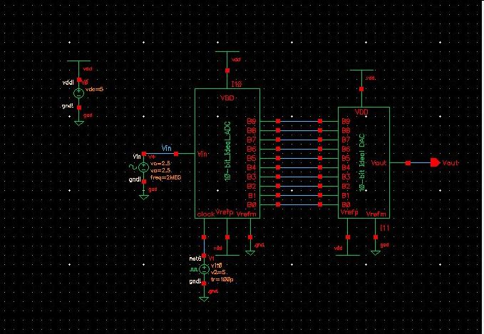
After login in and unziping the lab2.zip file, the schematic for the ADC/DAC will be selected as shown below.
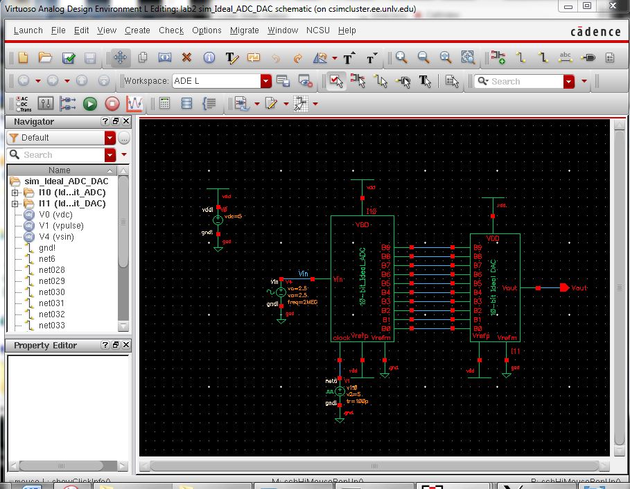
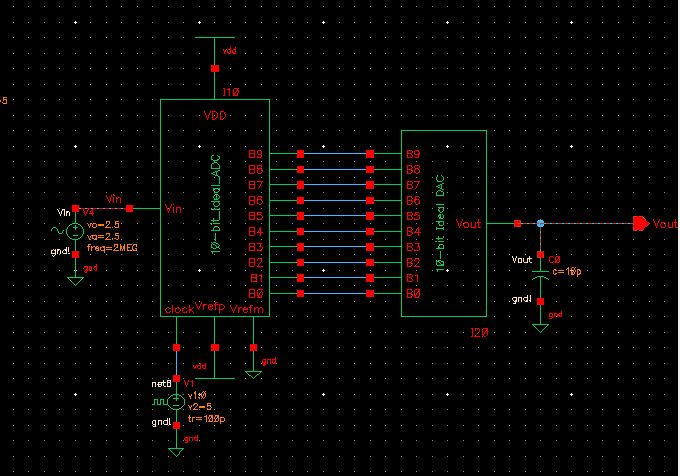
After clicking on "schematic", the schematic shown below should appear.
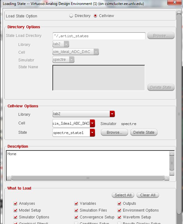
After launching the schematic, the ADE L will be loaded with the save state in cellview as shown below.
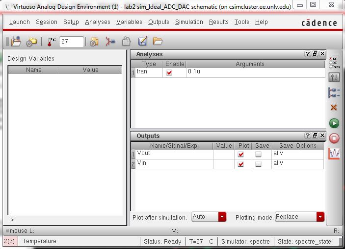
Then
the simulation parameters will appear and the green button will be
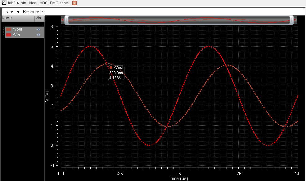
pressed as shown below. The simulation results are shown following the
picture below.
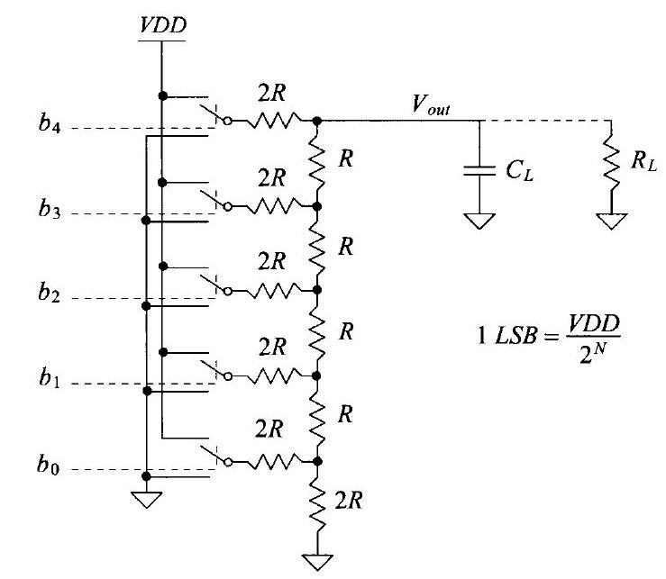
The LSB is found by the equation 1LSB=VDD/(2^n) were n is the number of bits of the DAC.
Postlab
The design of a 10-bit DAC using an
n-well R of 10k
In
this lab, we had to implement our own design for a 10-bit digital to
analog converter (DAC). This design is shown in the picture below.
The
first step in acomplishing this task is to first continue were the
prelab left off and copy "sim_ideal_ADC_DAC" into a new file called
"1_sim_ideal_ADC_DAC." After the copy is complete, the schematic shown
below will be used.
Using
the "Descend Edit" option on the DAC part of the above schematic
reveals the inside structure (shown below) that will be edited in order
to create the resistor based DAC.
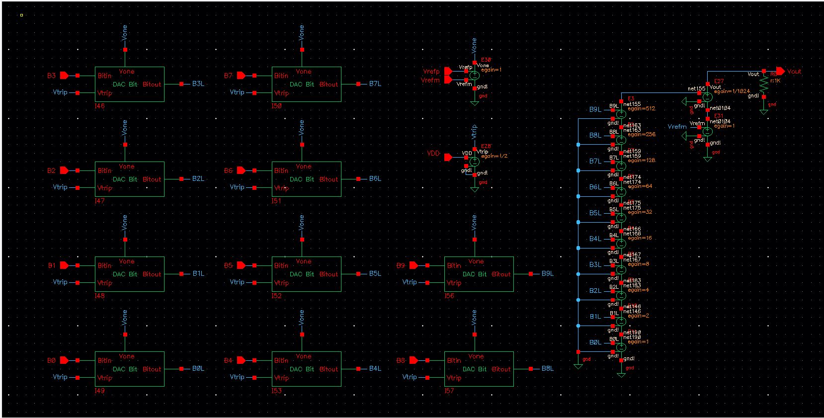
Everything
shown above will be completely erased with the exception of the B0-B9
input pins in order to make room for the resistor based DAC.
Unfortunately, this is the part were I screwed up the first time I did
the lab and I had to start all over with a new file called
"2_sim_Ideal_ADC_DAC."
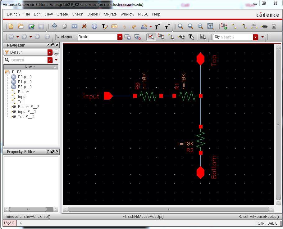
In a seperate file called "R_R2", I
created the simple resistor network as shown below. For some strange
reason, the 2R resistor had to implemented as two seperate resistors in
series. Pins are added in order to be used with the symbol view.
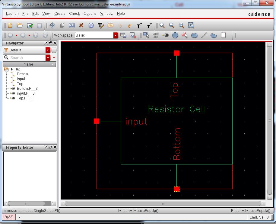
After
creating the resistor network, a new symbol view will be created for
it. The new symbol view that results from this is shown below.
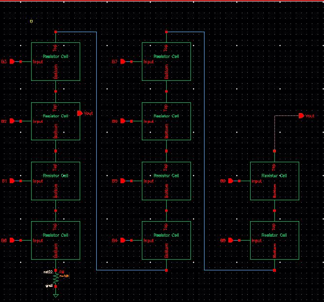
In
order to implement the 10-bit DAC, 10 of these resistor cells will have
to be strung up together in series within the original 10-bit DAC. The
completed interconnected resistor cell network is shown below. This is how you create a symbol view for the design that has the exact same footprint
as the Ideal_10-bit_DAC symbol view.
Simulations to verify your design
functions correctly.
In
order to illustrate that the resistor based DAC works correctly, I will
run a simulation of its output and display it below this sentance.
Originally,
I could not get my simulaion to work. I spent the first week of this
lab stuck in the same spot because my simulation would not run. On the
second week, I was still working on this problem until I decided to ask
professor Baker for help. He spent a good 5 minutes trying to
understand what was wrong with my schematic. In the end, he somehow
fixed it, but I doubt he even knew what exactly was wrong with my
schematic.
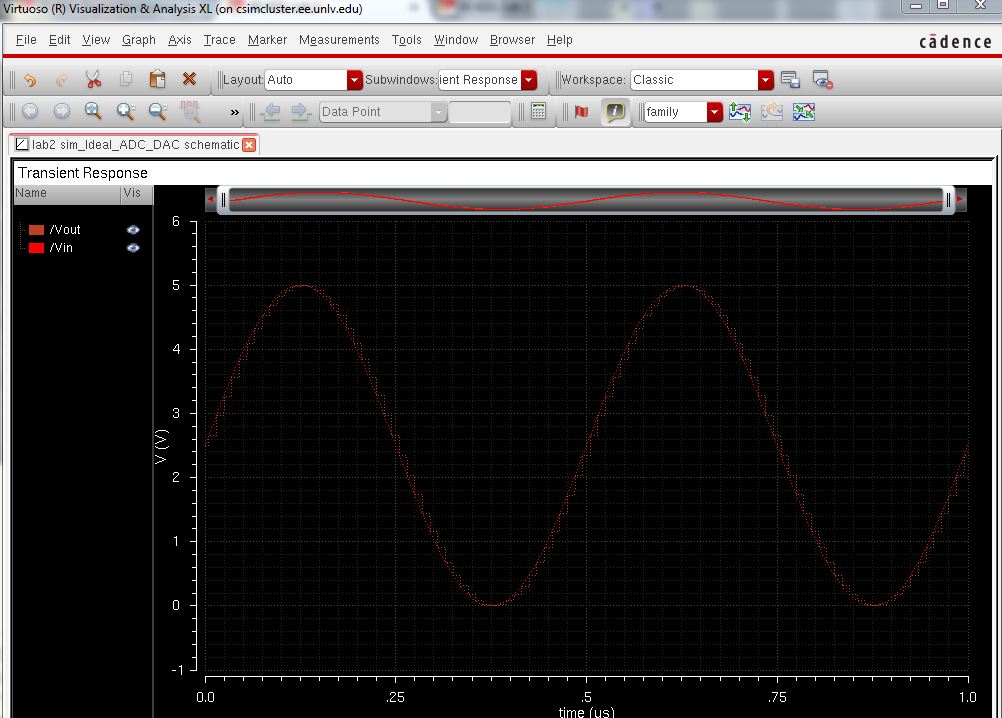
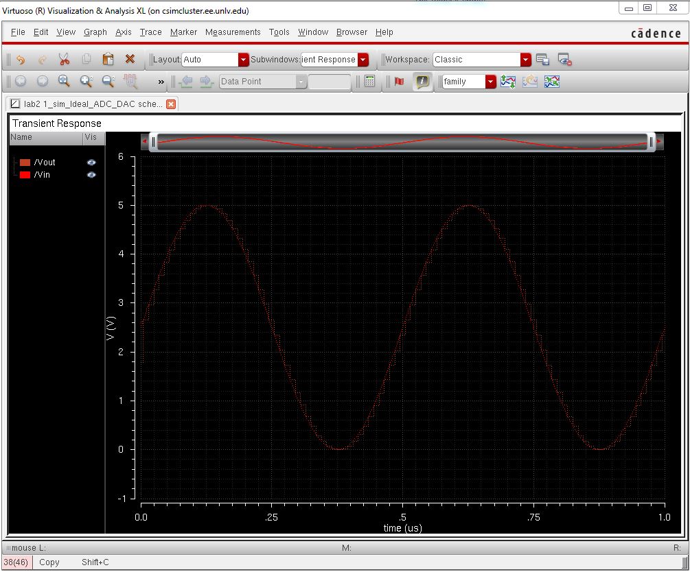
When
the circuit drives a 10pF load (shown below), the following output
voltage is shown on the graph that follows the schematic.
When
the circuit drives a 10pF load and a 10K resistor (shown below), the following output
voltage is shown on the graph that follows the schematic.
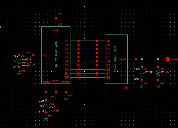
When
the circuit drives a 10K resistor (shown below), the following output
voltage is shown on the graph that follows the schematic.
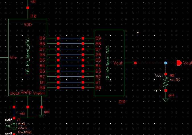
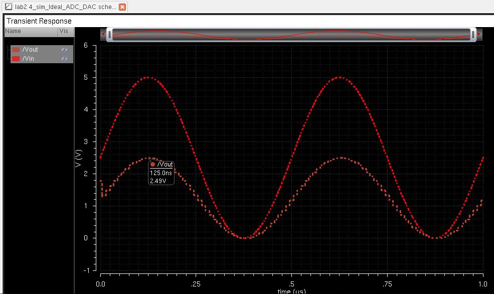
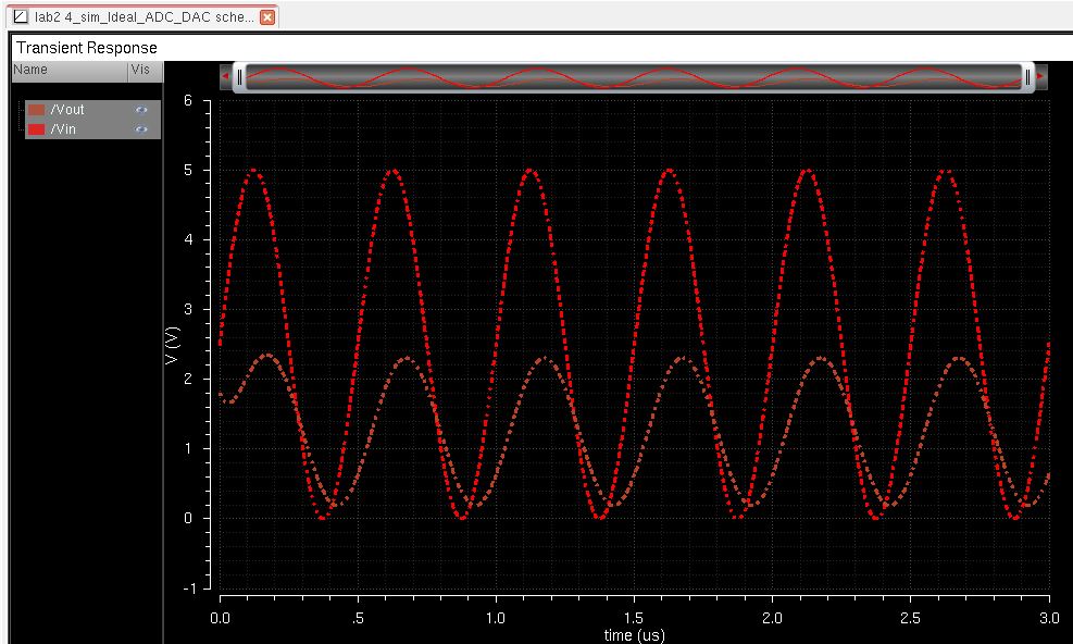
When
the DAC drives a 10k load, the output voltage is cut in half. This is
because the output resistance of 10K works with the load to form a
voltage divider that essentially cuts the outgoing voltage in half. In
the above grapy, the input voltage is 5 while Vout is 2.49 volts..
Delay, driving a load.
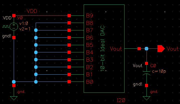
Ib
order to simulate the delay of a 10pF capacitor, the B0-B8 inputs of
the DAC will be grounded and a 1V pulse source will be added to the B9
input, as shown below.
The simulation results are shown below for the above circuit.
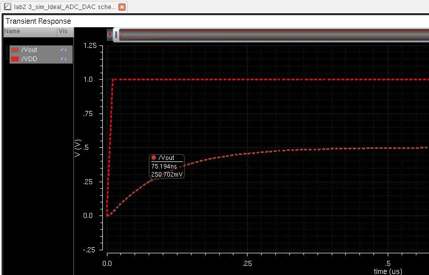
Because
the output voltage follwows the equation 1LSB=(VDD/(2^n)), which in
this case n=1, the output voltage will only be half of VDD. The
capacitor will only have a maximum charge o 0.5V, and the above
simulation result shows that the capacitor will reach half of its
maximum voltage (250mv) in about 75.194ns. Using the equation td =
0.7RC, where R is the total output resistance of 10k, the calculated
delay is 70ns. The simulated time delay and the calculated time delay
are very, very close.
How to determine the output resistance
of the DAC (answer: R) by combining resistors in parallel and
series
The
output resistance is determined by simply starting at the bottom of the
resistor network and combining the parallel resistors of 2R. This lead
to a simplified result of a resistance R, which adds with the other R
in series adding up to another 2R. This process continues until the B9
resistors. Eventually, it all simplifies to an output resistance of R.
Discuss what
happens if the resistance of the switches isn't small compared to R
If
the resistances of the switches isn't low, then the resistance of the
switches may or may not cause an undesired voltage drop across the
switches.
Return to the main lab directory.