Lab Project - ECE 421L
Design,
layout and simulate an 8-bit ALU that can perform A OR B, A ANDB, A+B and A-B
Prepared by:
For
this lab we will be using the logic gates designed in lab 7 to design an 8-bit
ALU. The ALU will have 3 inputs (A, B, F) and 1 output (Z). The ALU will
perform the desired operation based on the given F input.
|
F0 |
F1 |
Operation |
|
0 |
0 |
A + B |
|
0 |
1 |
A - B |
|
1 |
0 |
A OR B |
|
1 |
1 |
A AND B |
LAB WORK:
The first
operation needed to be performed is our OR function. For this we took our 2 bit
NOR gate, added an inverter onto the end and cascaded it into an 8 bit OR gate.
|
|
|
|
|
|
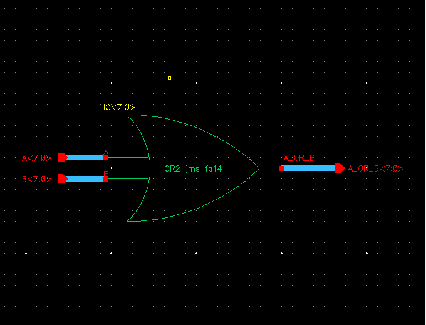 Fig 1
Fig 1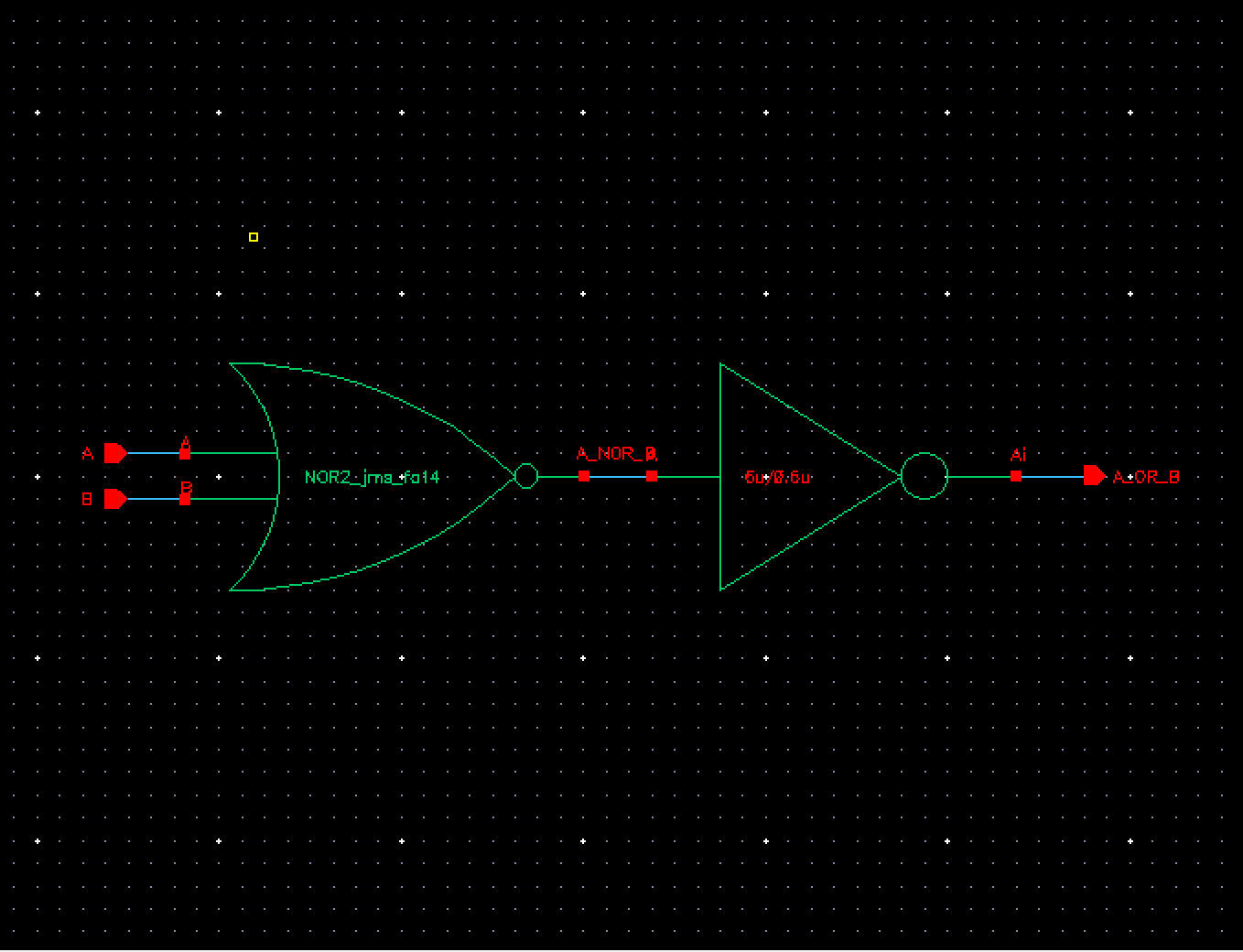 Fig 2
Fig 2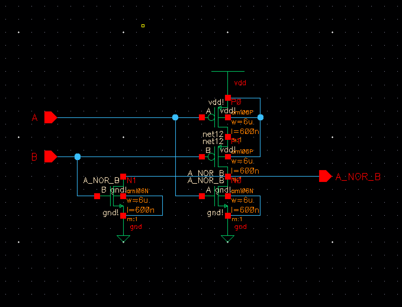 Fig 3
Fig 3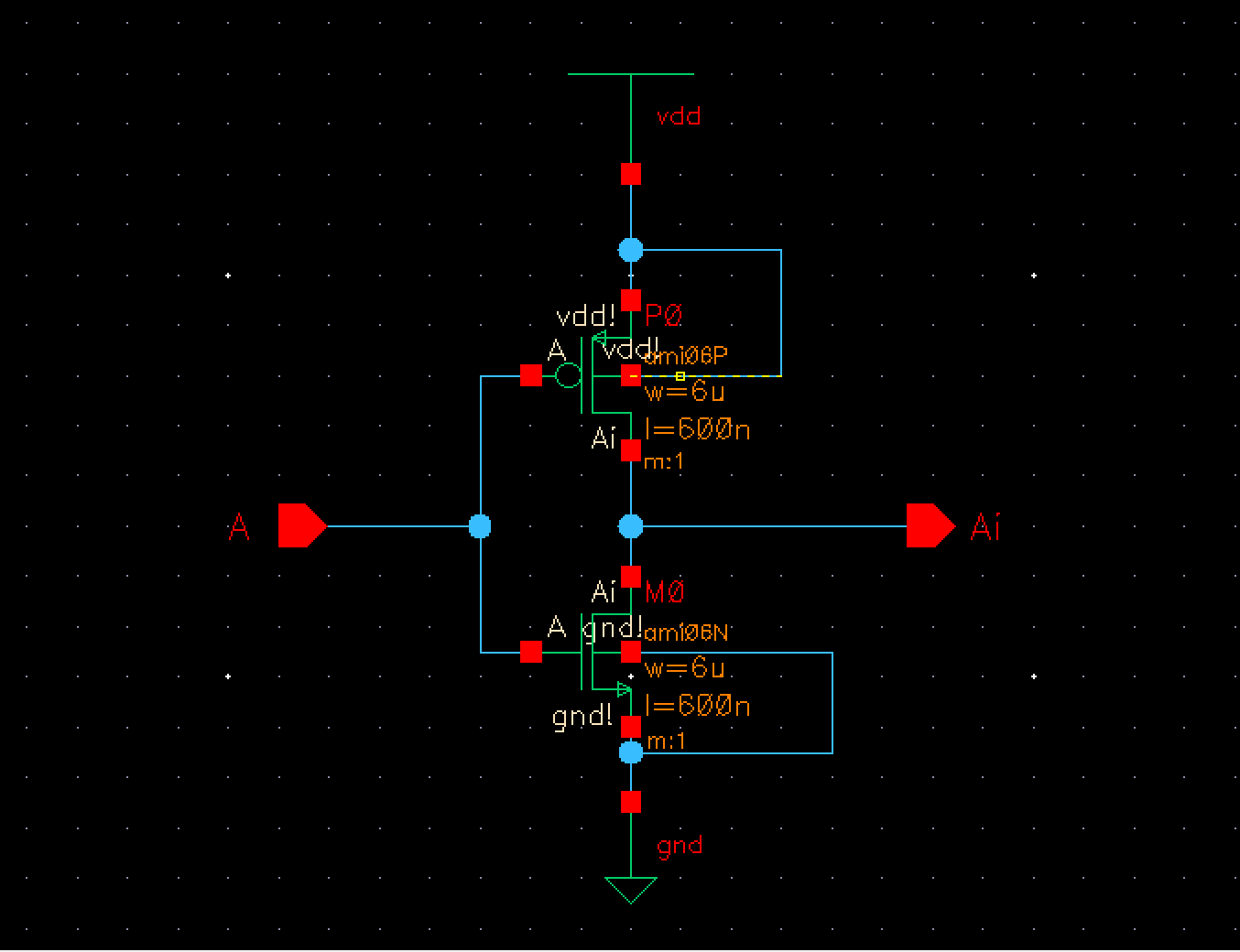 Fig 4
Fig 4The second
operation needed to be performed is our AND function. For this we took our 2
bit NAND gate, added an inverter just as we did in the previous step and then
cascaded it into an 8 bit AND gate.
|
|
|
|
|
|
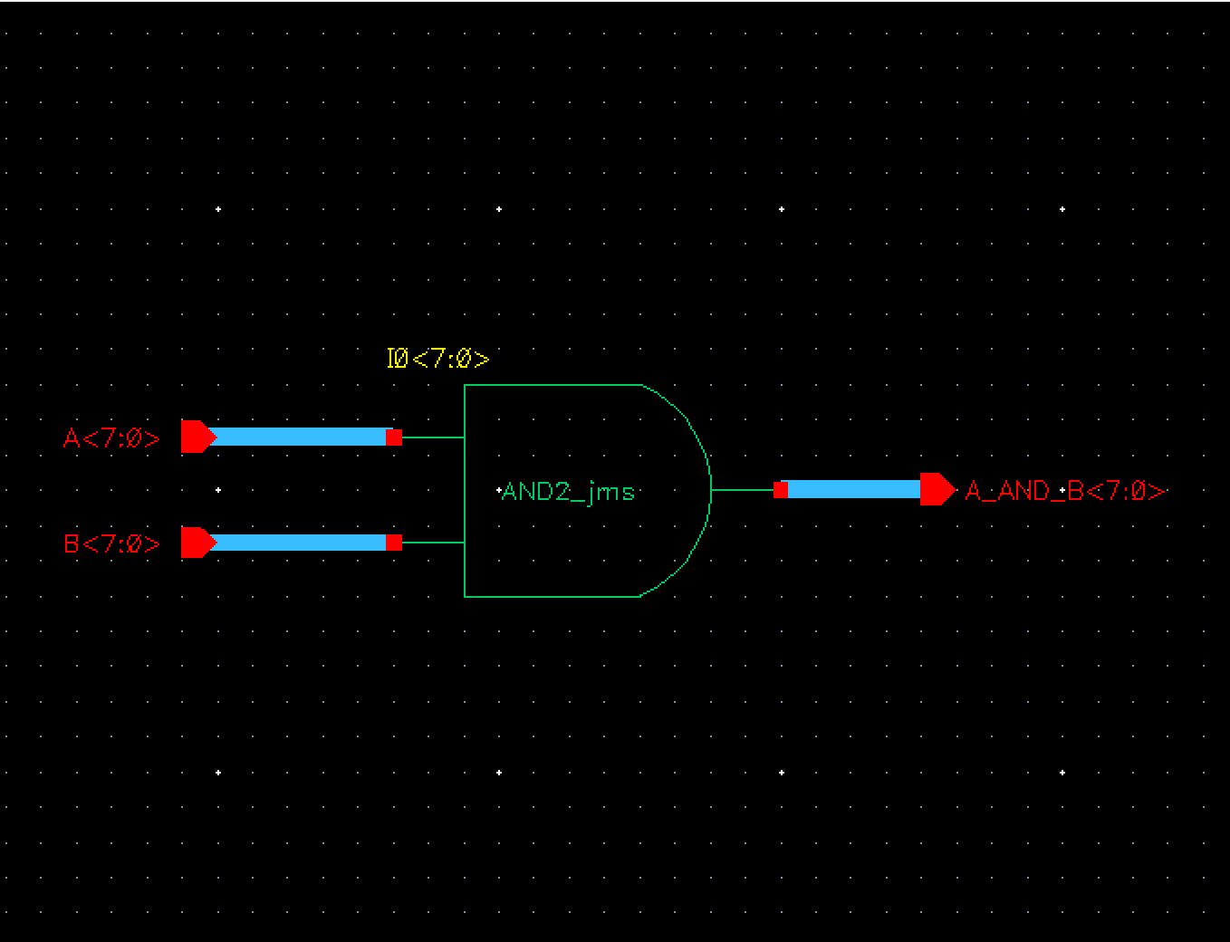 Fig 5
Fig 5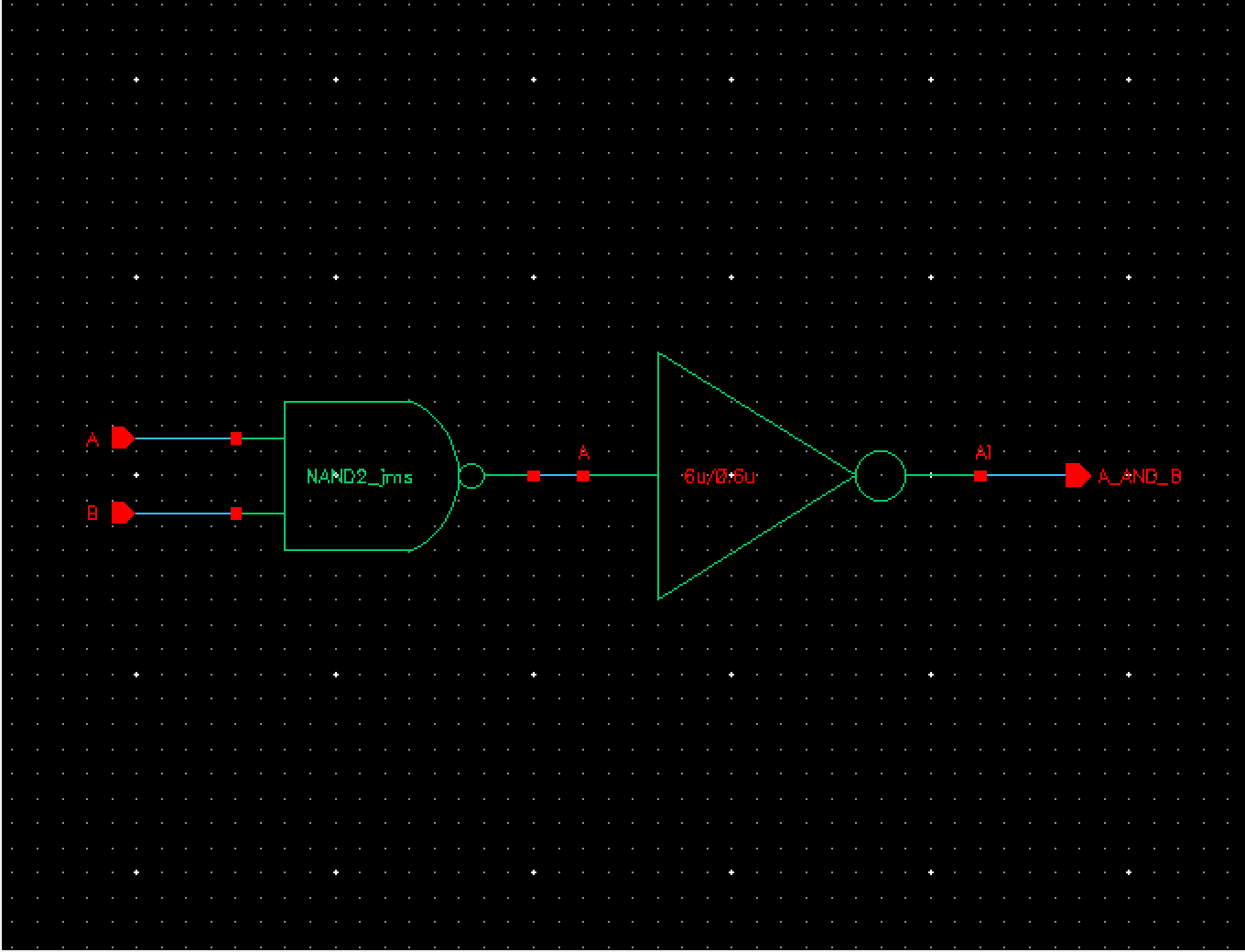 Fig 6
Fig 6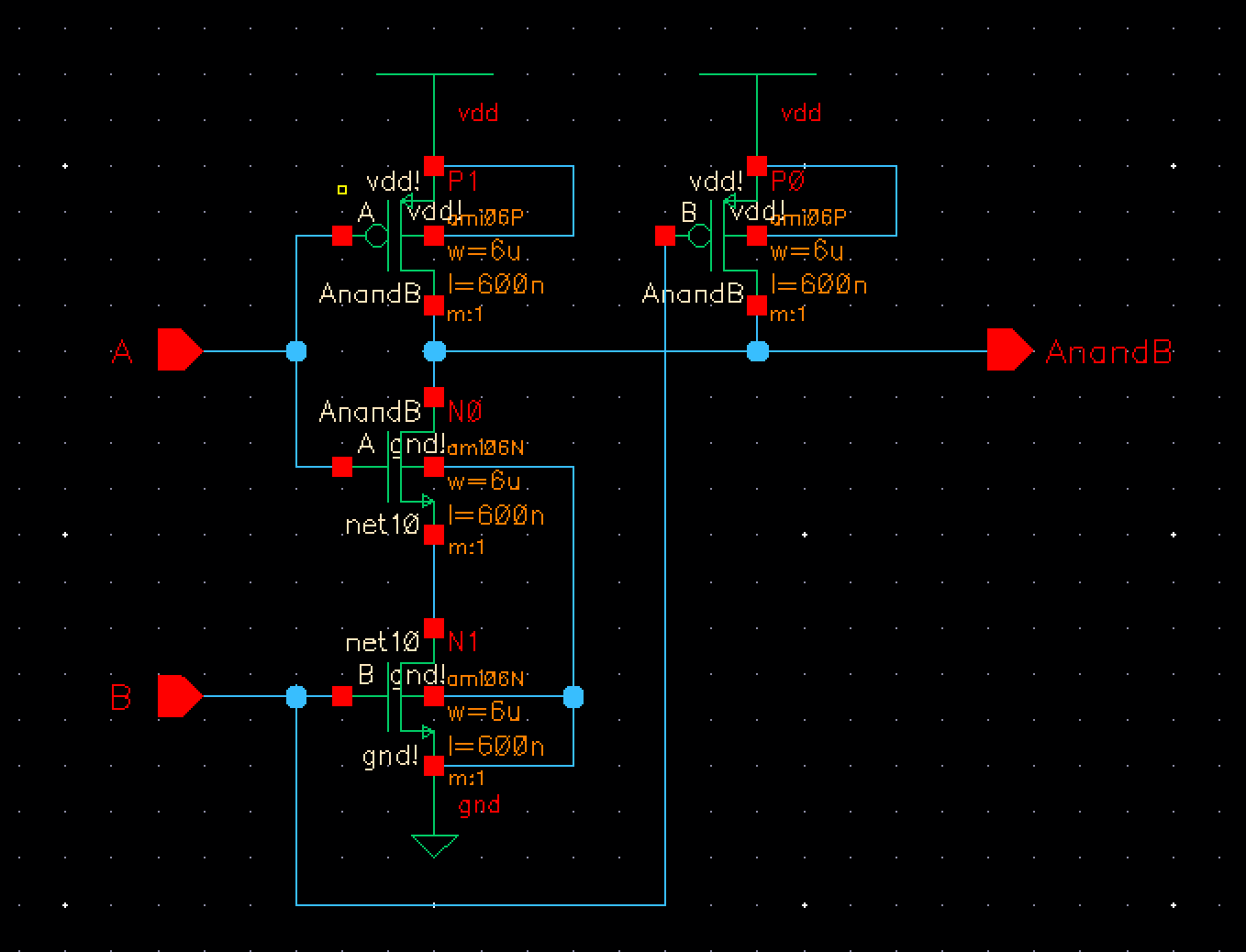 Fig 7
Fig 7The third
operation needed to be performed is our 8bit ADD function. To perform this we
used the 8 bit full adder we designed for lab 7.
|
|
|
|
|
|
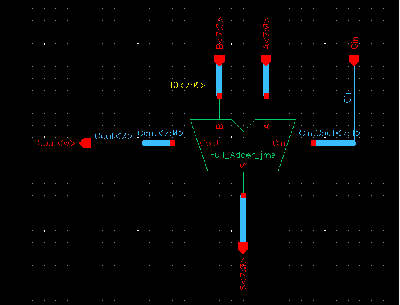 Fig 8
Fig 8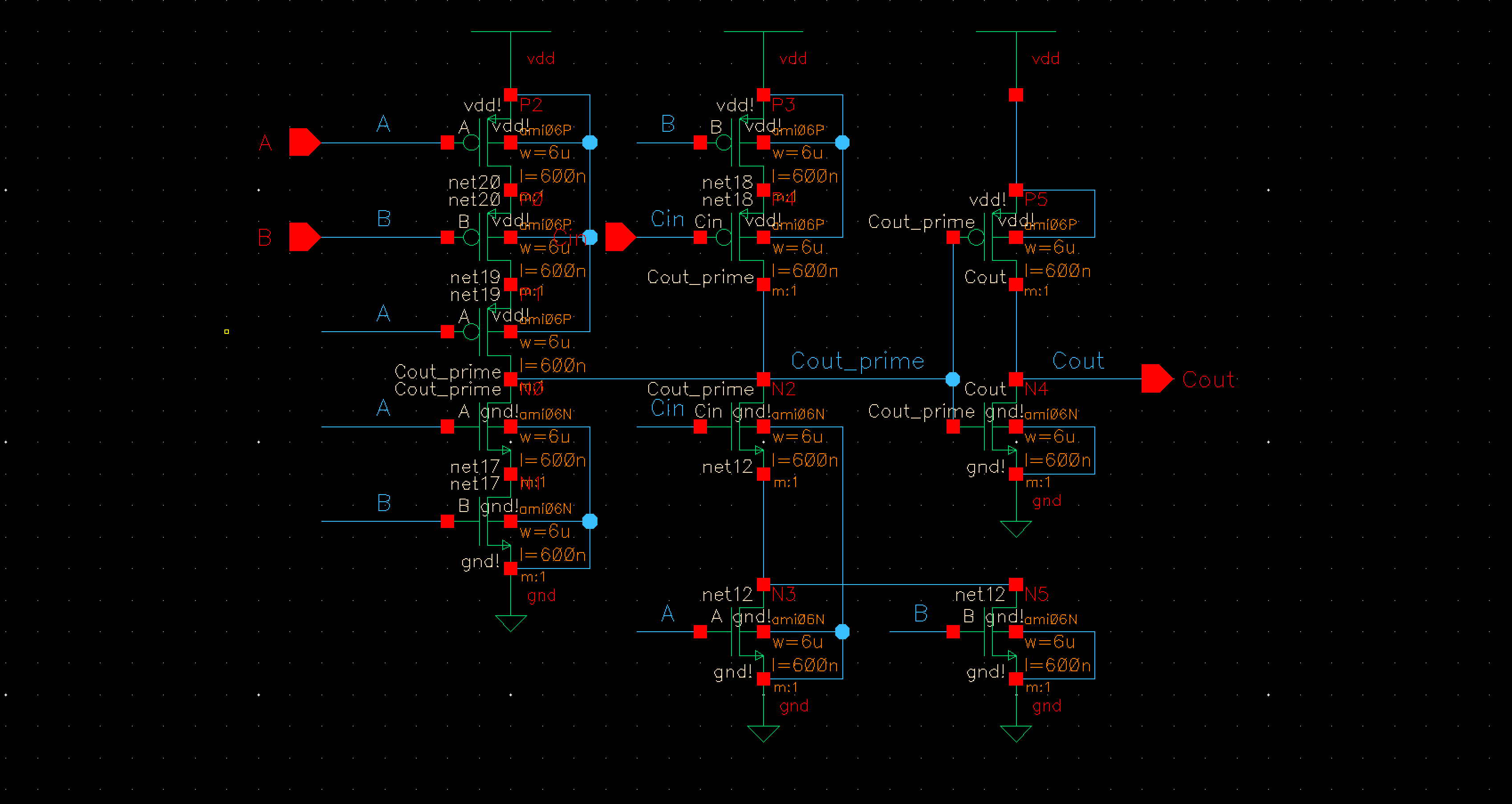 Fig 9
Fig 9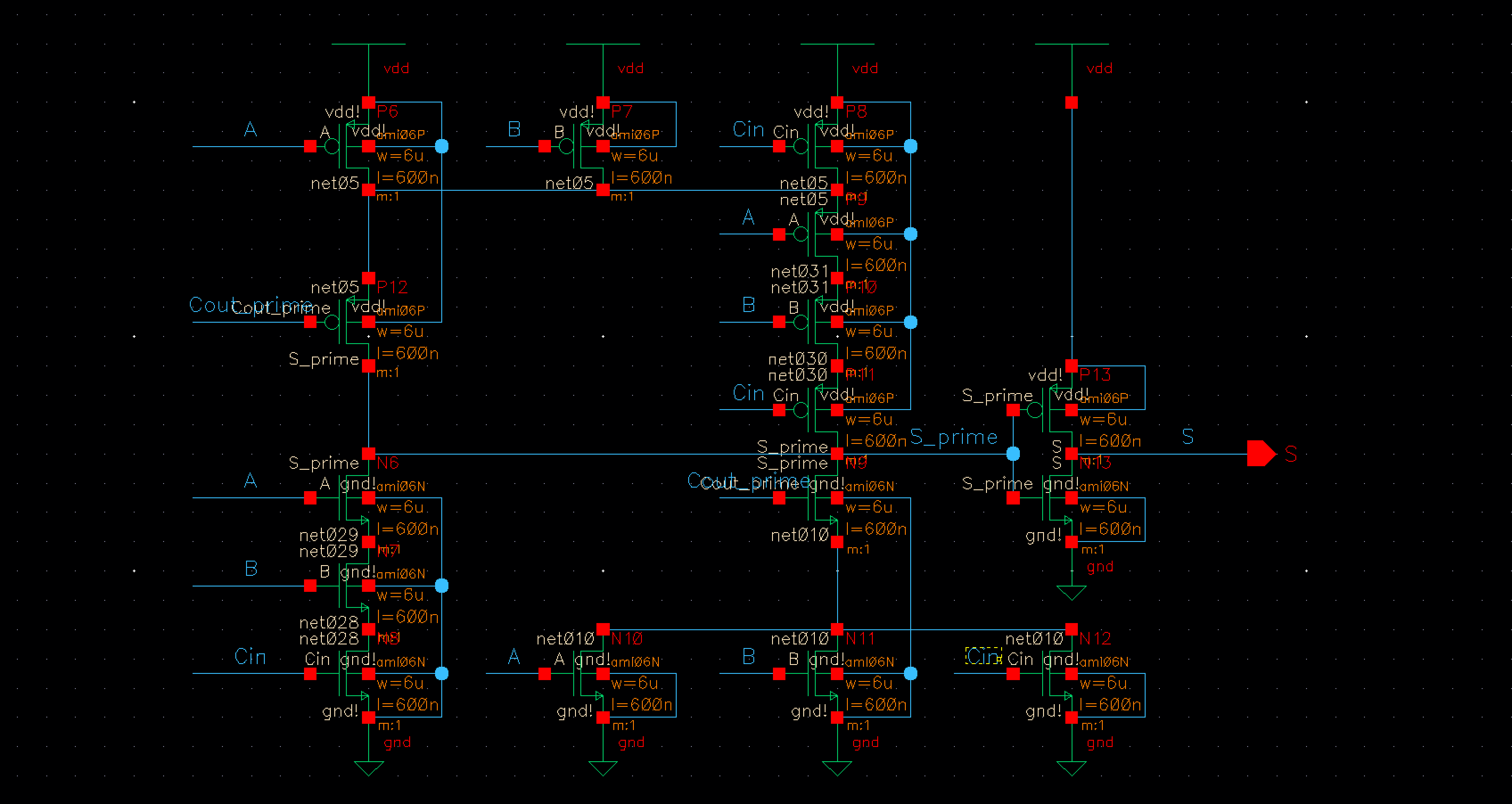 Fig 10
The final
operation needed to be performed is the 8bit SUBTRACTION function. To perform
this we used the same 8 bit full adder as the add function. To get the adder to
perform subtraction instead of addition, we used an 8 bit XOR gate to invert
our B input and our carry in signals. To perform the inversion we used our F1
input. When F1 is 0 there is no inversion and addition is performed. When F1 is
1 the inversion is performed and the adder adds the 2's compliment of the B
input, thus giving the subtraction solution. For this the following XOR gate
was used
|
|
|
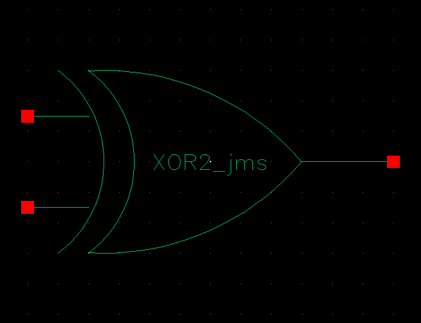 Fig 11
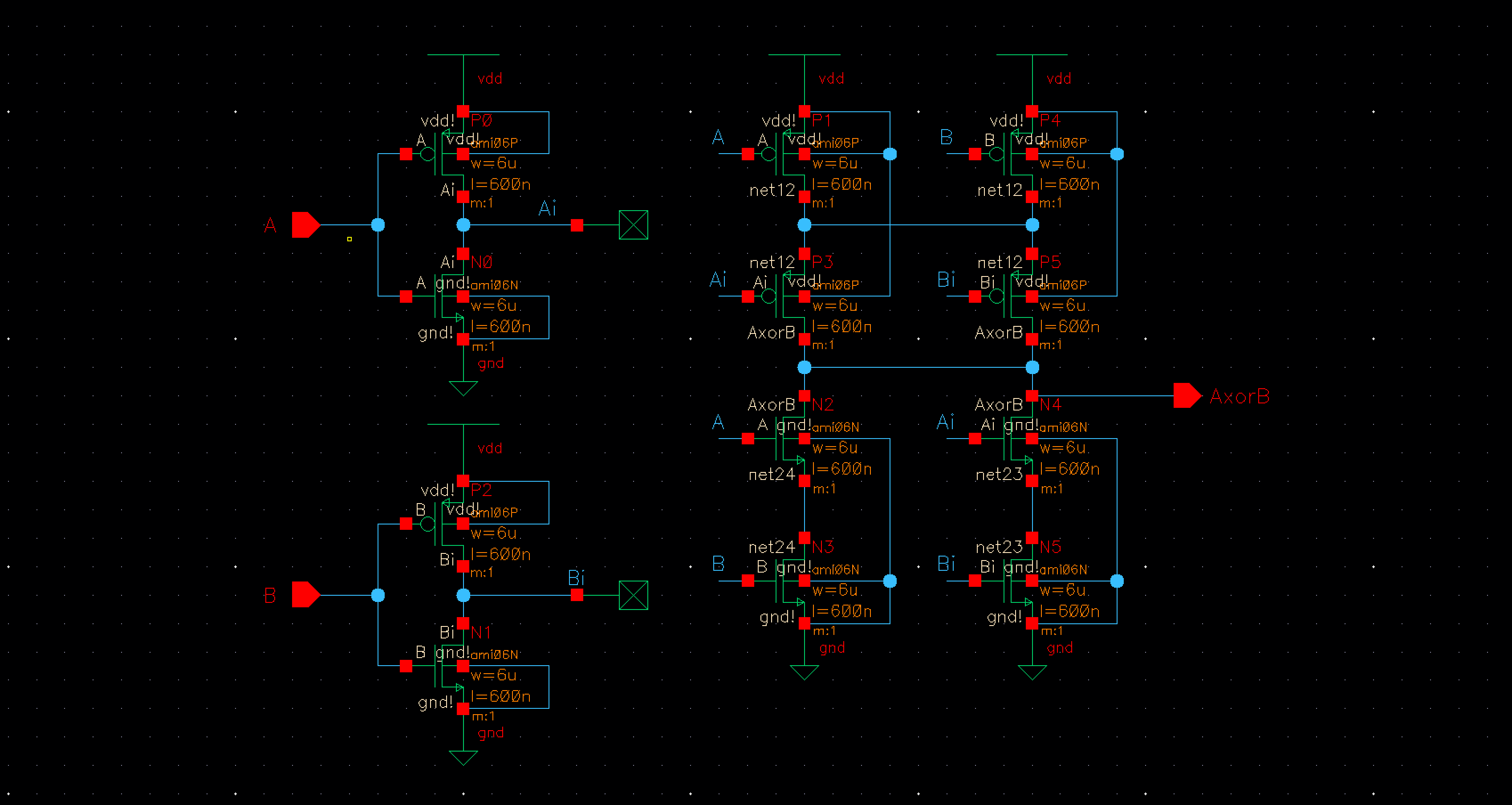 Fig 12
In order to
get the desired output from our selection we used an 8 bit Multiplexer. The
multiplexer could not be cascaded in the way the logic gates were due to the
single S input.
|
|
|
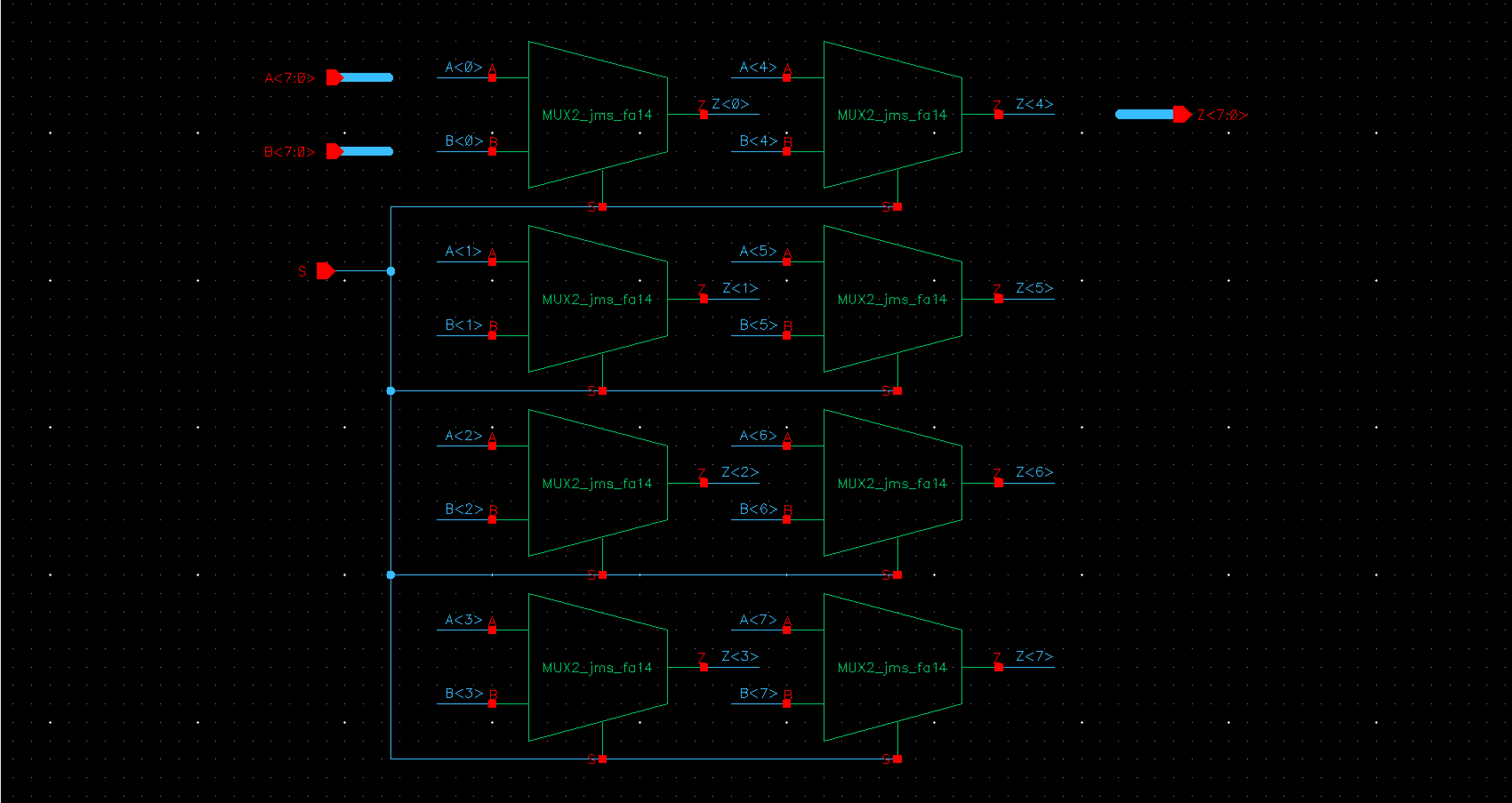 Fig 13
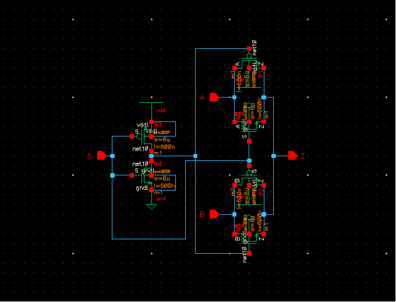 Fig 14
This led to
the following overall design schematic and symbol of the ALU:
|
|
|
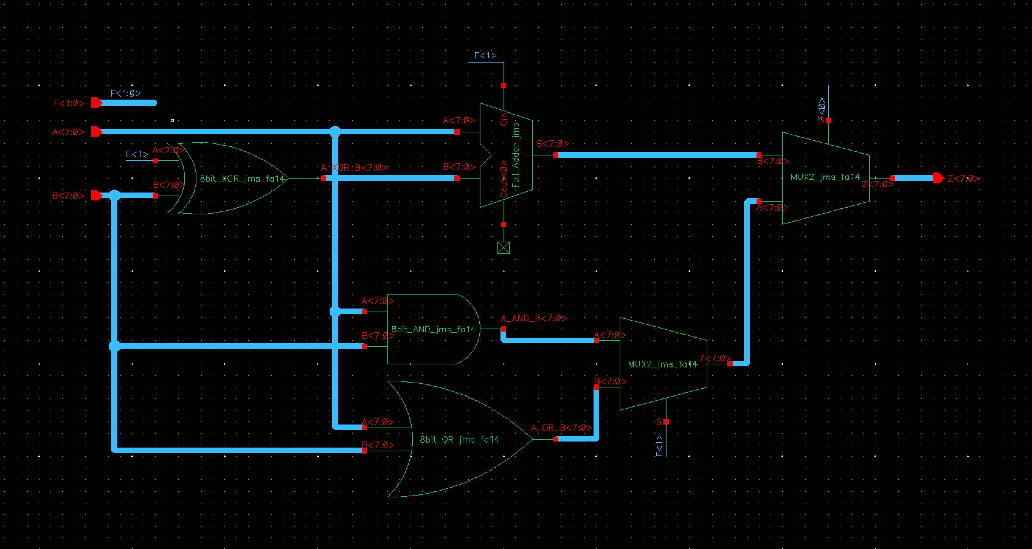 Fig 15
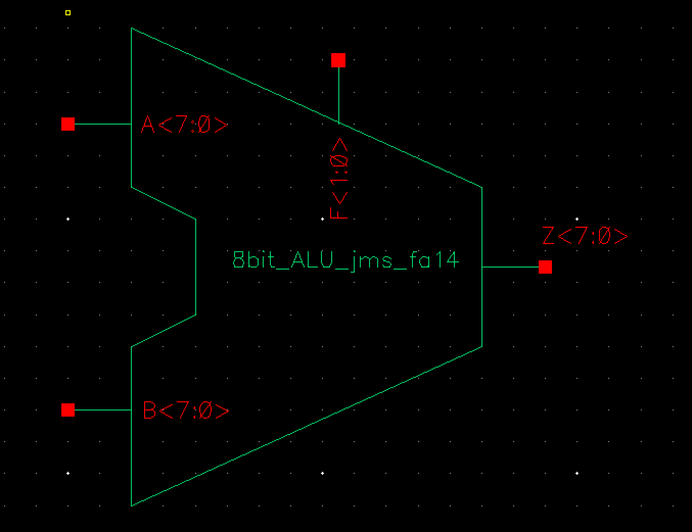 Fig 16
To ensure
the ALU performed as intended 2 different inputs were simulated, for the first
the following values were used:
|
A |
B |
ADD |
SUB |
OR |
AND |
|
00001100 (12) |
00000101 (5) |
00010001 (17) |
00000111 (7) |
00001101 |
00000100 |
|
|
|
|
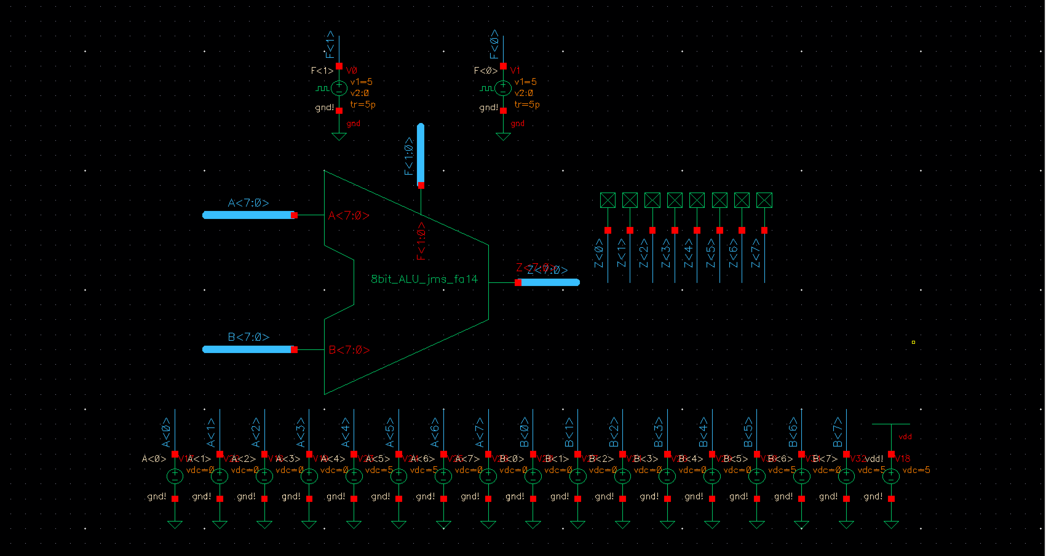 Fig 17
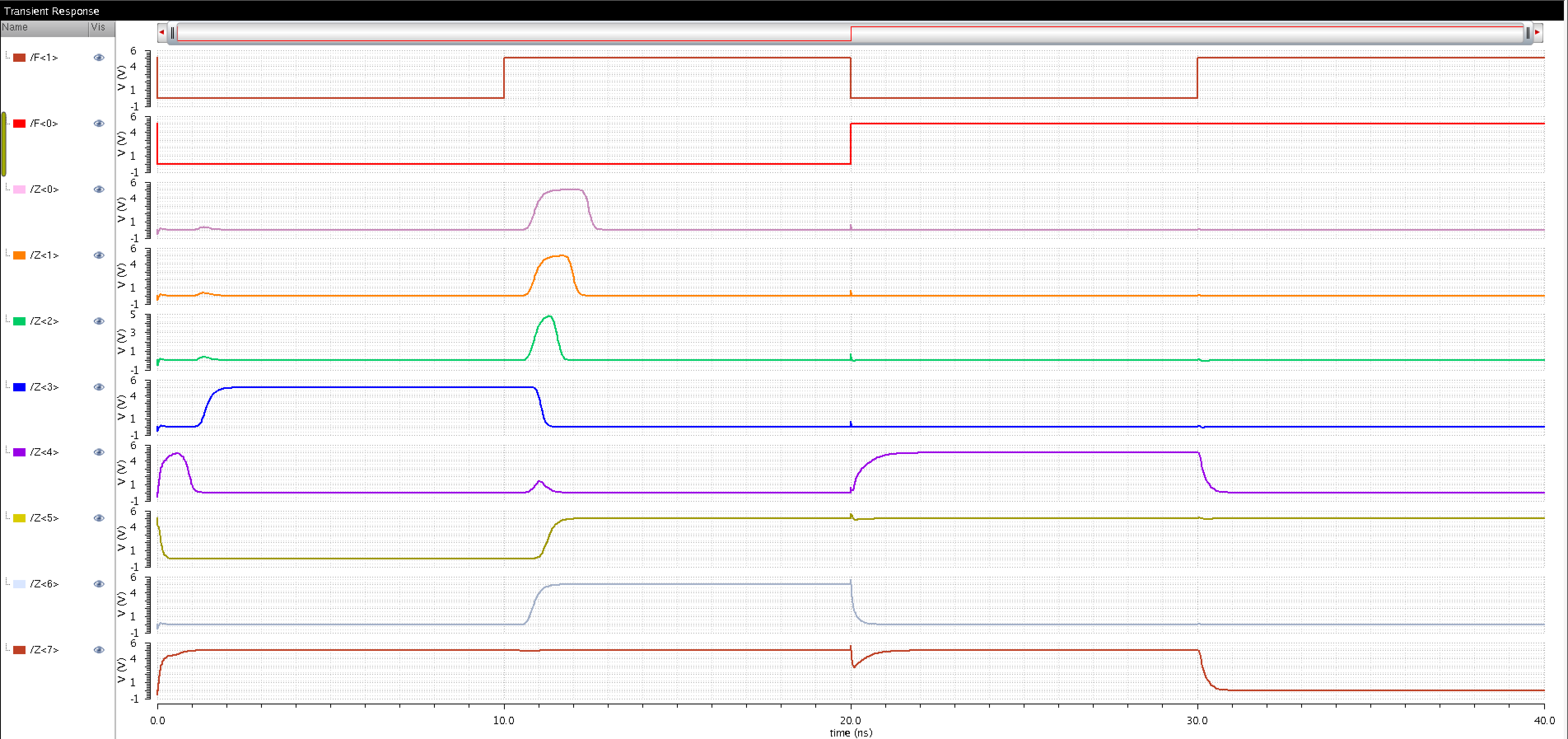 Fig 18
For the
second simulation the following values were used:
|
A |
B |
ADD |
SUB |
OR |
AND |
|
00011100 (28) |
00010100 (20) |
00110000 (48) |
00001000 (8) |
00011100 |
00010100 |
|
|
|
|
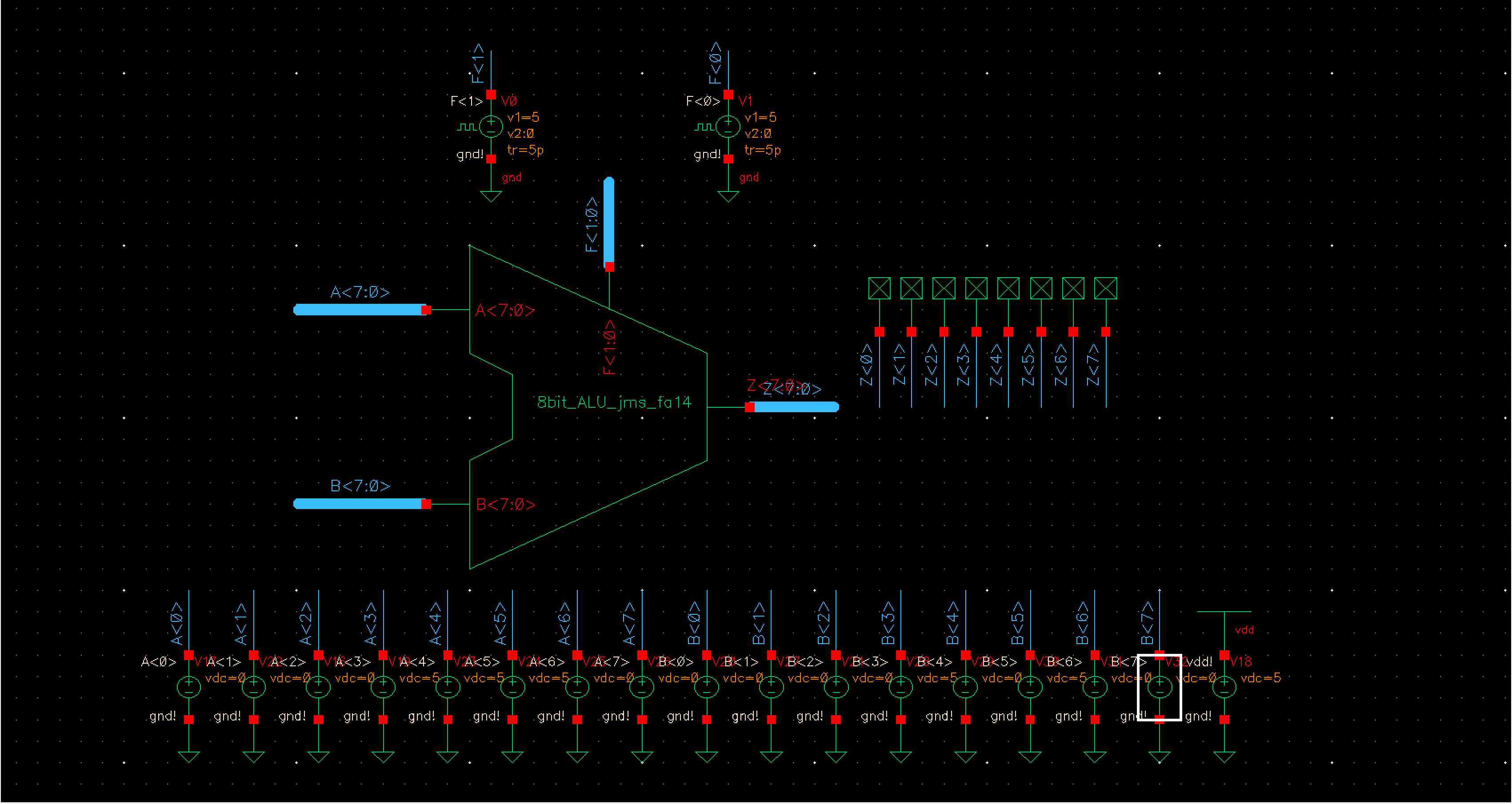 Fig 19
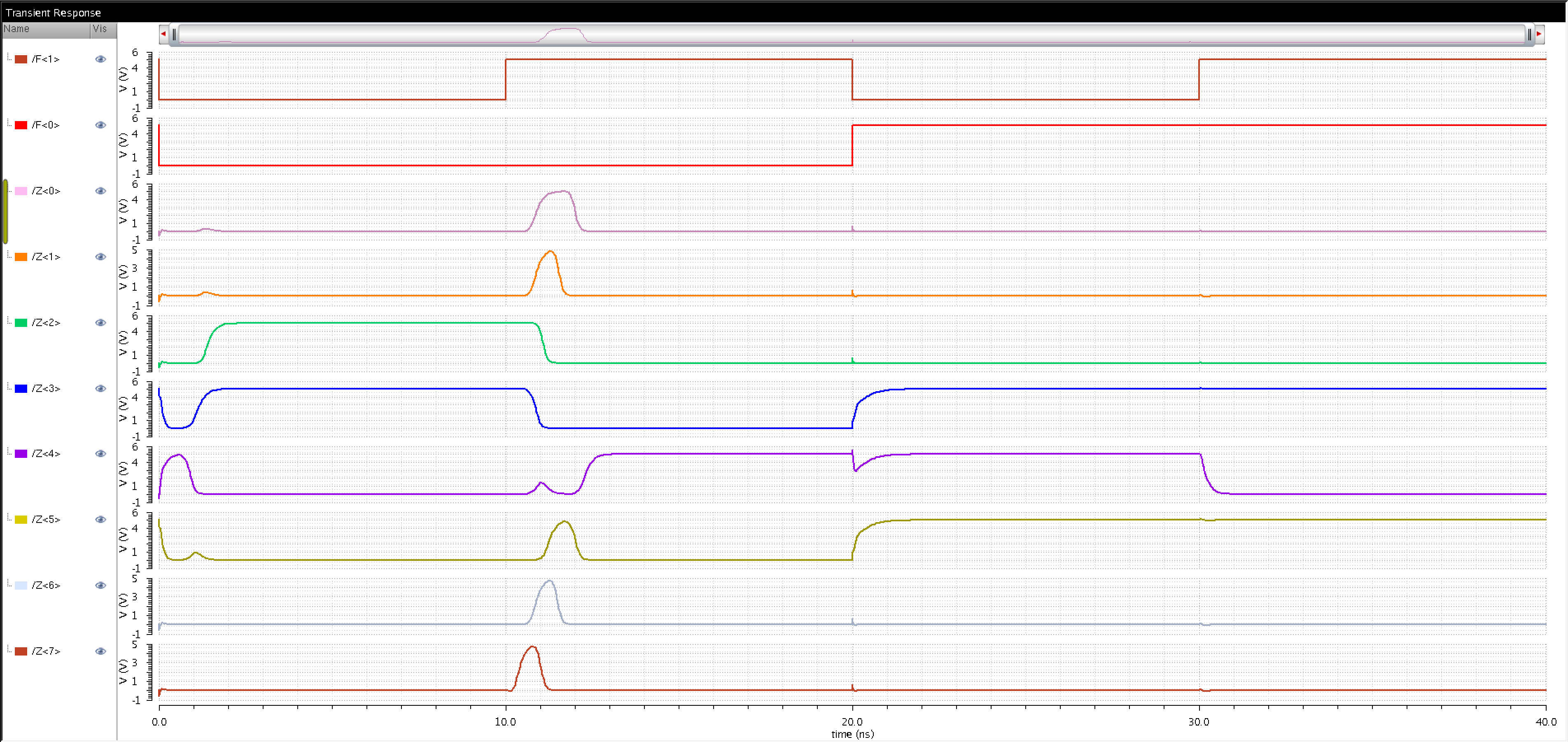 Fig 20
Part 2: Layout, DRC & LVS
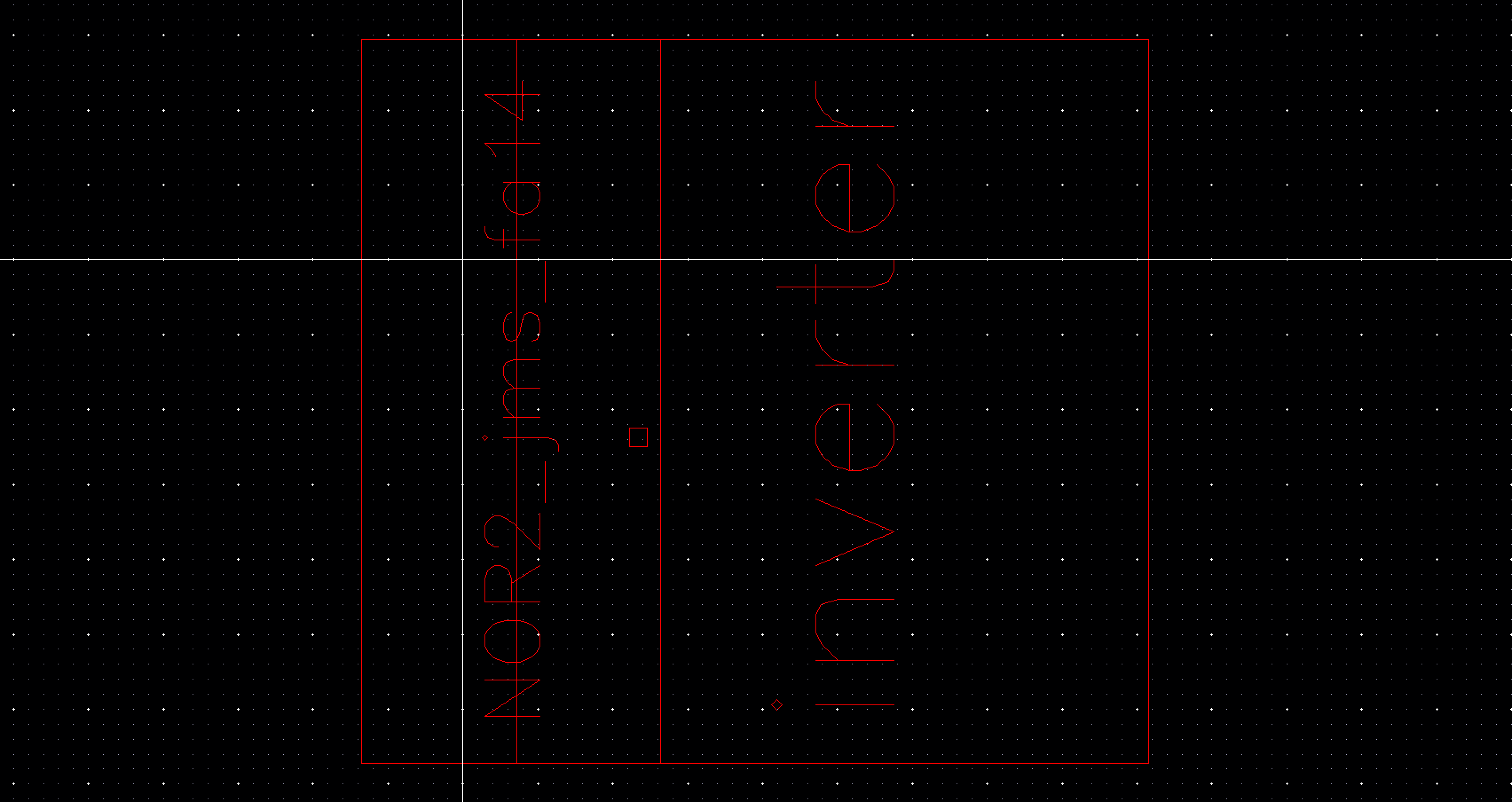
Fig 21
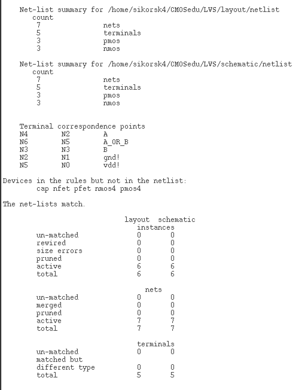
Fig 22
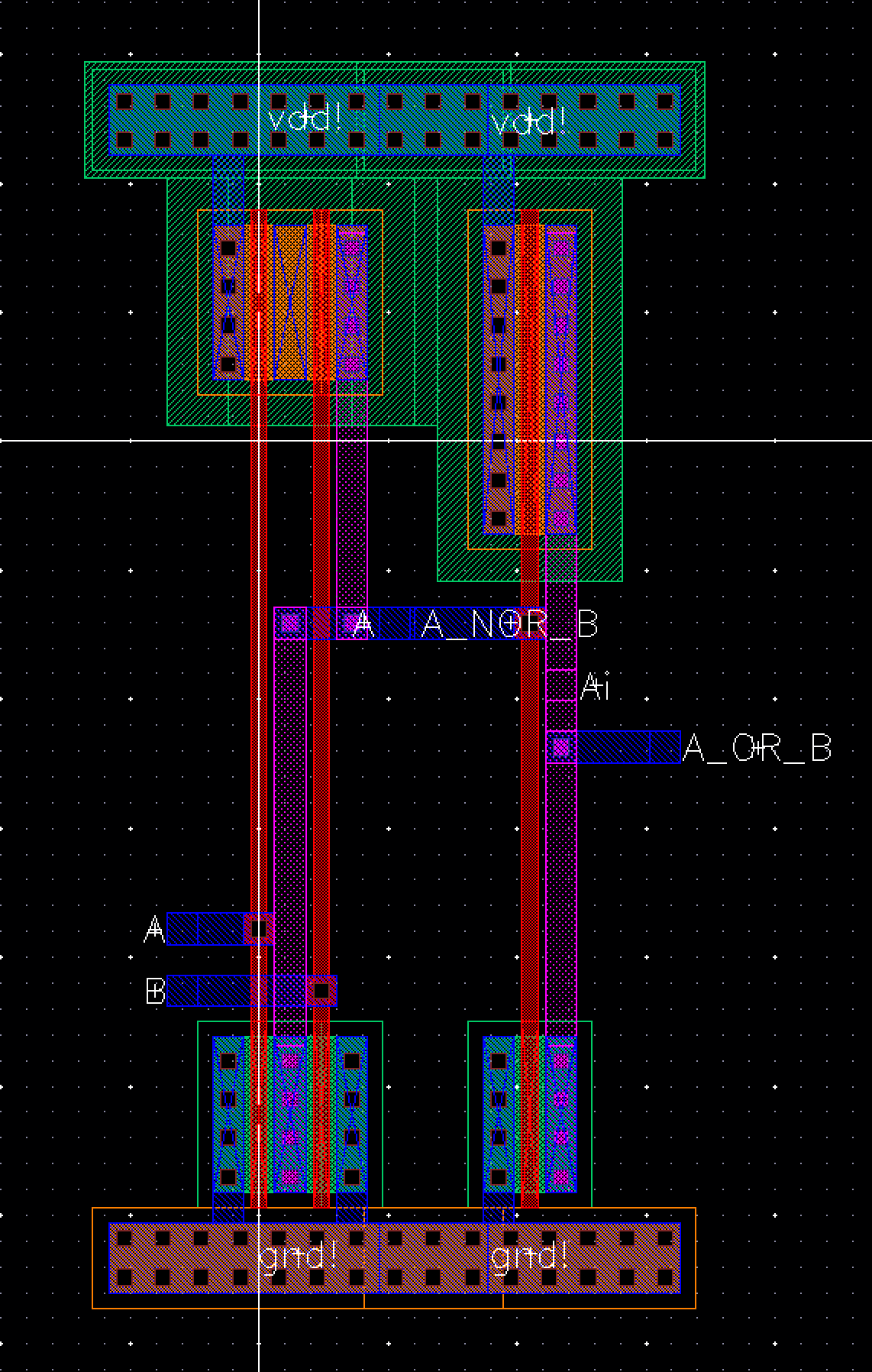
Fig 23
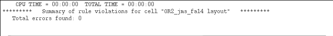
Fig 24
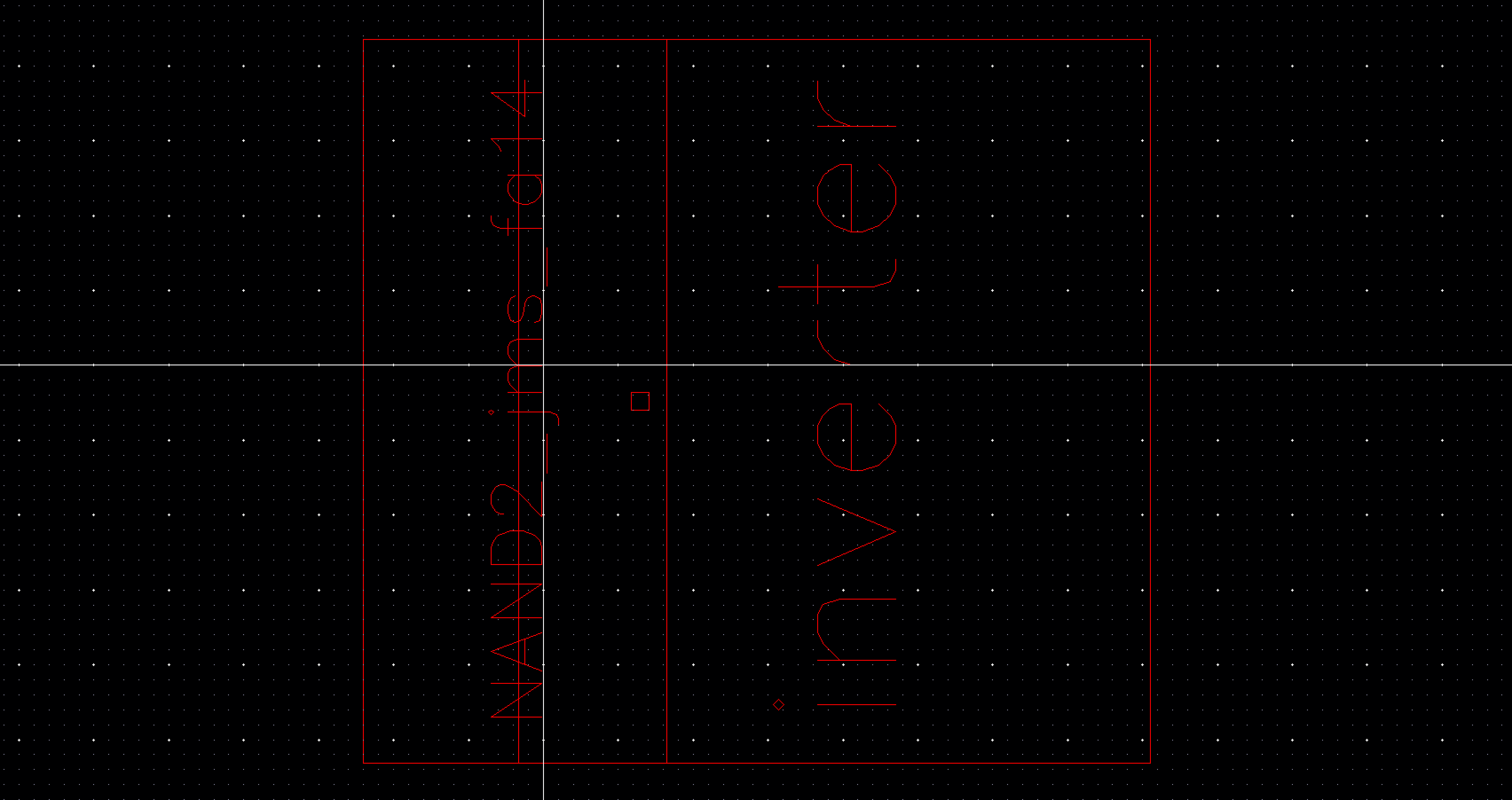
Fig 25
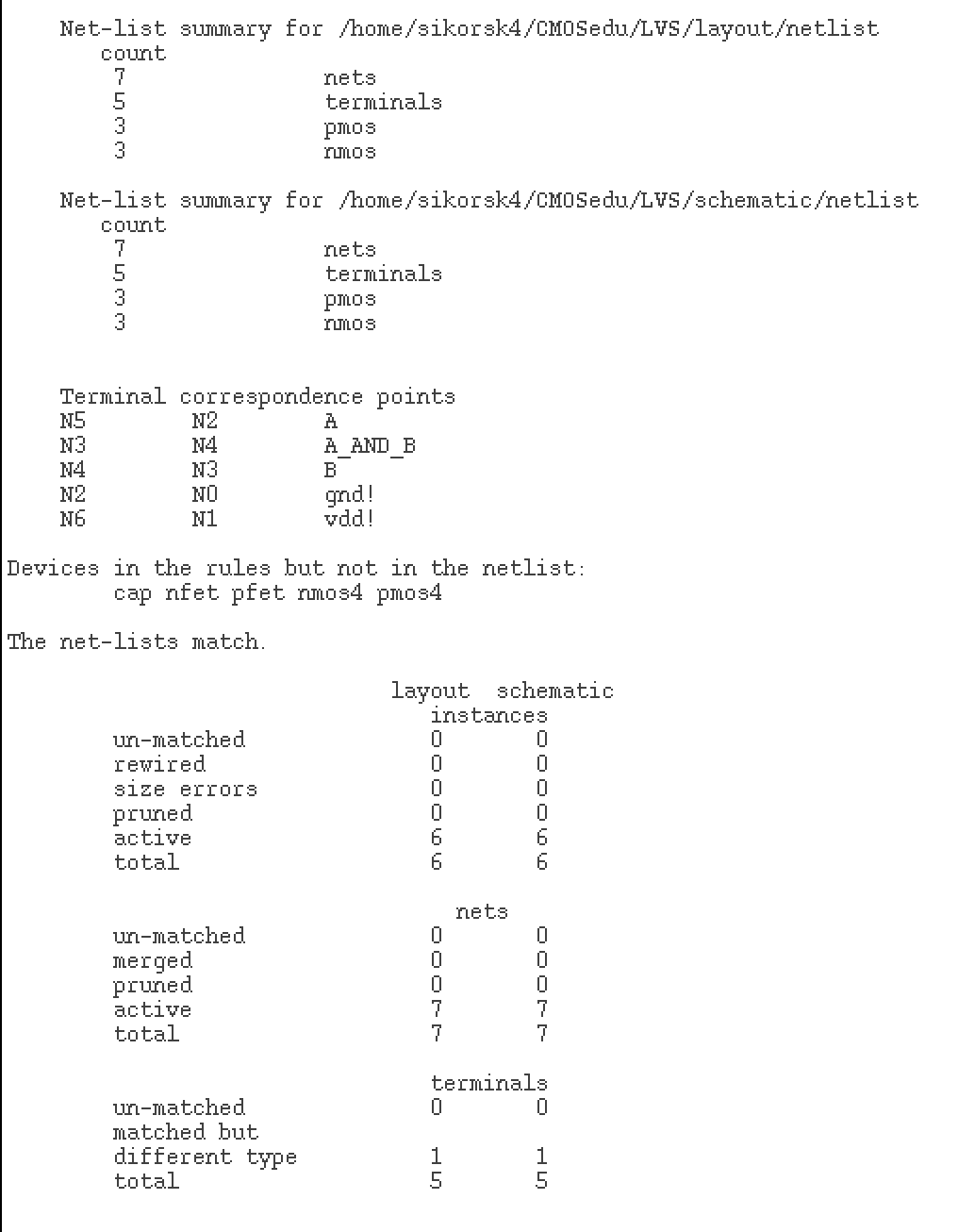
Fig 26
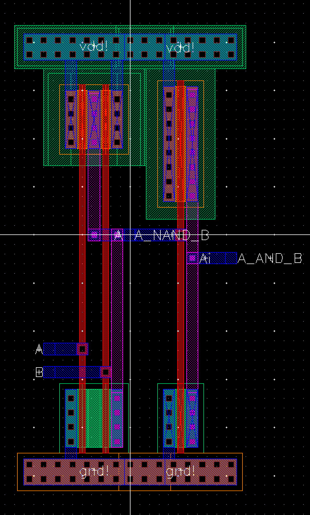
Fig 27

Fig 28
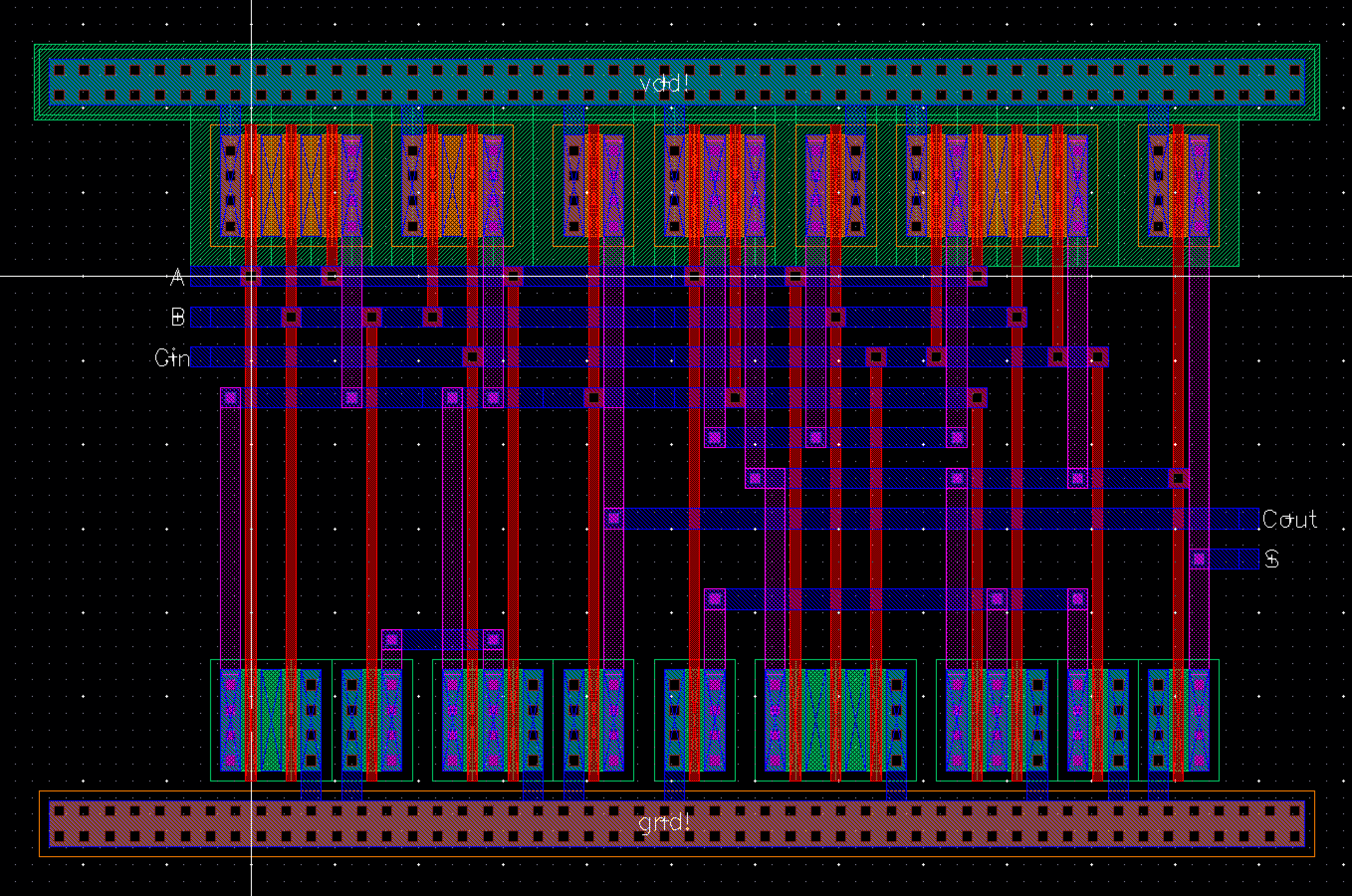
Fig 29
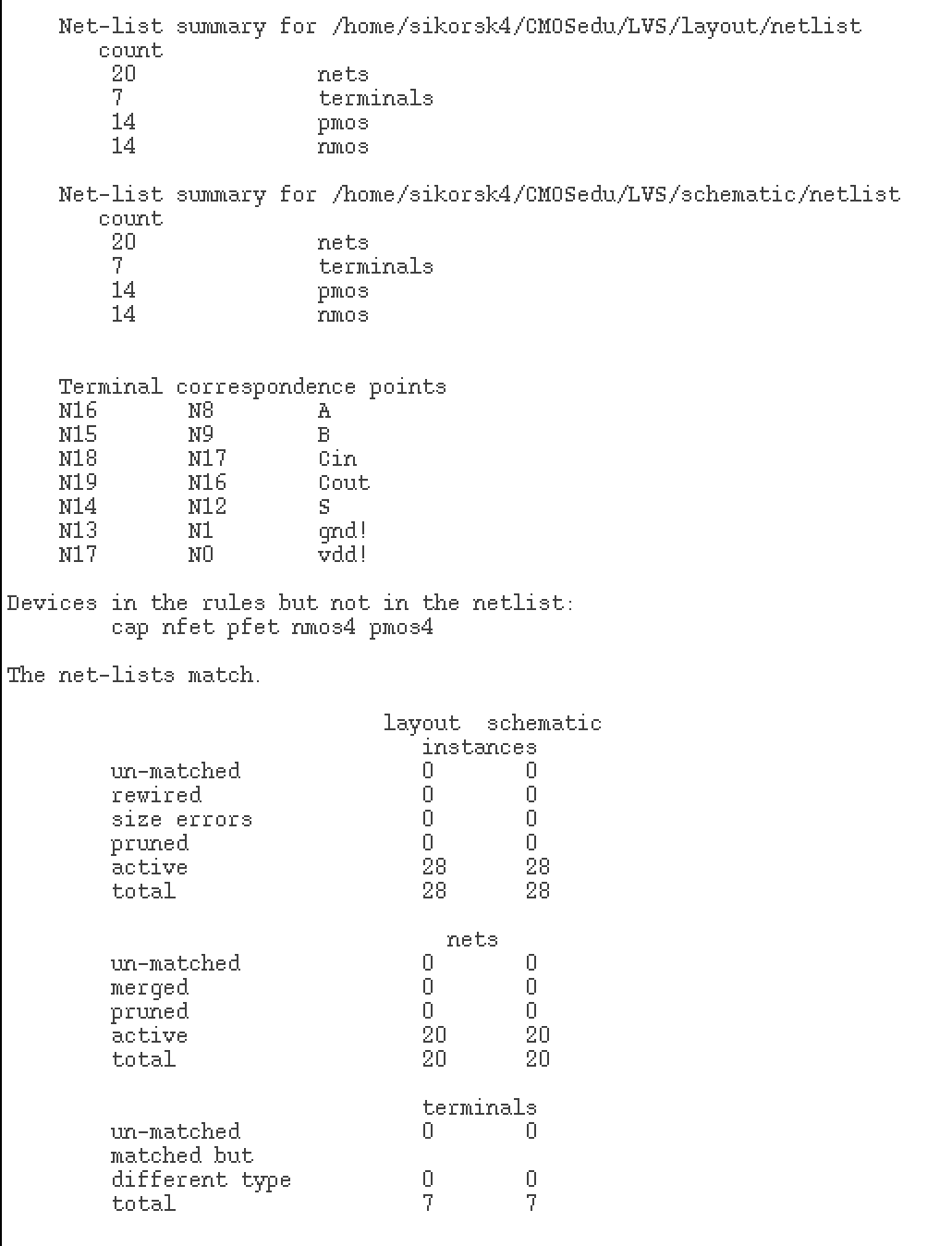
Fig 30

Fig 31
As
mentioned in part 1, a 2 bit XOR gate is needed to perform the
subtraction function. As with the layout for the Full Adder, this one
was also done previously in Lab 6 and will simply need to be refined.
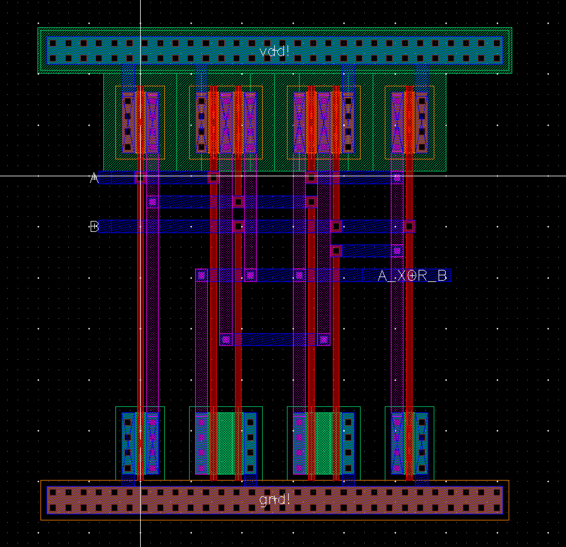 Fig 32 |
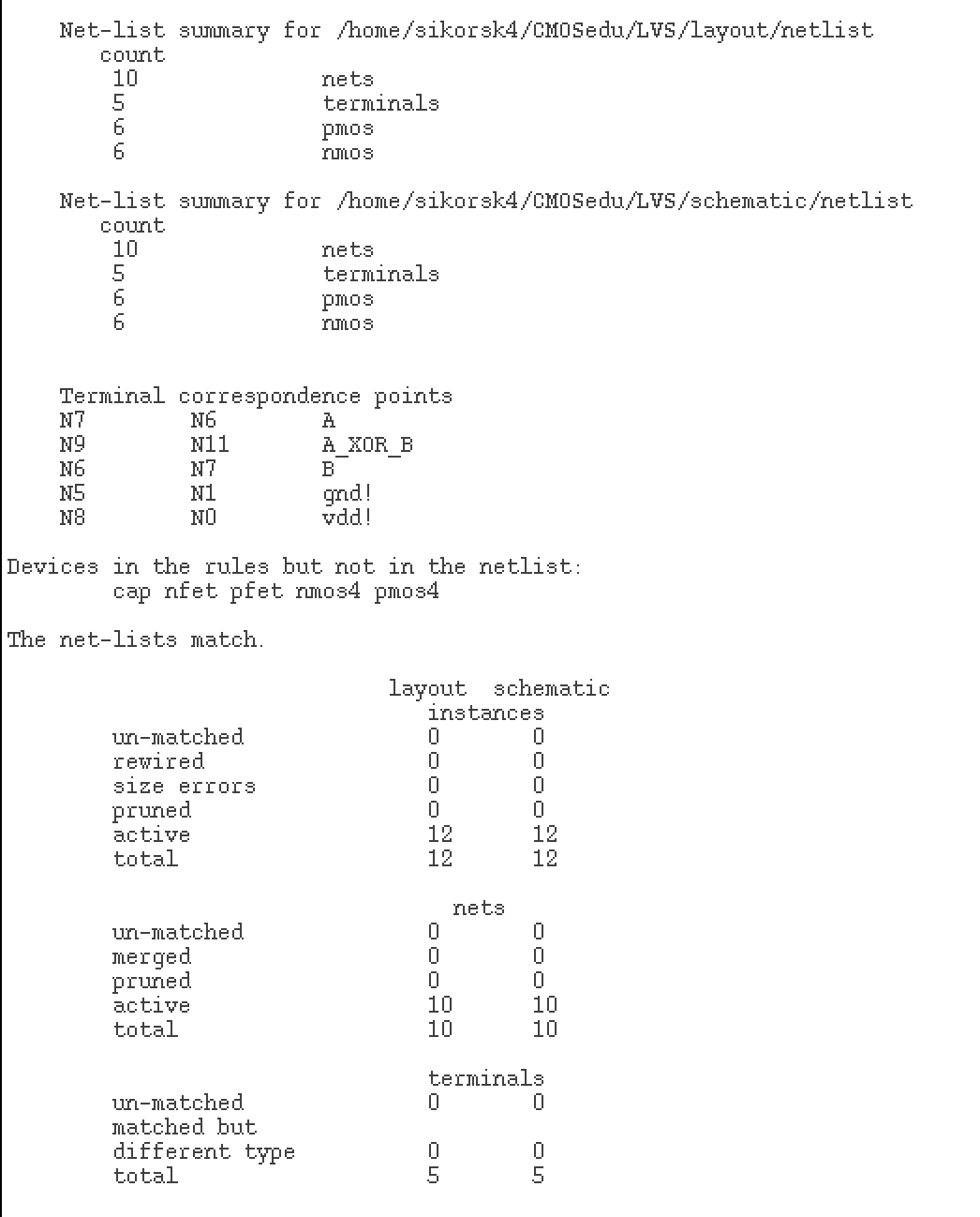 Fig 33 |
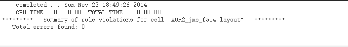 Fig 34 |
The final component of the ALU to be laid out is the 2 bit Multiplexer, again refined from the layout done in Lab 7
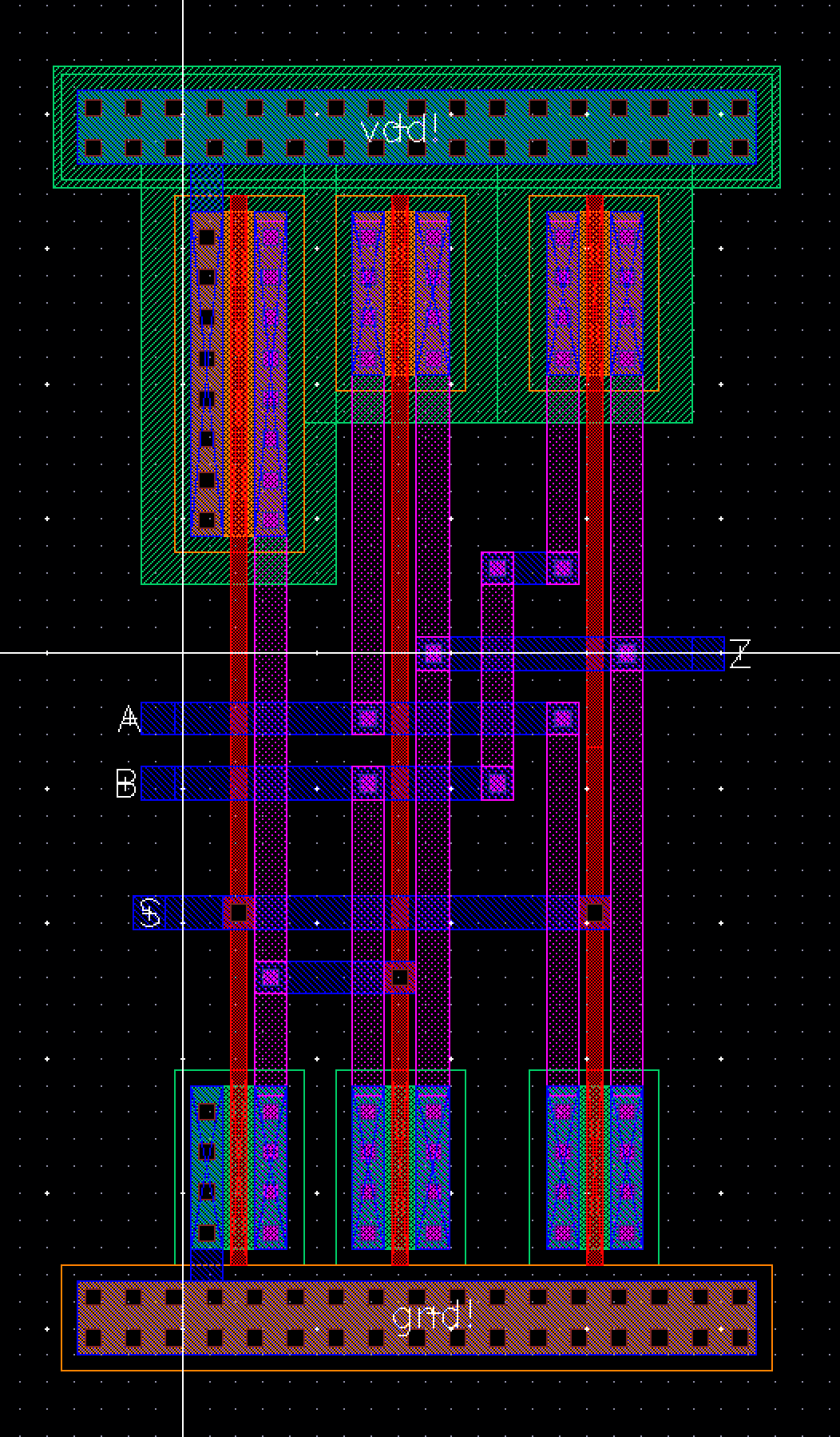 Fig 35 |
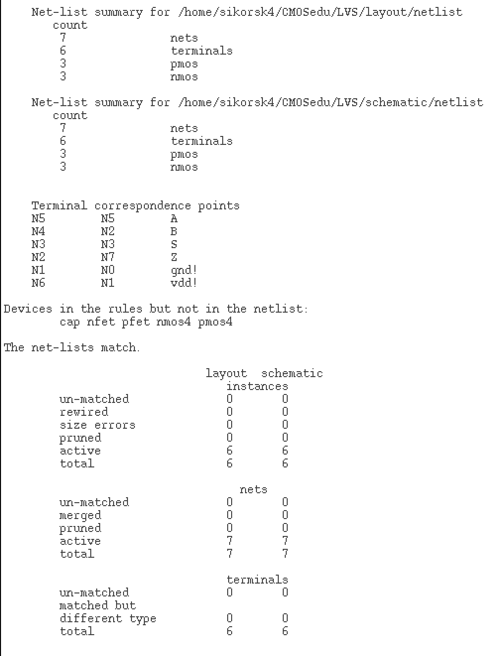 Fig 36 |
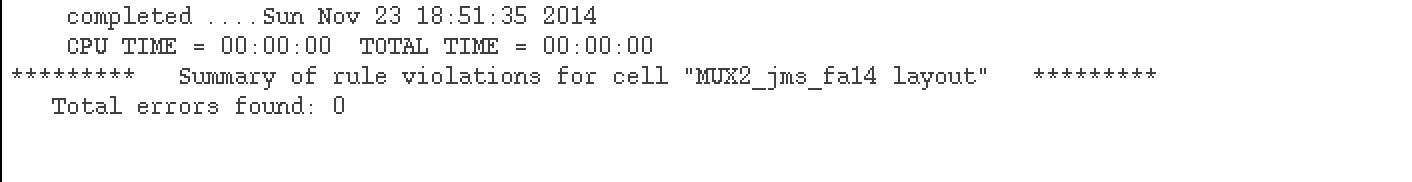 Fig 37 |
Now that all the components have been laid out we can work on the layout for the 8 bit ALU. During the layout of each component special care was given to ensure the space between vdd! and gnd! was equal. This will allow us to align each piece and implement a global gnd and vdd. The gnd and vdd were also extended on the sides of each layout to help facilitate this. For the 8 bit ALU we will start by laying out a 1 bit ALU that can be cascaded together to form the complete 8 bit layout.
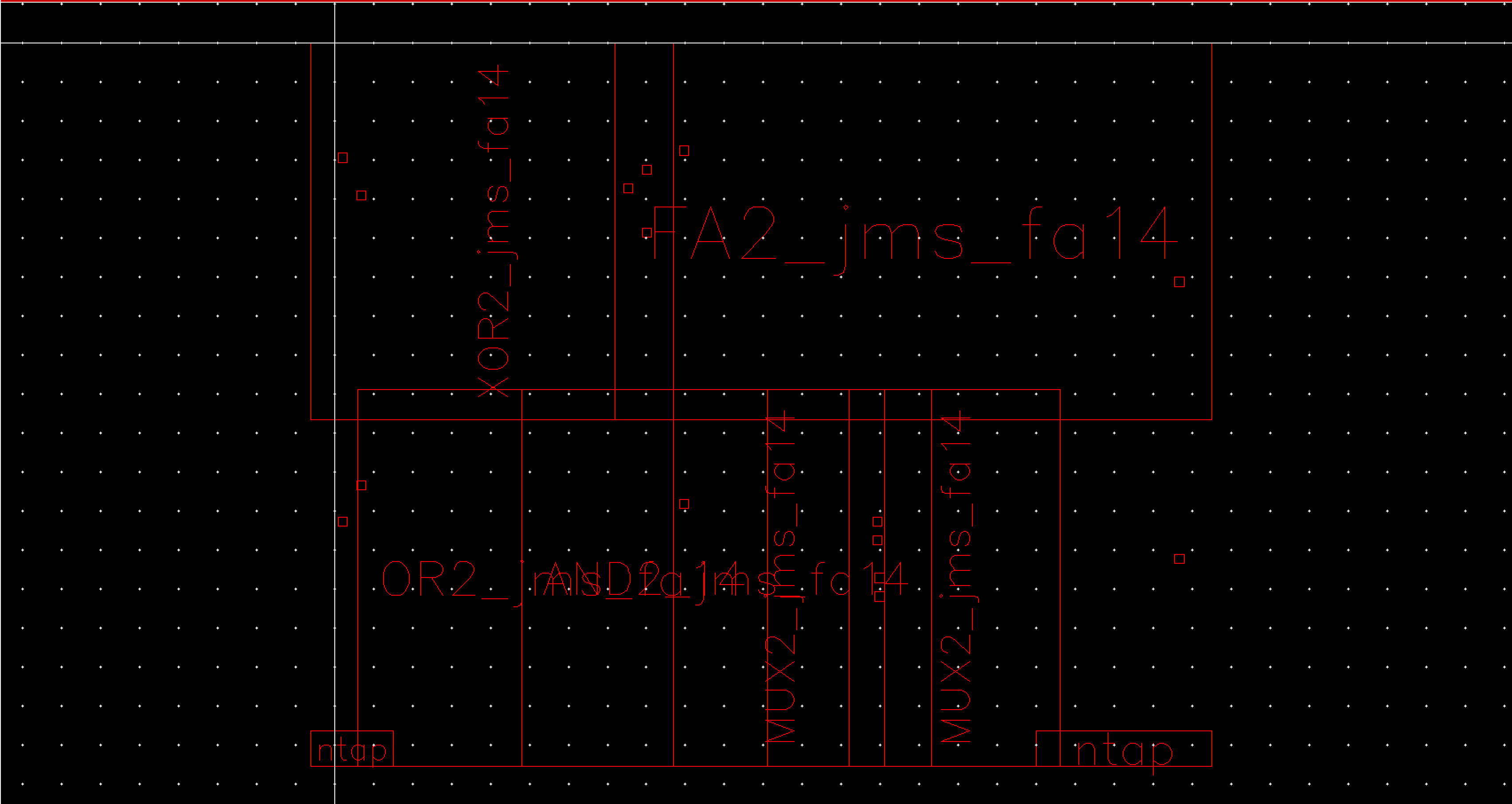 Fig 38 |
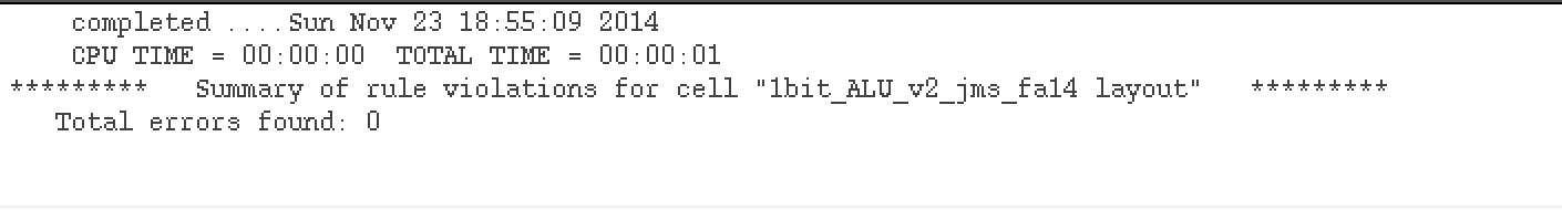 Fig 40 |
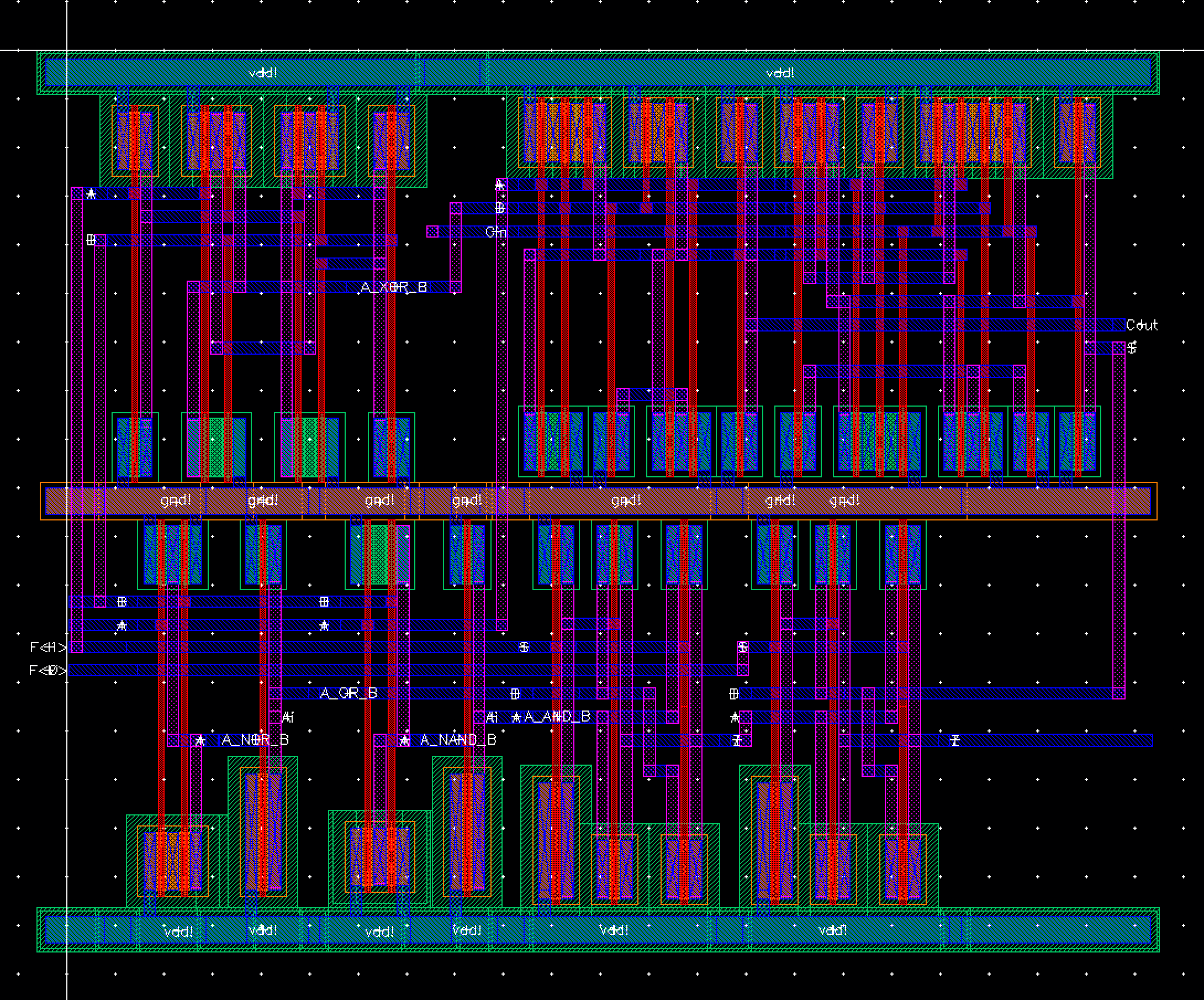 Fig 39 |
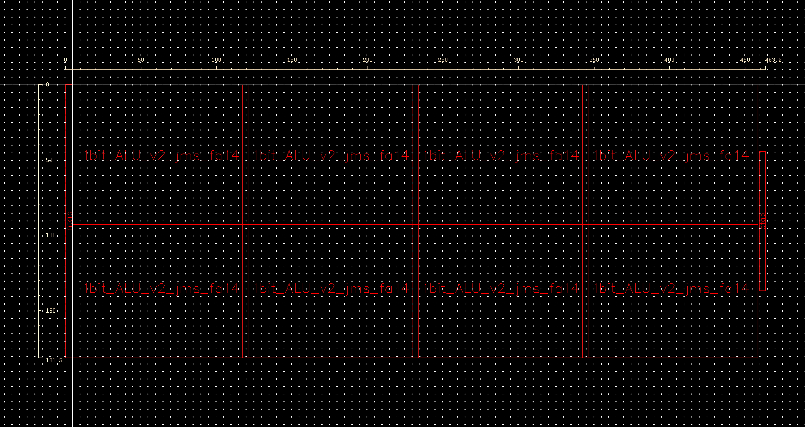
Fig 41
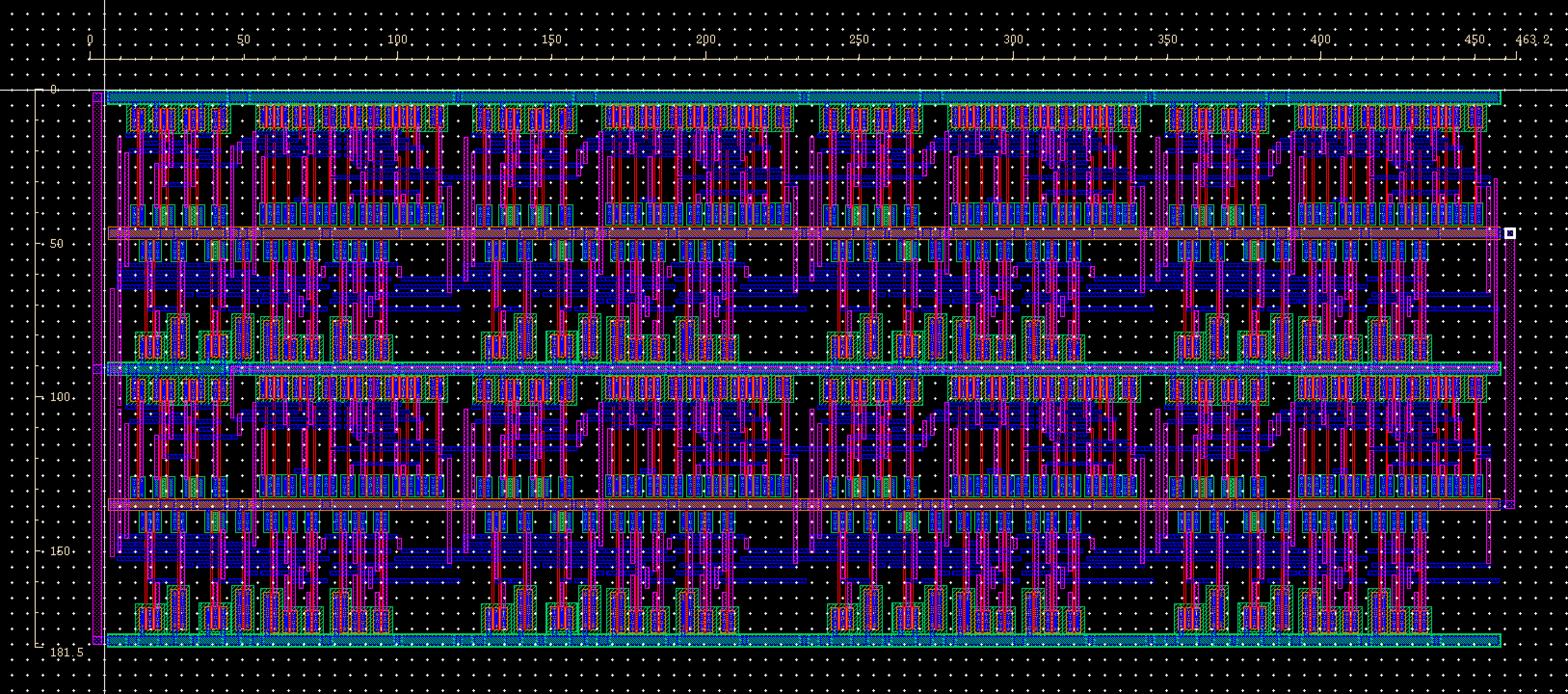
Fig 43
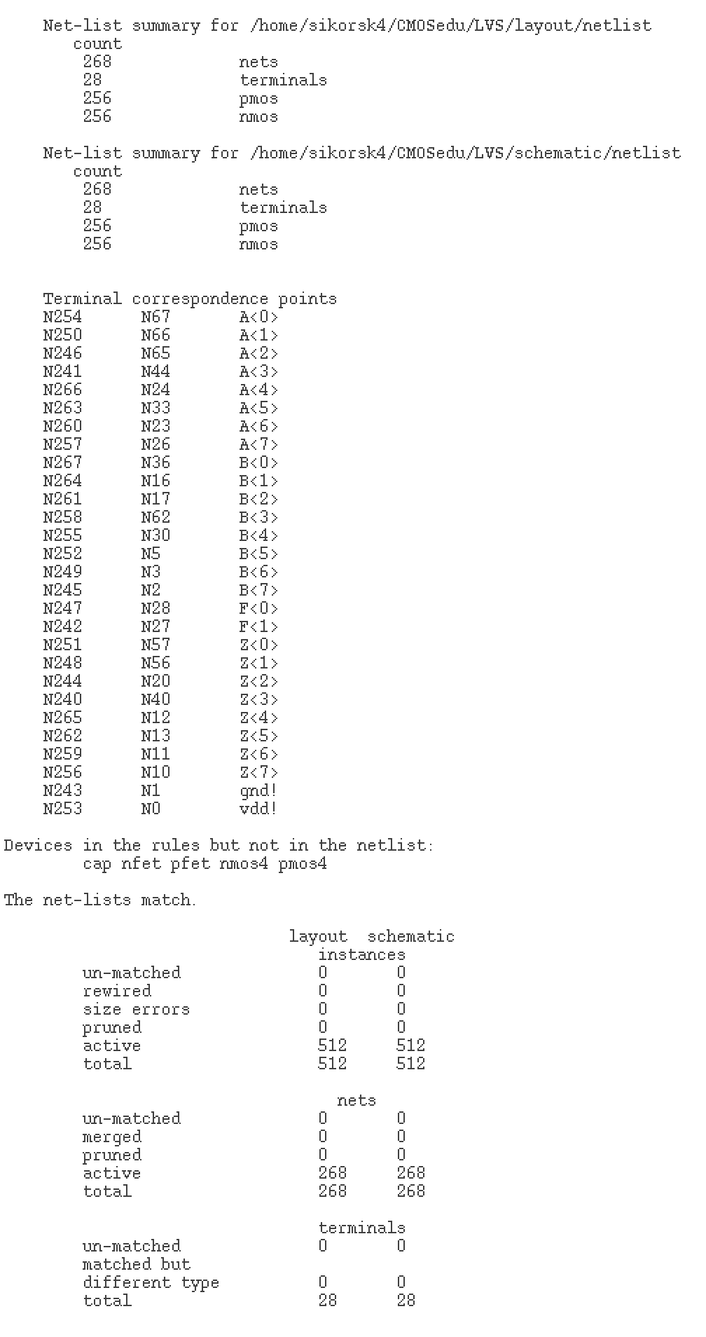
Fig 42
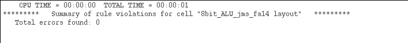
Fig 44
By
having the 1 bit ALU share the same gnd and having a vdd on top and
bottom I was able to cascade each piece into a 2x4 array and then just
connect the 3 vdd runs on the left and the 2 gnd runs on the right. All
inputs are on metal 1. The metal 3 layer was not used, this will allow
all off chip inputs and outputs to utilize this layer without
restriction. The final layout measures 181.5 um by 463.2 um. This
completes both parts of the lab project.
The folder is backed up and zipped.
 Fig 45 |