Lab 6 - ECE 421L
Prepared
by:
PRE-LAB WORK:
Back-up all your work from the lab and the course.
LAB WORK:
For this lab
we will make the layout, schematic and symbol for a NAND gate, XOR gate and a
Full-Adder using these gates. We will use 6u/0.6u PMOS and NMOS transistors for
these designs. To verify the design, simulations will be performed to verify
the truth table.
NAND Gate
Schematic
& Symbol:
|
|
|
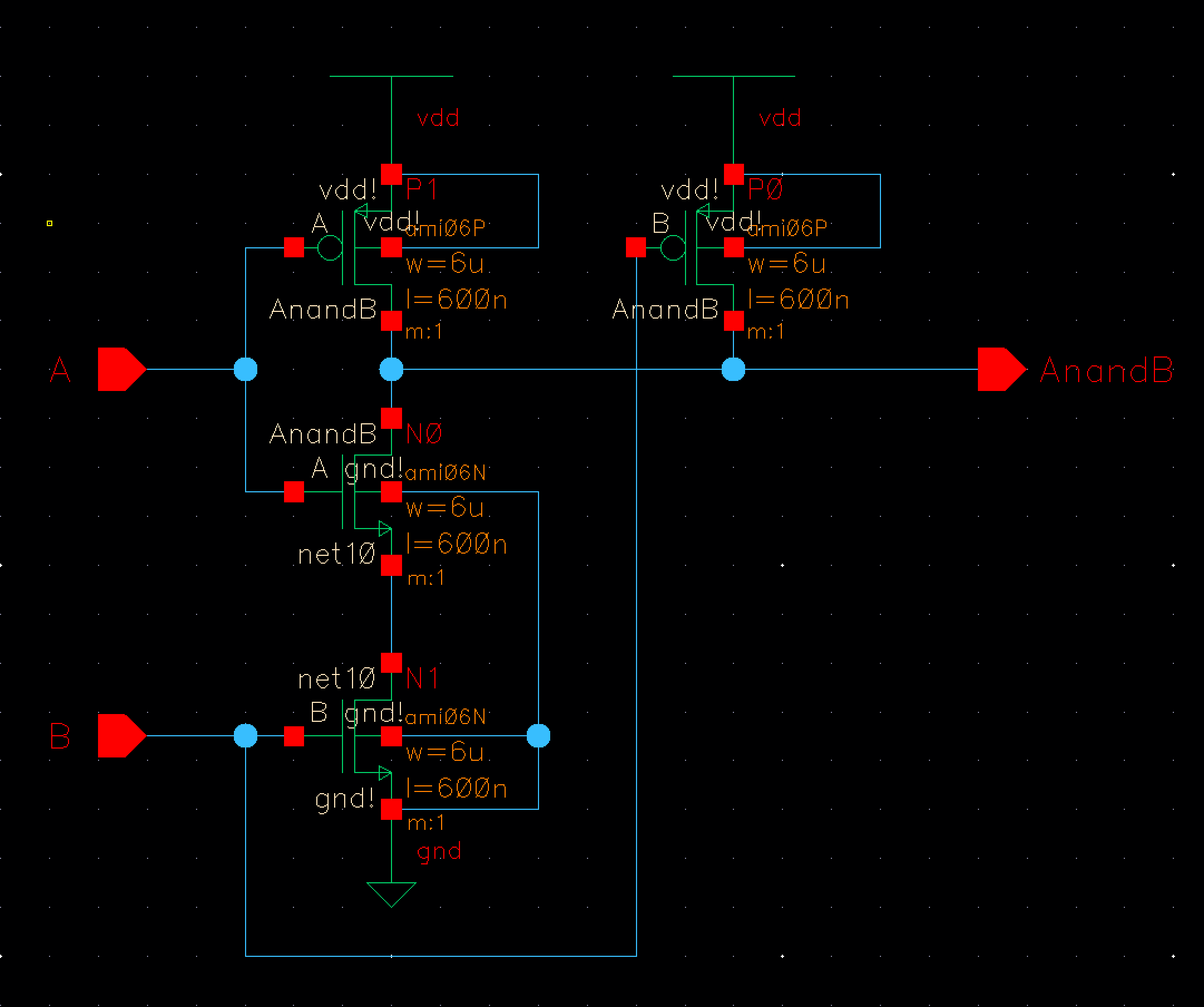 Fig 1
Fig 1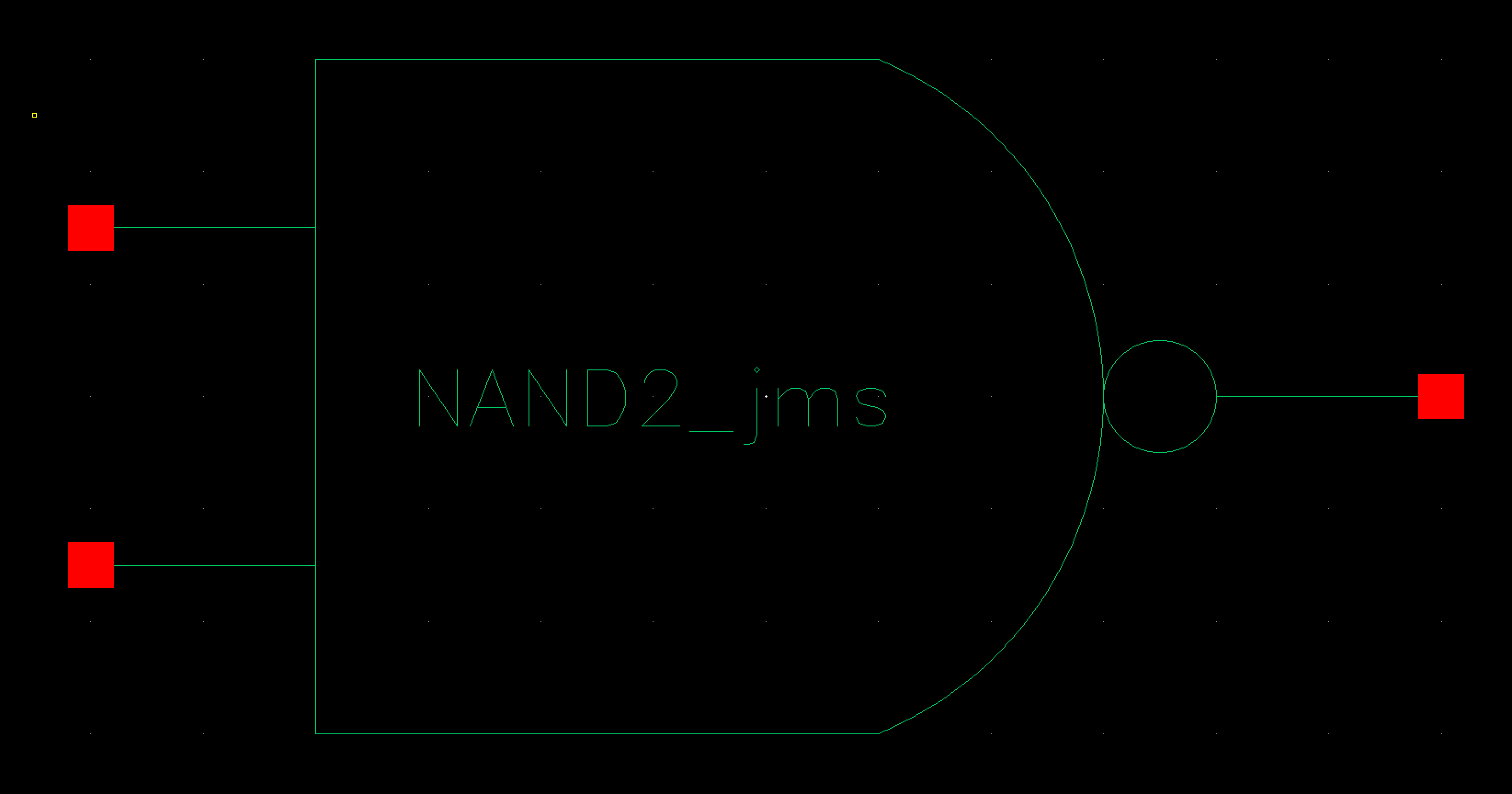 Fig 2
Fig 2For the
symbol design we used the standard symbol.
Layout:
|
Fig 3 |
|
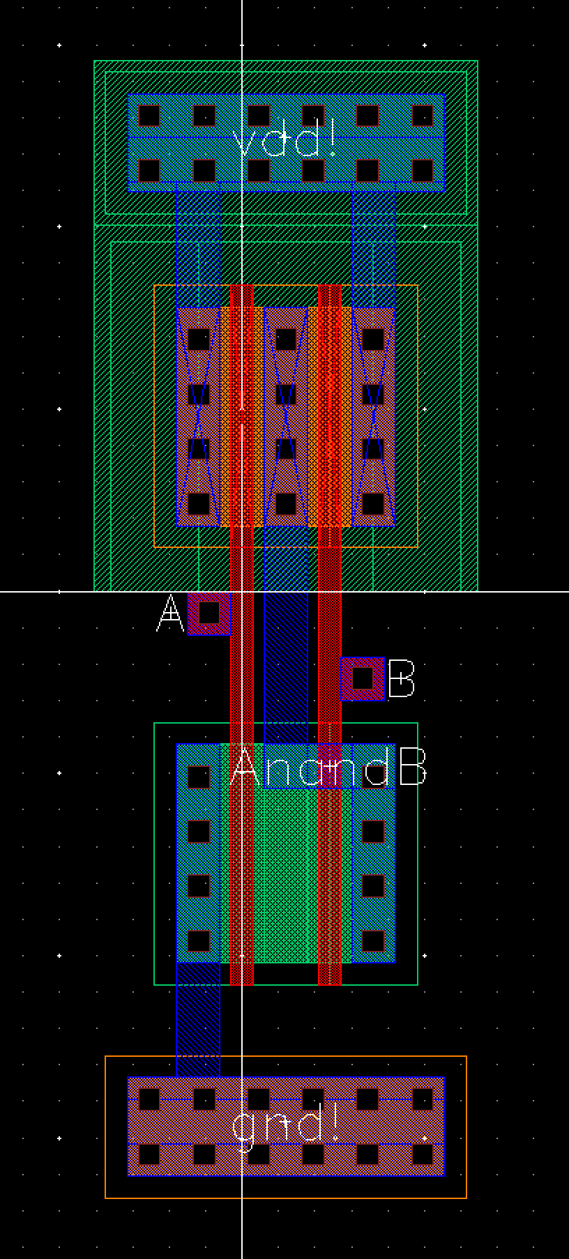
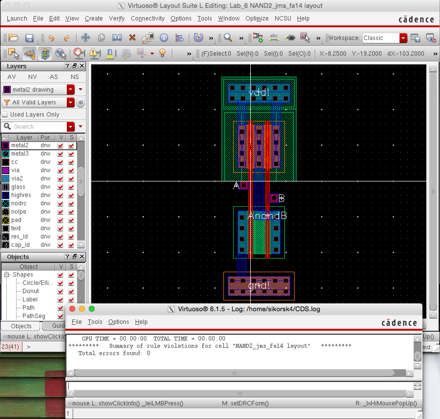 Fig 4
Fig 4A DRC check
was performed and no errors were found. For this layout the A & B inputs as
well as the AnandB output were put on the metal 1 layer.
Extracted
view & LVS:
|
Fig 5 |
|
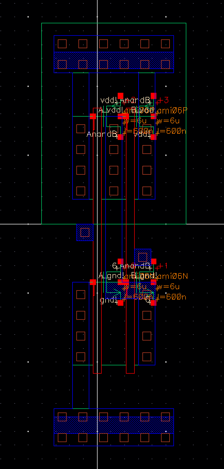
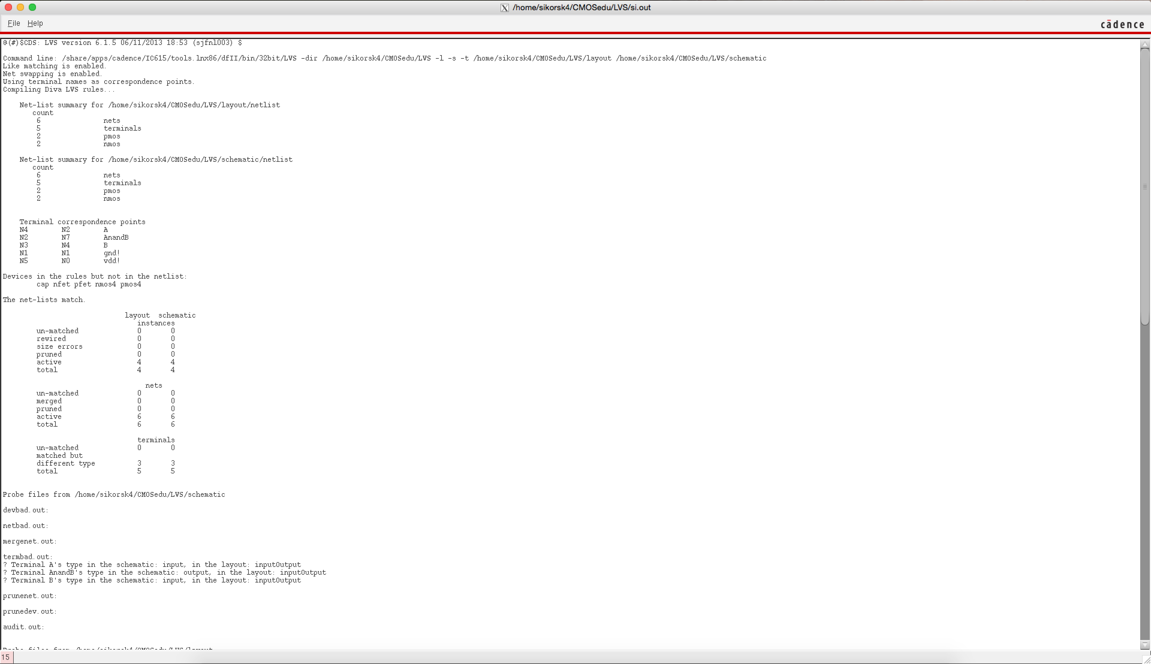 Fig 6
Fig 6The layout
was extracted and an LVS was successfully performed.
XOR GATE
Schematic
& Symbol:
|
|
|
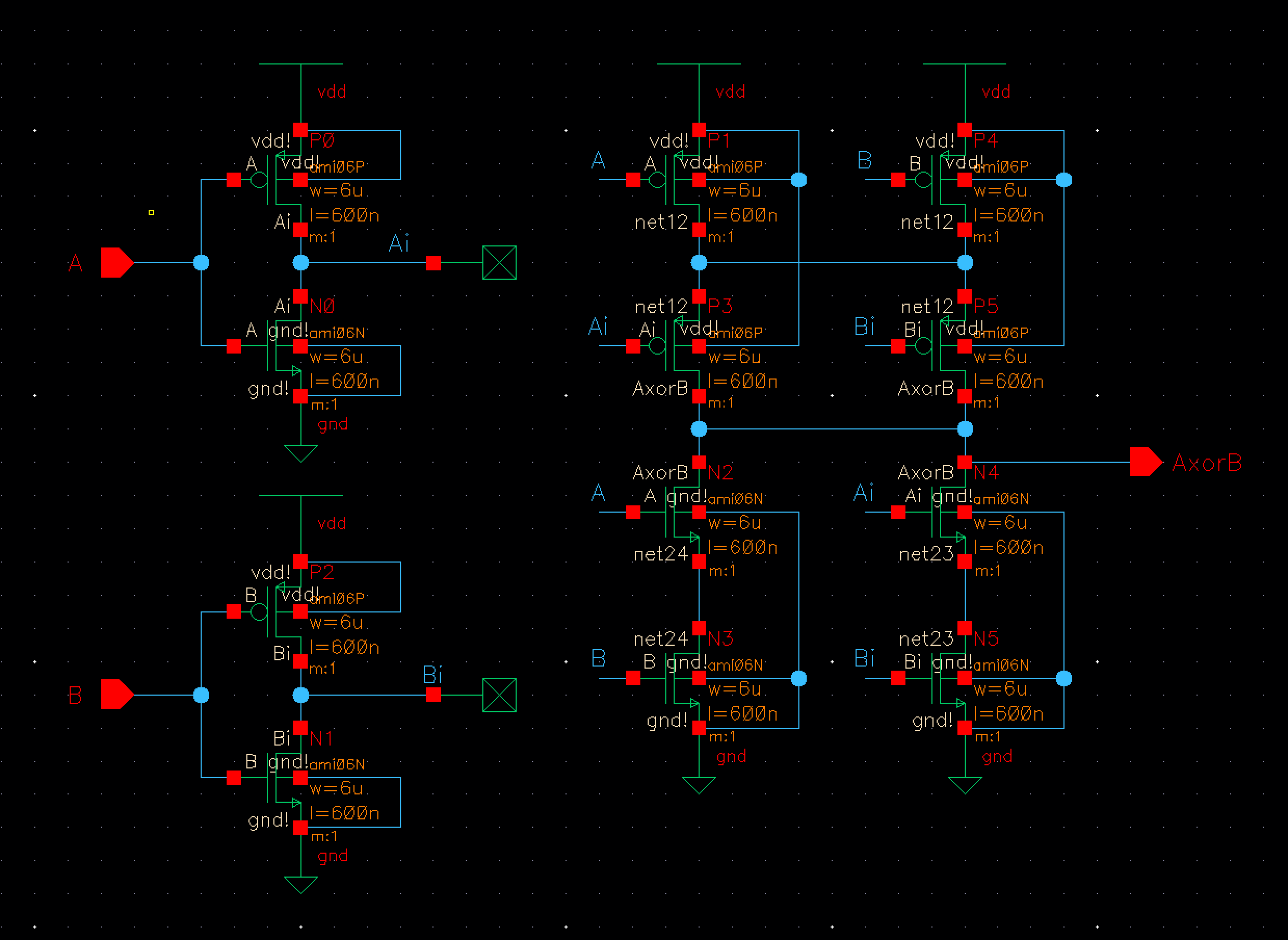 Fig 7
Fig 7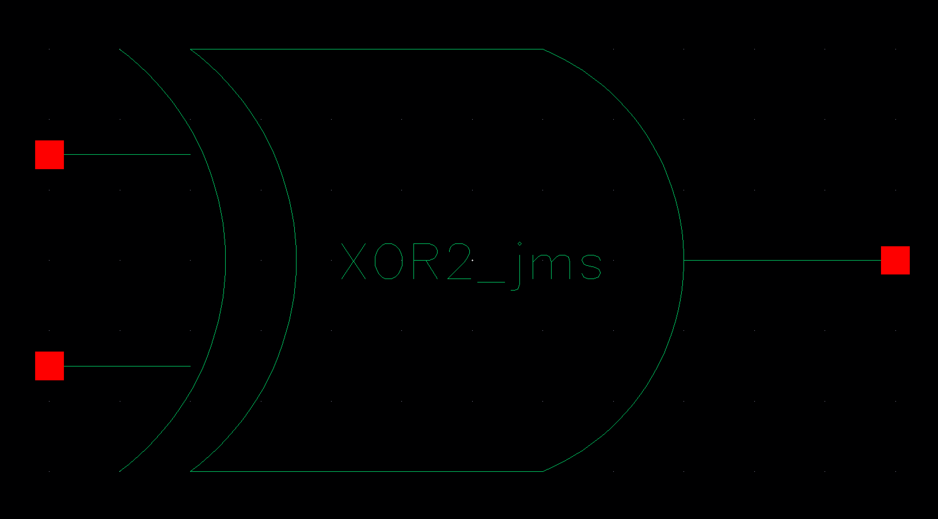 Fig 8
Fig 8 Again the standard XOR symbol was used for
this design.
Layout:
|
|
|
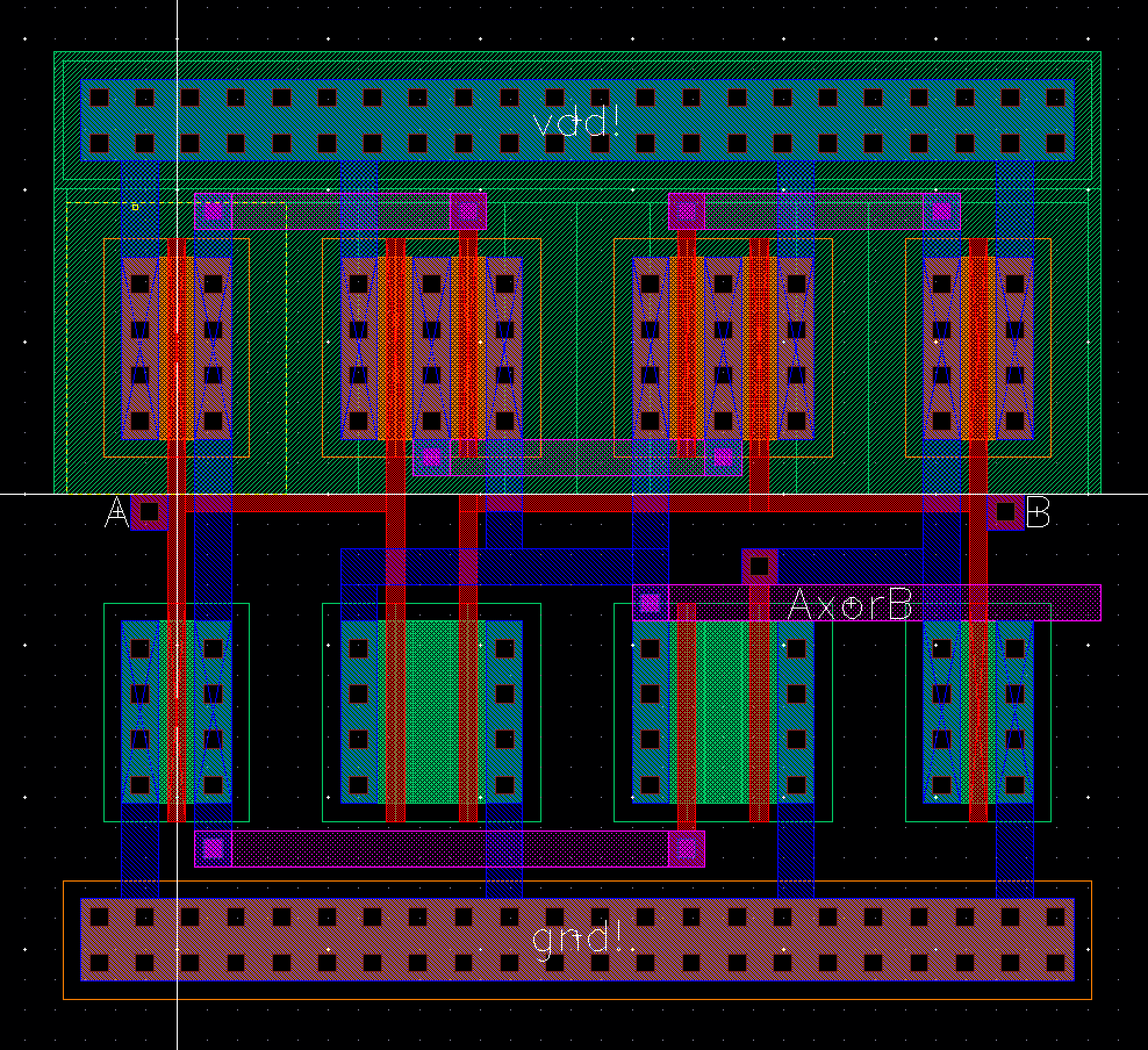 Fig 9
Fig 9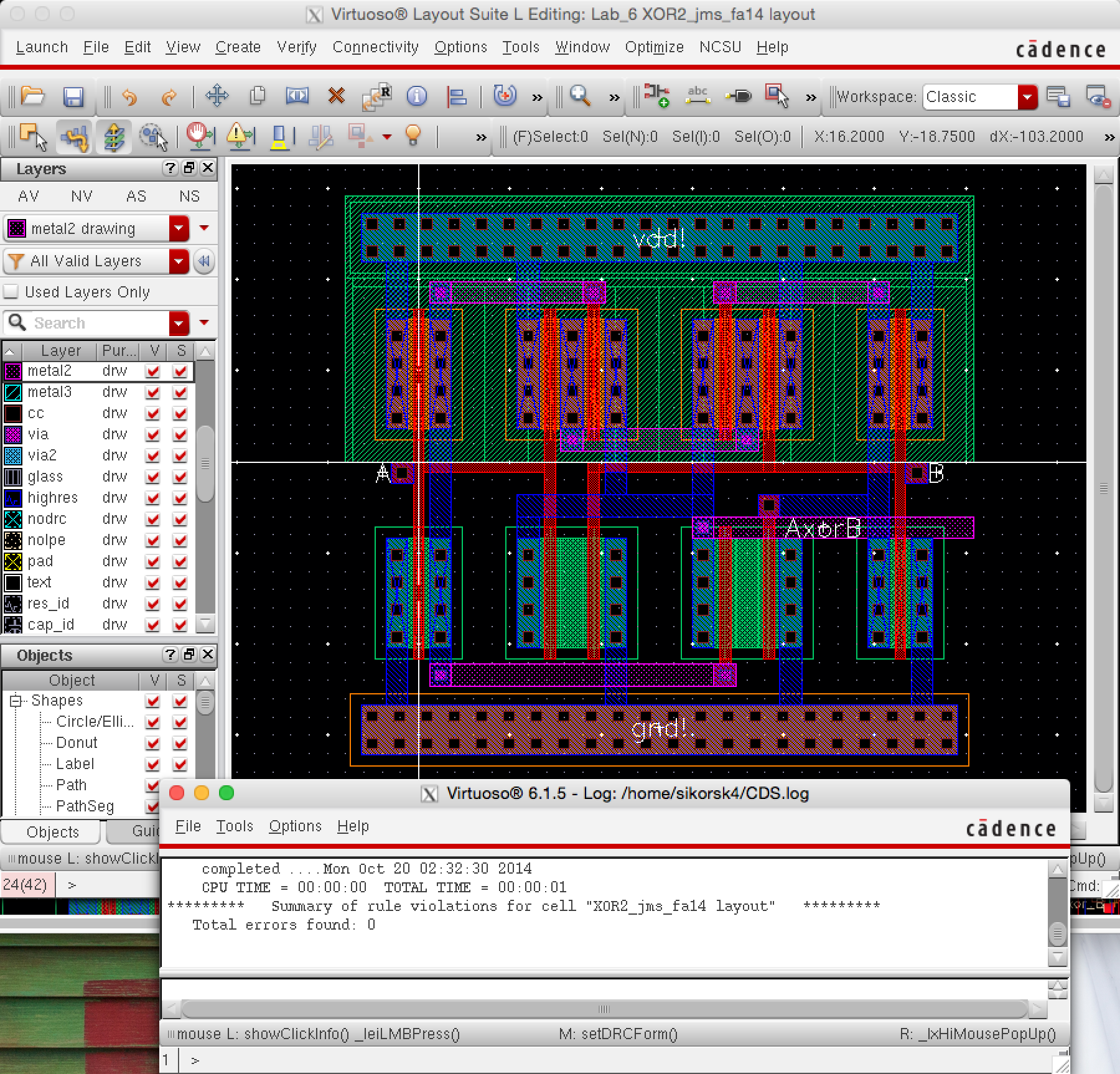 Fig 10
A DRC check
was again performed and no errors were found. For this layout the A & B
inputs are put on metal 1 while the AxorB output is
put on the metal 2 layer. This allowed the output wire to be ran all the way to
the edge of the layout which will be useful in future designs.
Extracted
view & LVS:
|
|
|
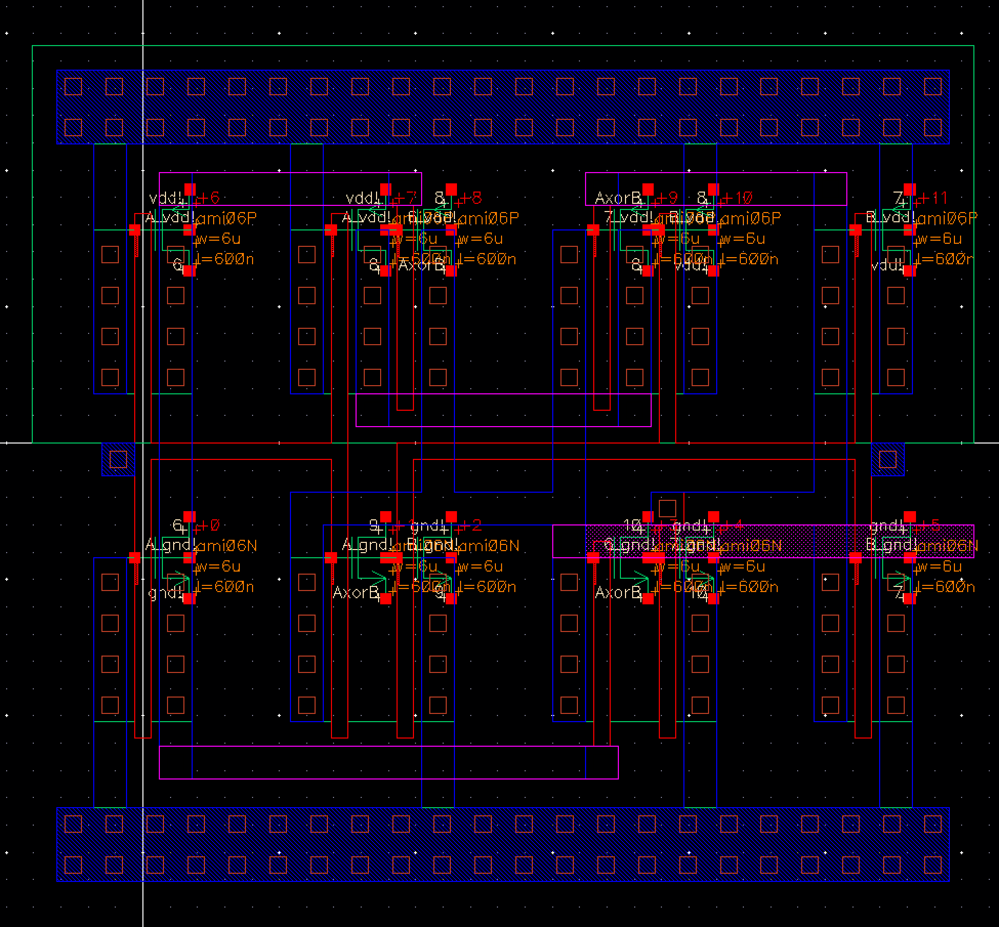 Fig 11
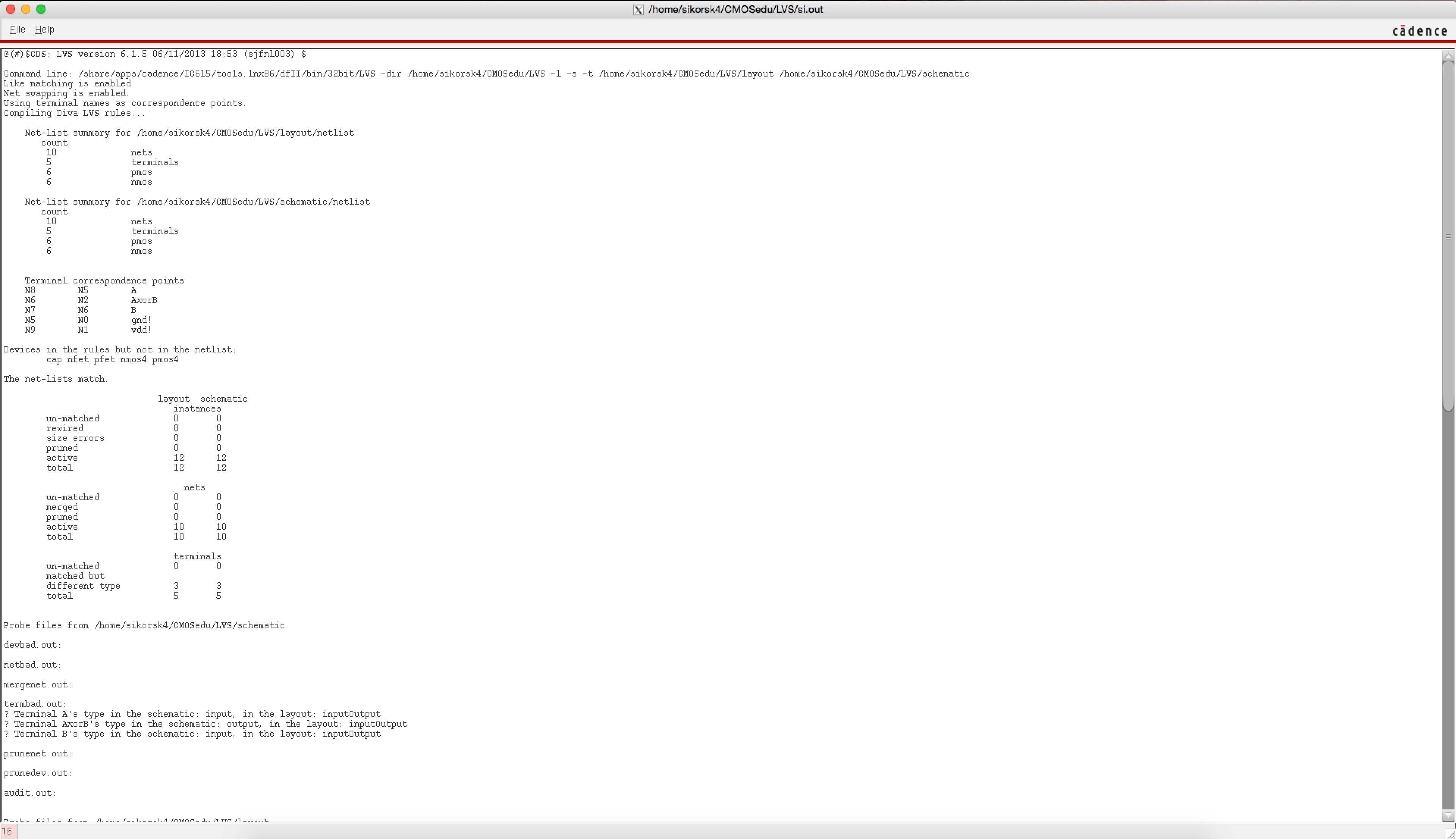 Fig 12
The layout
was extracted and an LVS was successfully performed.
Now that
both gates have been successfully designed it is time to ensure they perform as
expected. To do this a simulation with all possible inputs will be performed.
NAND & XOR Simulation
For this
simulation we will also use the inverter
from lab 5 to verify the input.
Truth Table:
|
A |
0 |
0 |
1 |
1 |
|
B |
0 |
1 |
0 |
1 |
|
A' |
1 |
1 |
0 |
0 |
|
AnandB |
1 |
1 |
1 |
0 |
|
AXORB |
0 |
1 |
1 |
0 |
Schematic:
|
|
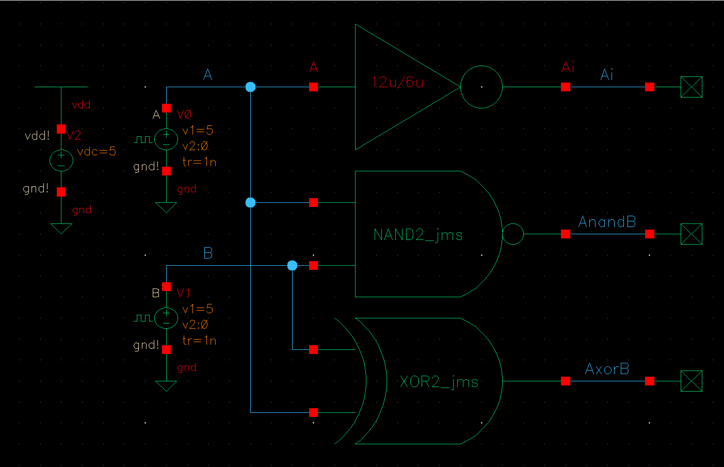 Fig 13
Simulation:
|
|
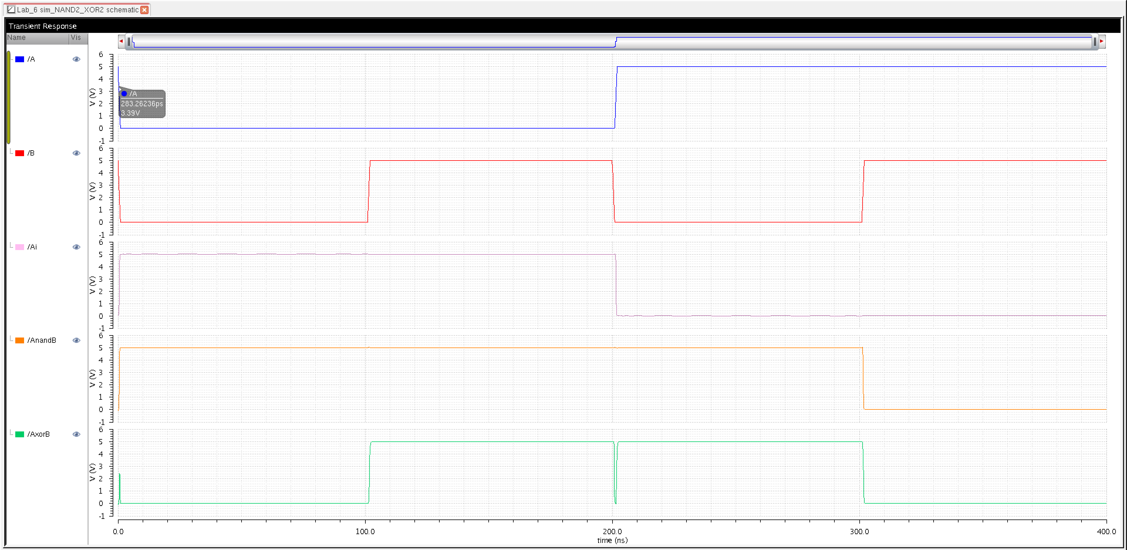 Fig 14
Here we see
that our simulation matched the expected results. However we also see that at t
= 200ns the output of AxorB quickly drops from 1 to 0
and back to 1. This is due to A and B changing at the same time causing a false
result. This false result could cause momentary glitches and should be taken
into consideration when these gates are used for more complex design.
Full-Adder
Now that we
have verified the logic operation of our gates we will use them to implement a
Full-Adder.
Schematic & Symbol:
|
|
|
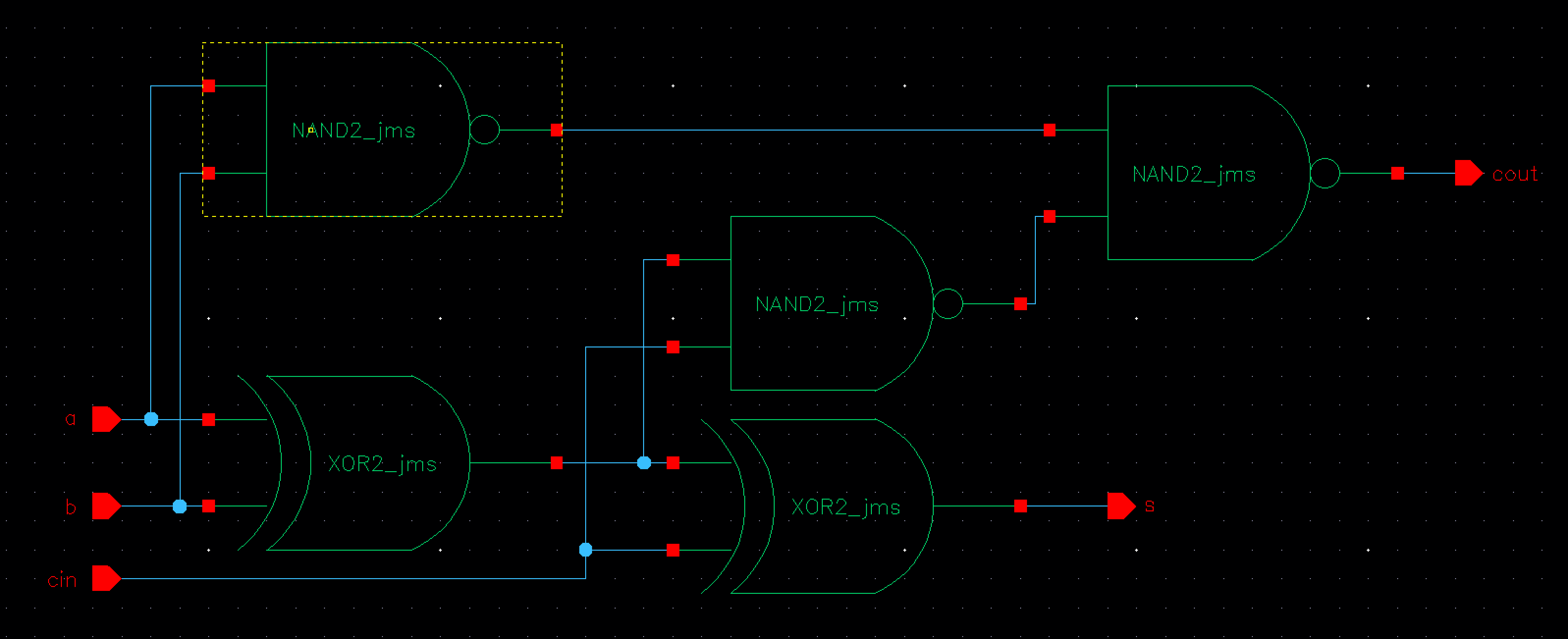 Fig 15
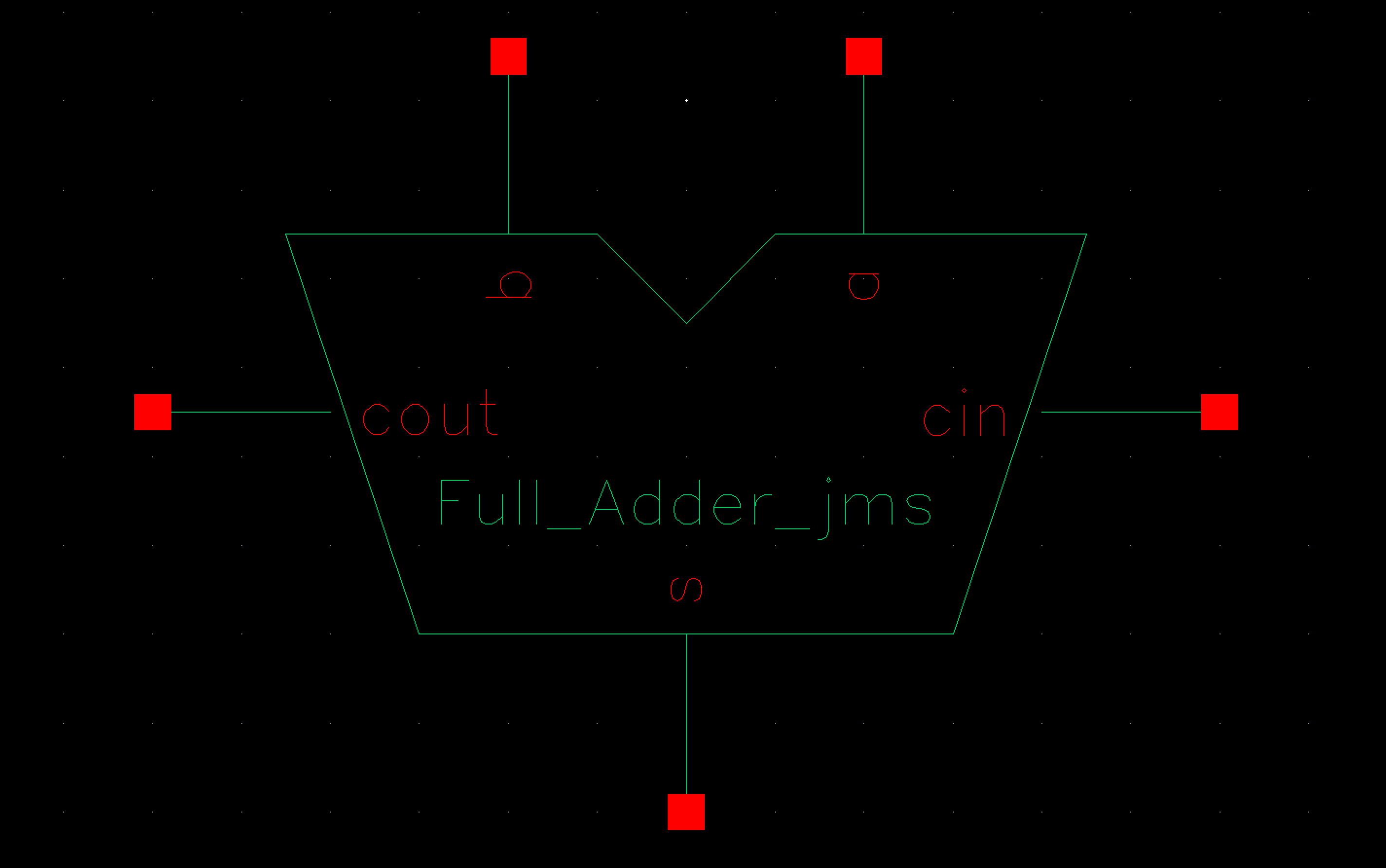 Fig 16
For the
schematic we used the symbols from our gate design. By using the standard
symbol when we did those designs this schematic is considerably easier to
understand.
Layout:
|
|
|
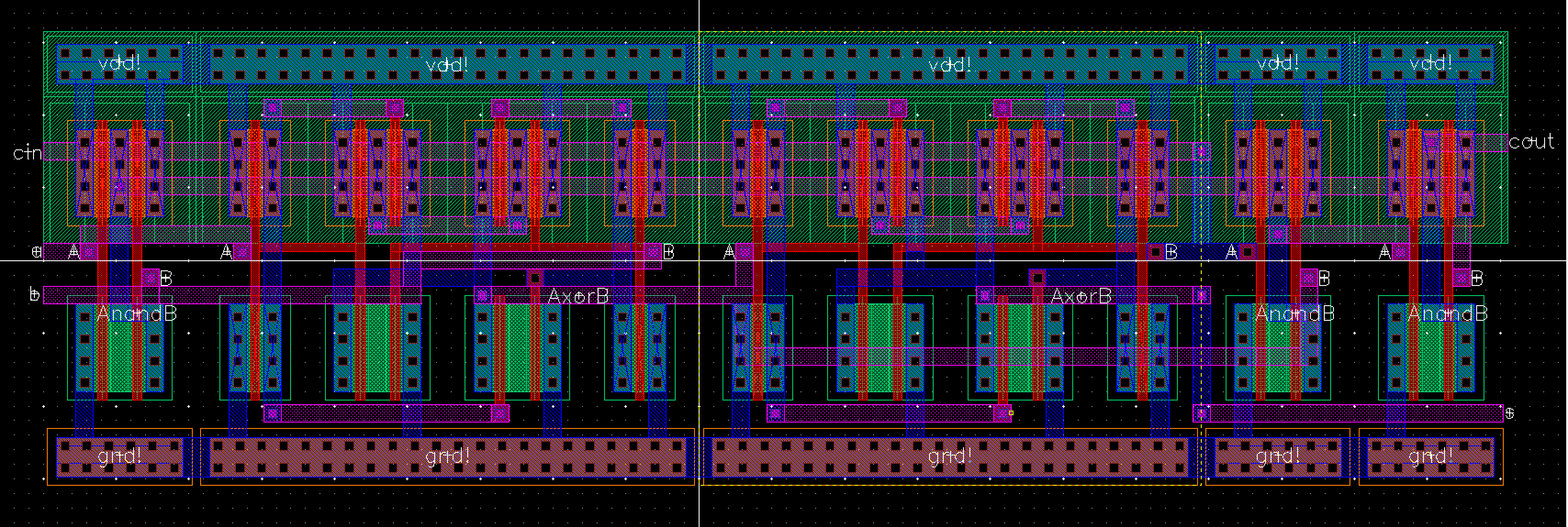 Fig 17
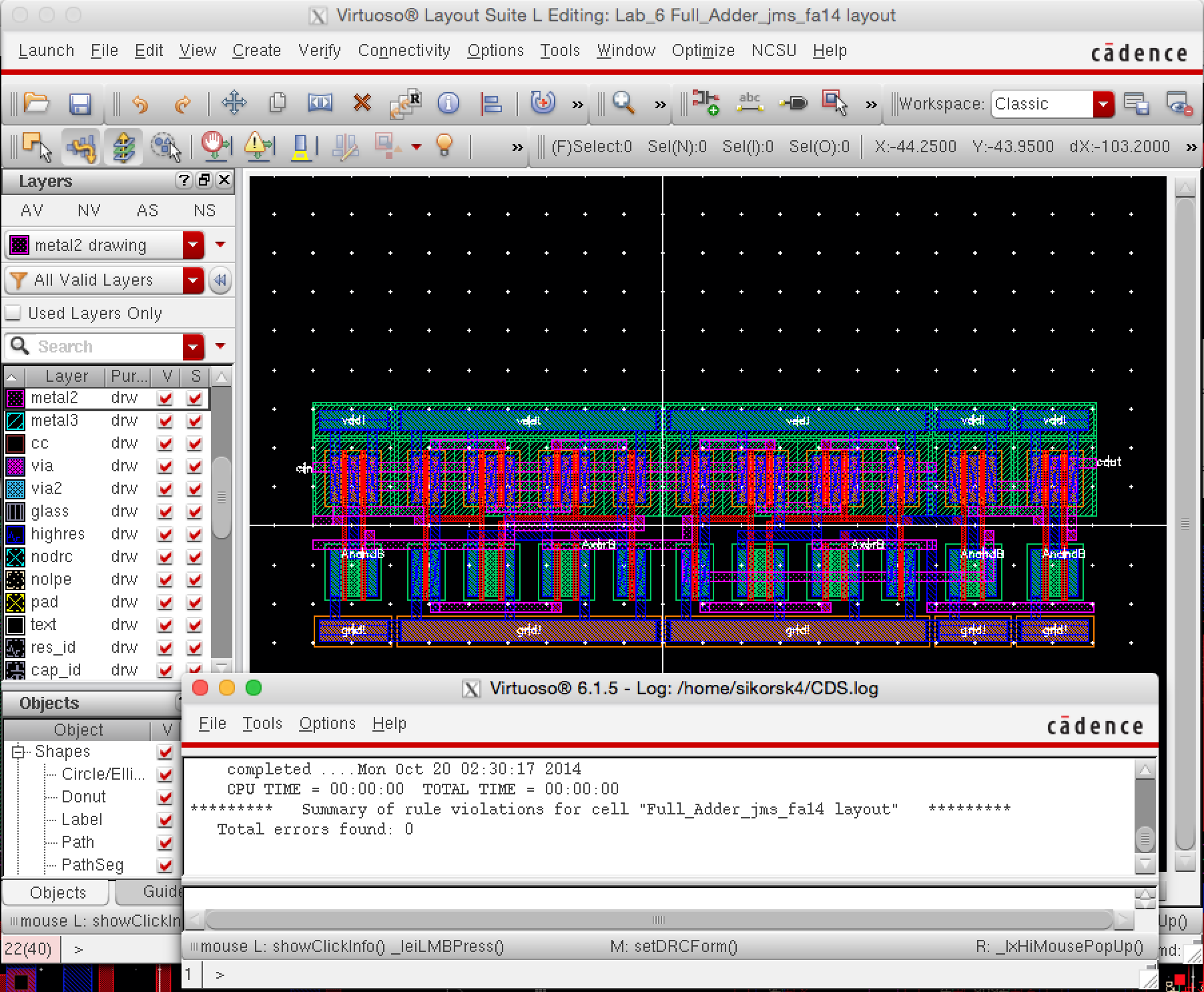 Fig 18
A DRC check
was performed and no errors were found. For this layout the a,
b, and cin inputs as well as the s and cout outputs are all put on the metal 2 layer. For this
design it was important to be careful with spacing of the metal runs. Because
of this we ensured that all inputs and outputs reach the edge of the layout,
this will ensure that future implementation of this design will be simple to
connect.
Extracted
view & LVS:
|
|
|
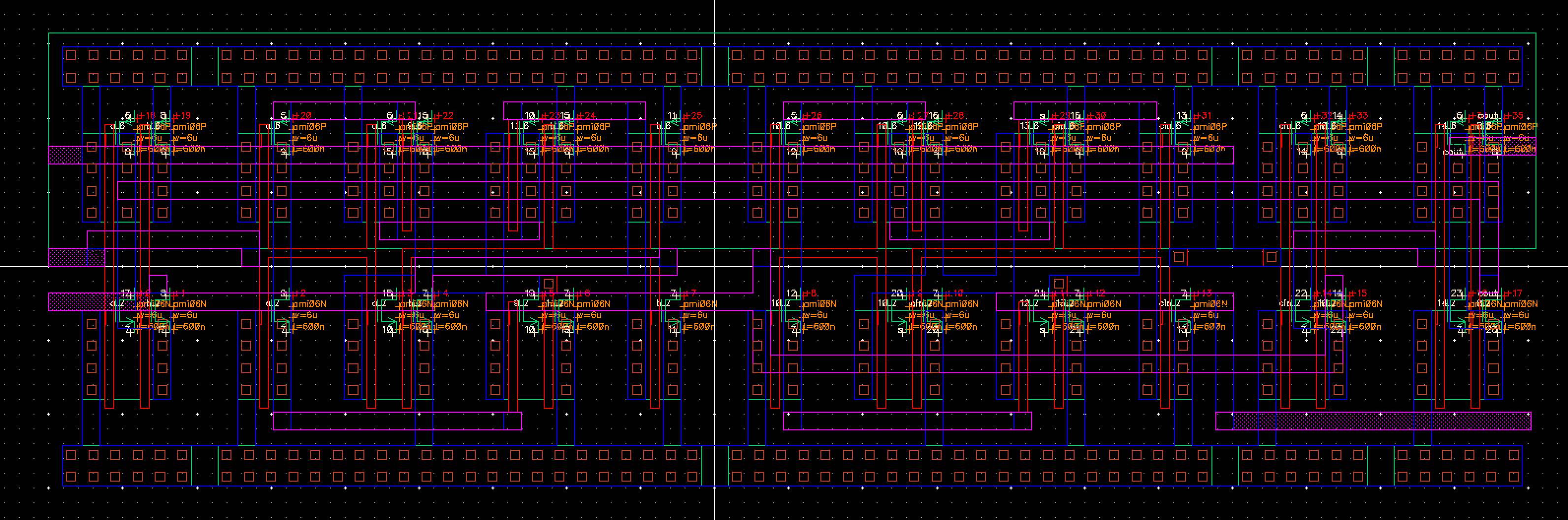 Fig 19
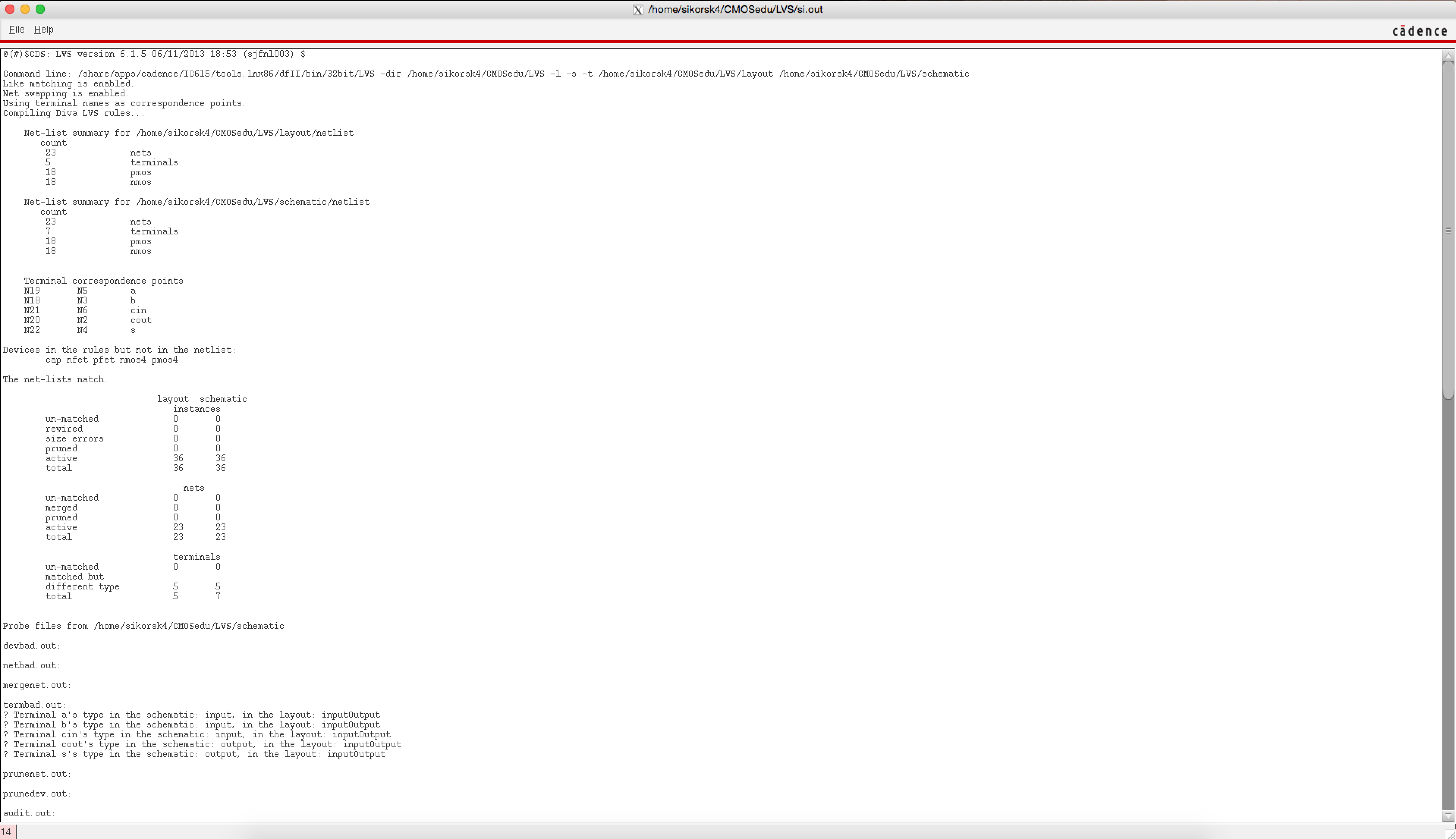 Fig 20
The layout
was extracted and an LVS was successfully performed.
Now that the
Full-Adder is complete we need to run a simulation to ensure our results match
the expected output.
Full-Adder Simulation
Truth Table:
|
A |
0 |
0 |
0 |
0 |
1 |
1 |
1 |
1 |
|
B |
0 |
0 |
1 |
1 |
0 |
0 |
1 |
1 |
|
Cin |
0 |
1 |
0 |
1 |
0 |
1 |
0 |
1 |
|
Cout |
0 |
0 |
0 |
1 |
0 |
1 |
1 |
1 |
|
S |
0 |
1 |
1 |
0 |
1 |
0 |
0 |
1 |
Schematic:
|
|
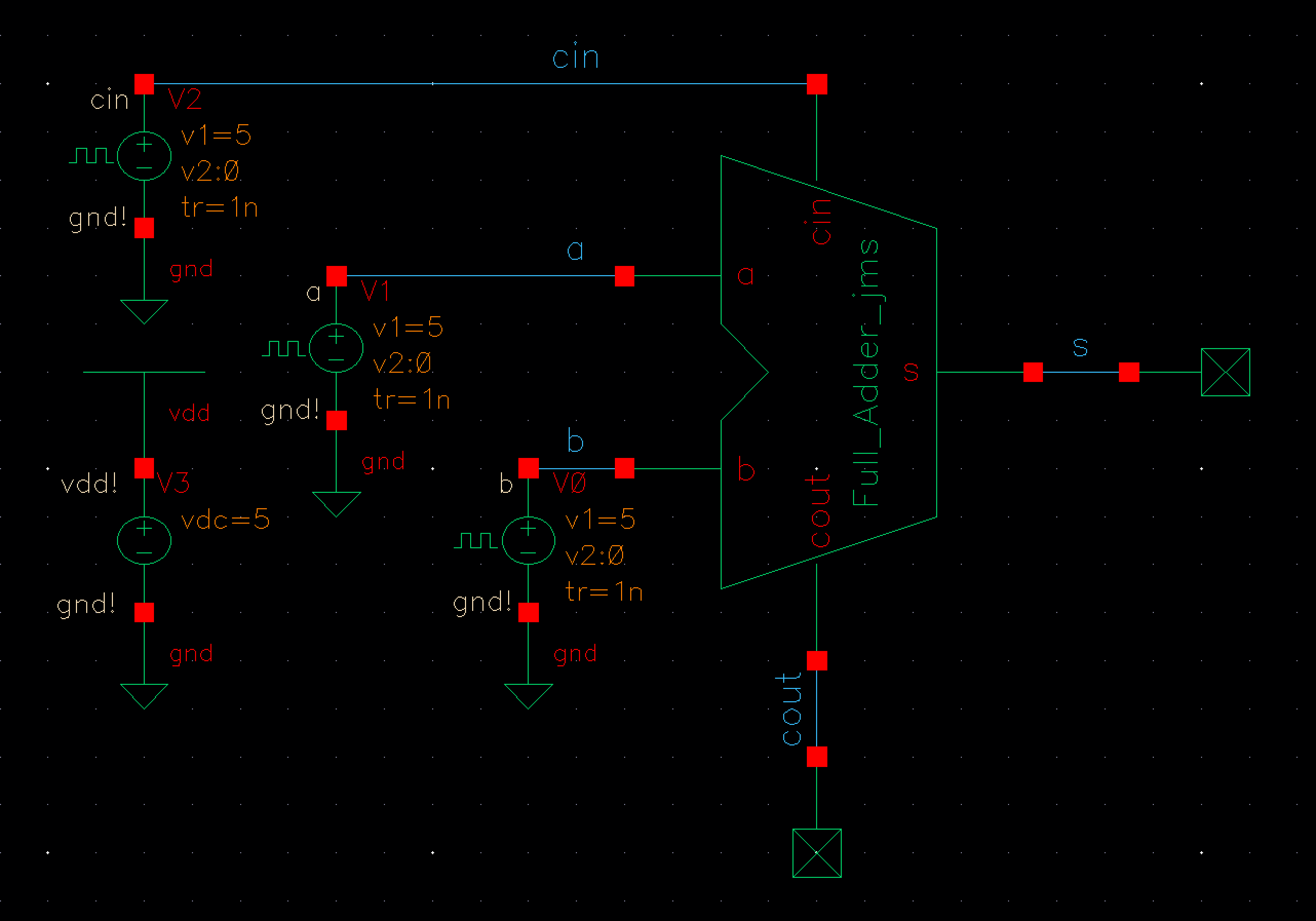 Fig 21
Simulation:
|
|
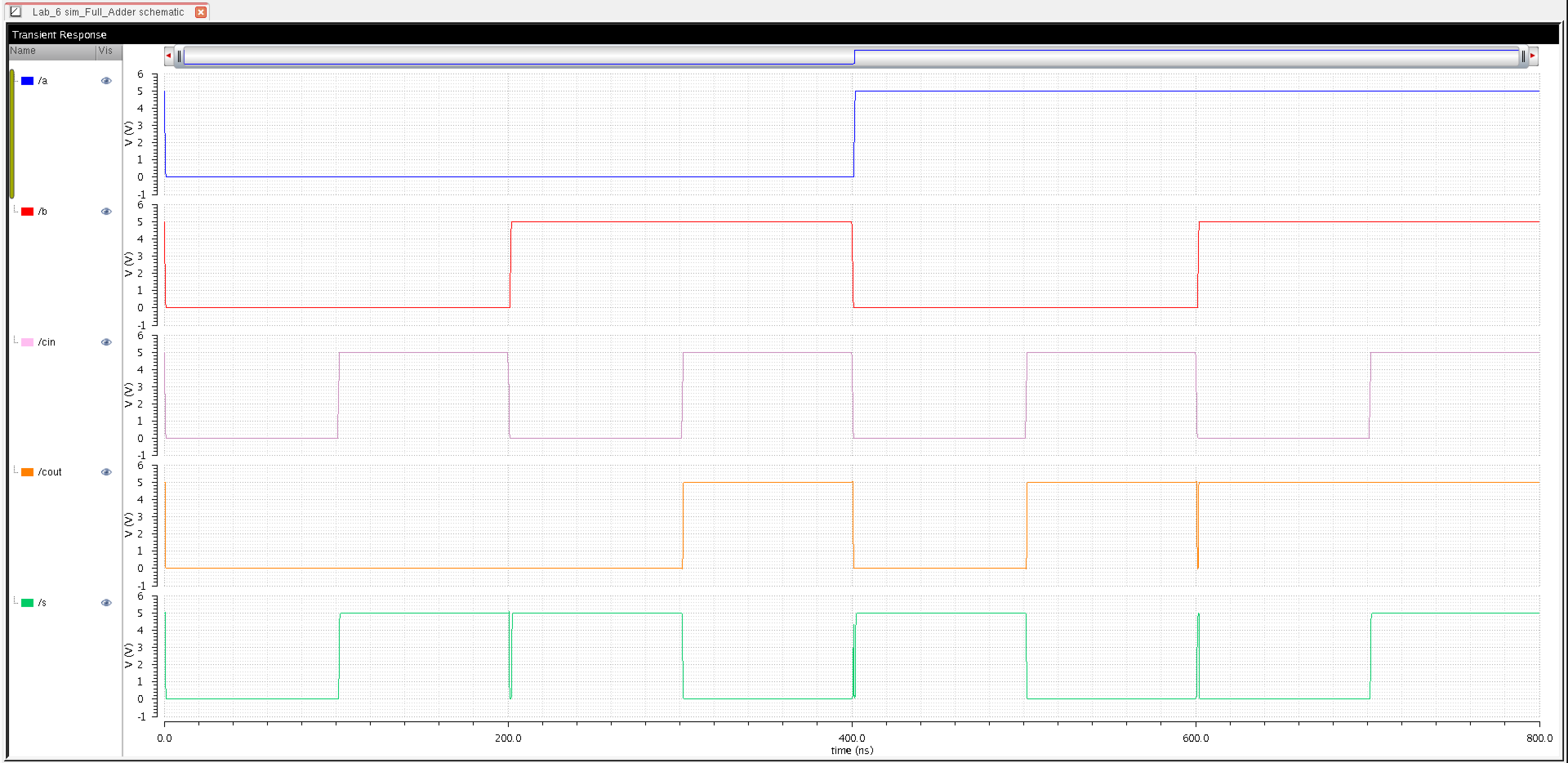 Fig 22
Again we see
that our simulation matches the expected results. We again notice glitches in
the outputs at t = 200, 400 & 600ns for the s output and at t = 600ns for
the cout output.
Back up all
files
 |