Lab 5 - ECE 421L
Design, layout, and
simulation of a CMOS inverter
Prepared by:
PRELAB WORK:
Back-up all your work from the lab and the
course
|
|

LAB WORK:
Draft schematics, layouts, and symbols for two inverters having sizes of:
12u/6u
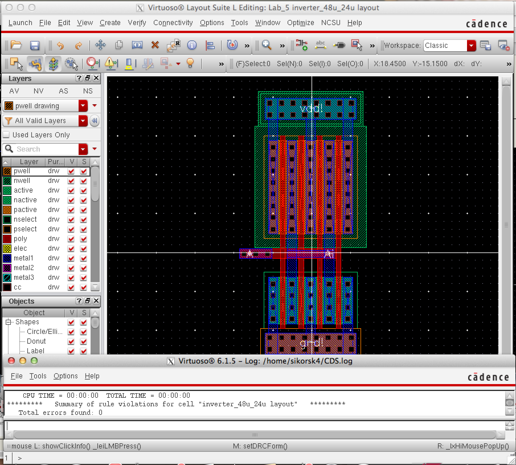
48u/24u where the devices use a multiplier, M = 4
We used Tutorial 3 to draft the schematic, symbol and layout view of the 2 inverters
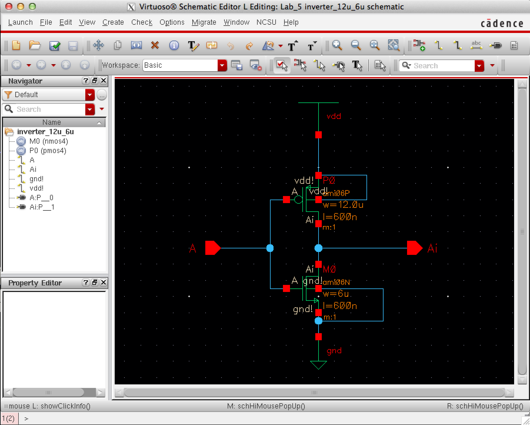
Schematics:
The schematics were created using NMOS4 and PMOS4 from the design library.
|
|
|

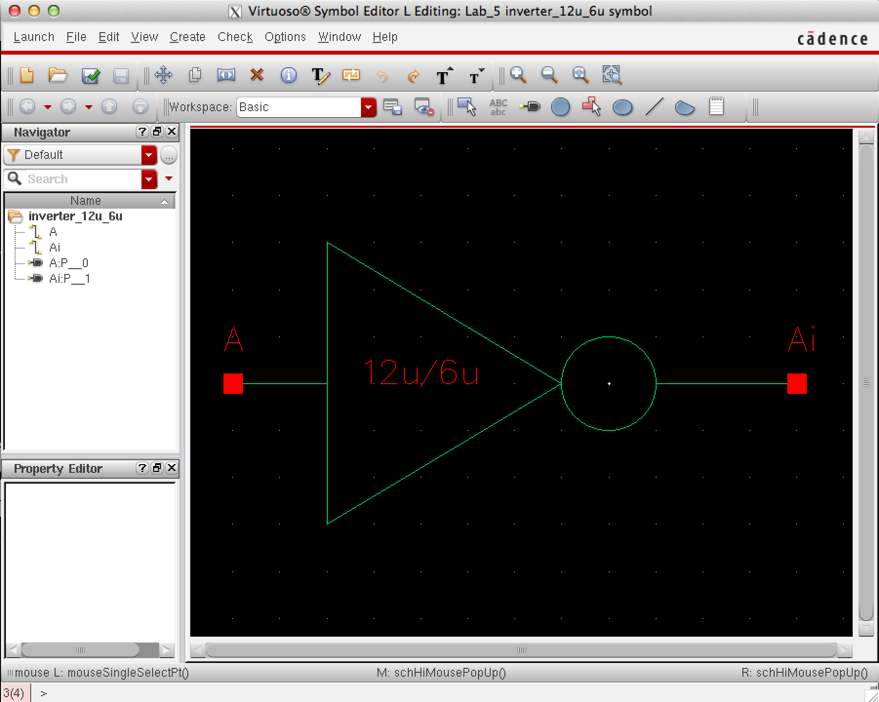
Symbols:
The symbols were created from the schematic by creating cell view from cell view.
|
|
|

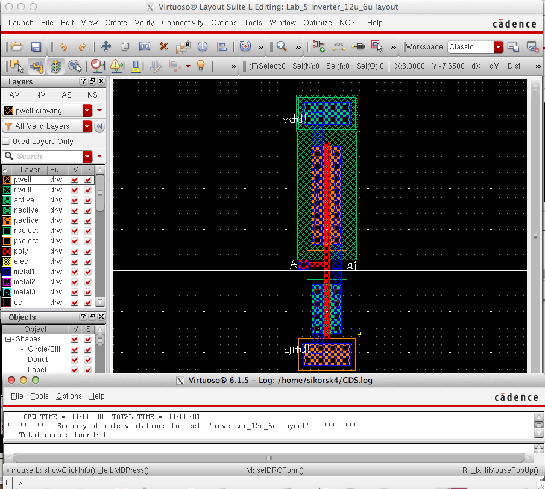
Layouts:
The layouts were verified and a DRC was ran to ensure no design rules were violated.
|
|
|
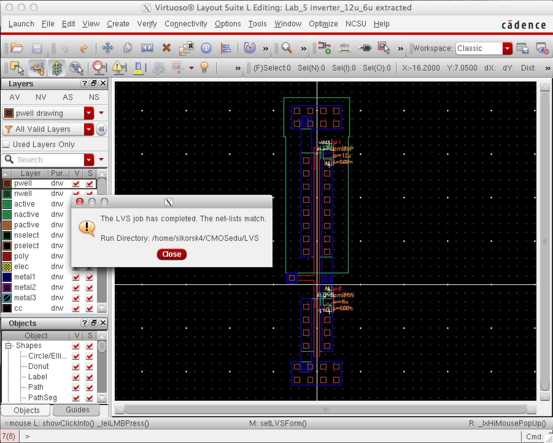
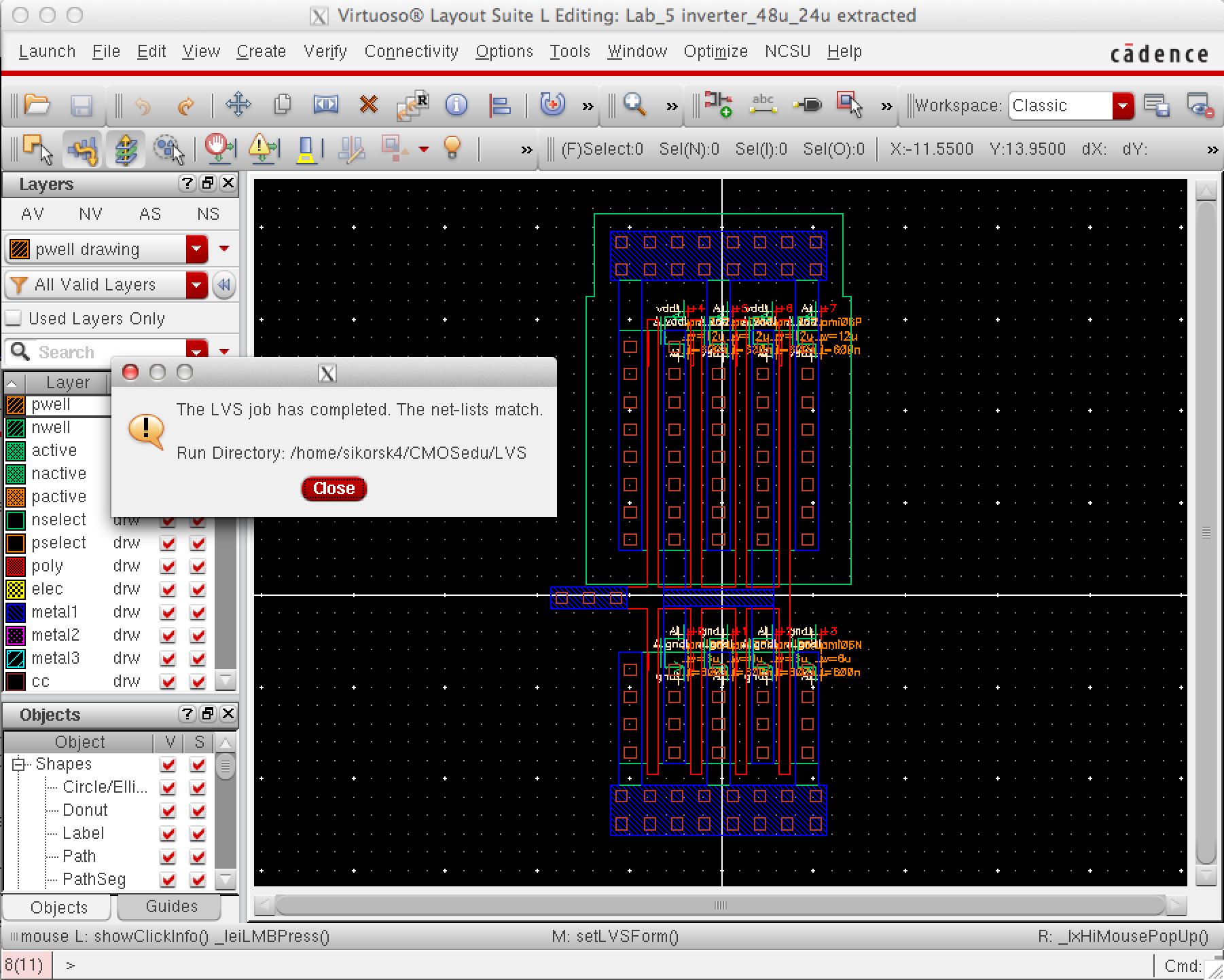
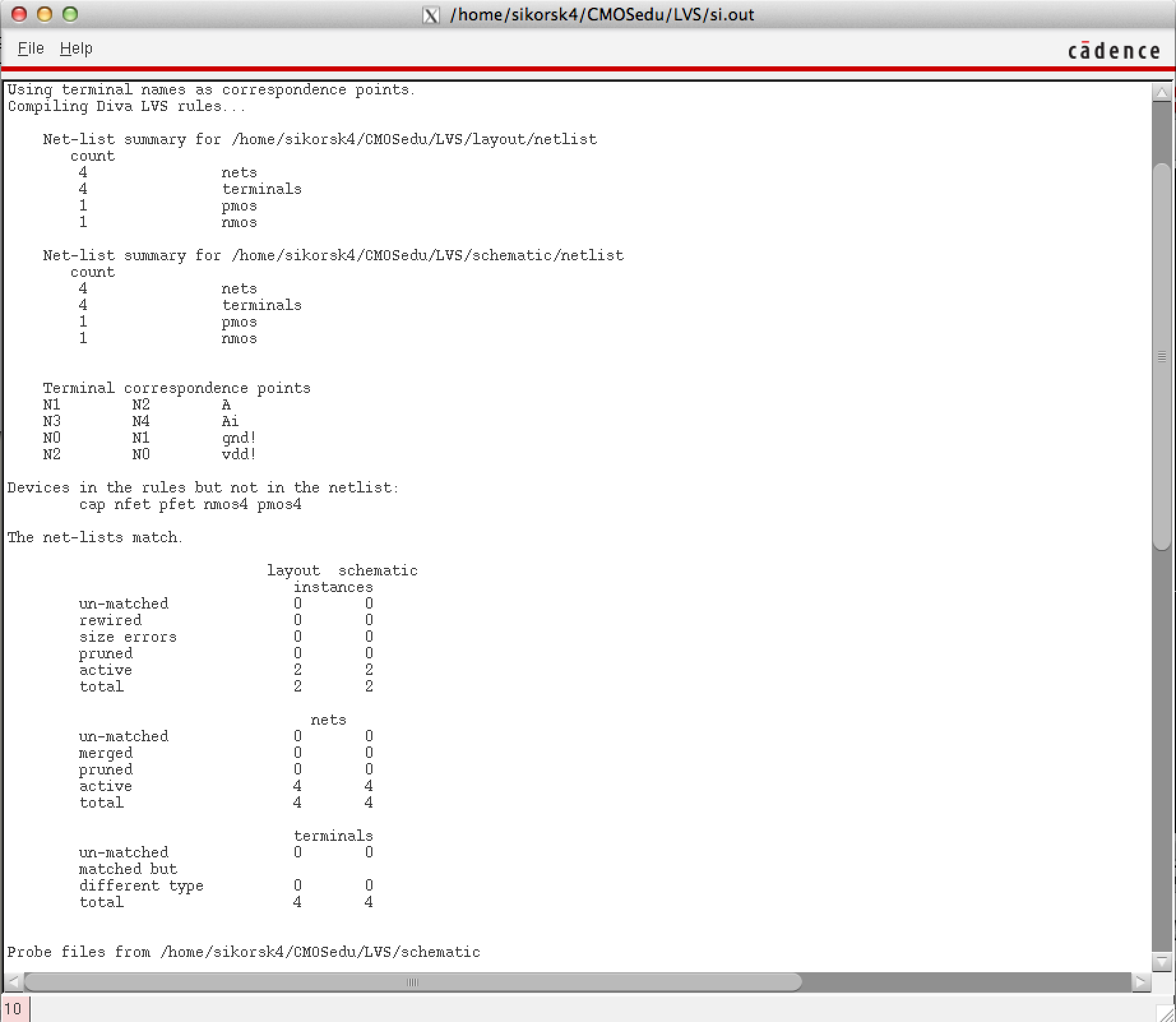
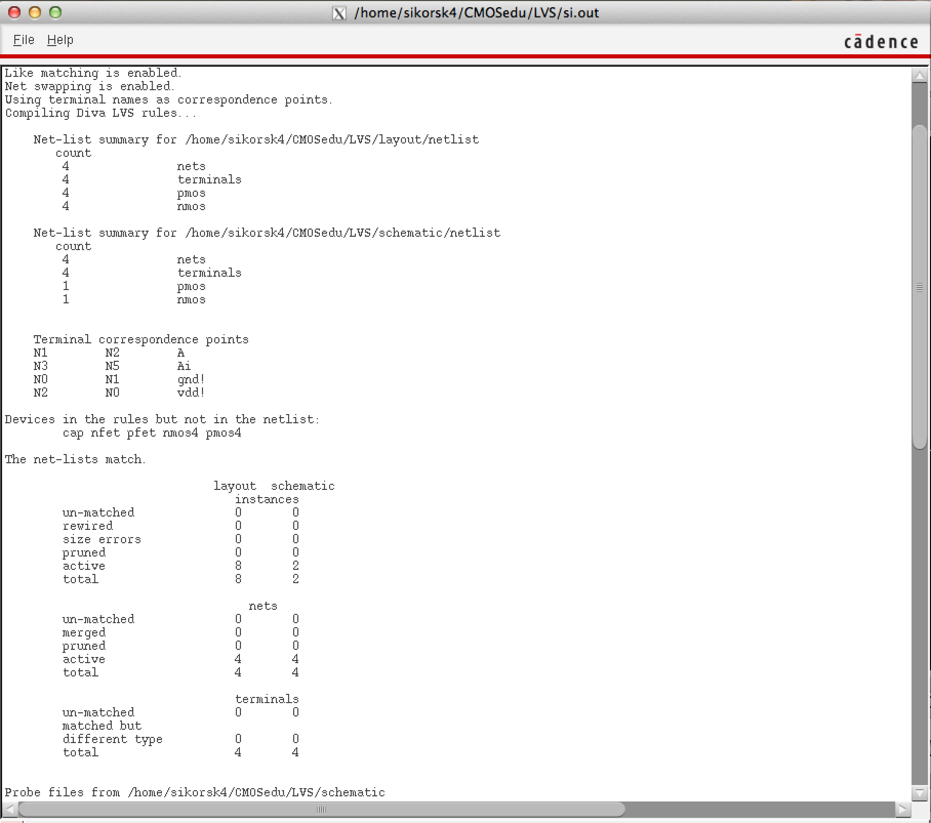
Extracted View:
The layouts were extracted and an LVS was run
using the schematics previously created.
|
|
|
Using SPICE
simulate the operation of both of your inverters showing each driving a 100 fF, 1 pF, 10 pF, and 100 pF capacitive load
Comment, in your report, on the
results
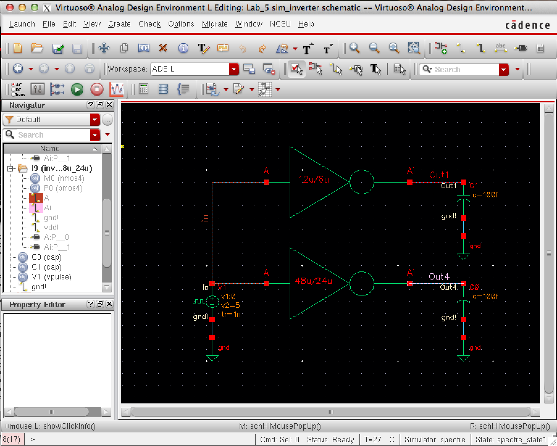
Schematic:
We created a schematic to simulate the operation
of both inverters.
|
|
|
Simulation with 100fF
|
| Simulation with 1 pF
|
|
Simulation with 10 pF
|
|
Simulation with 100 pF
|
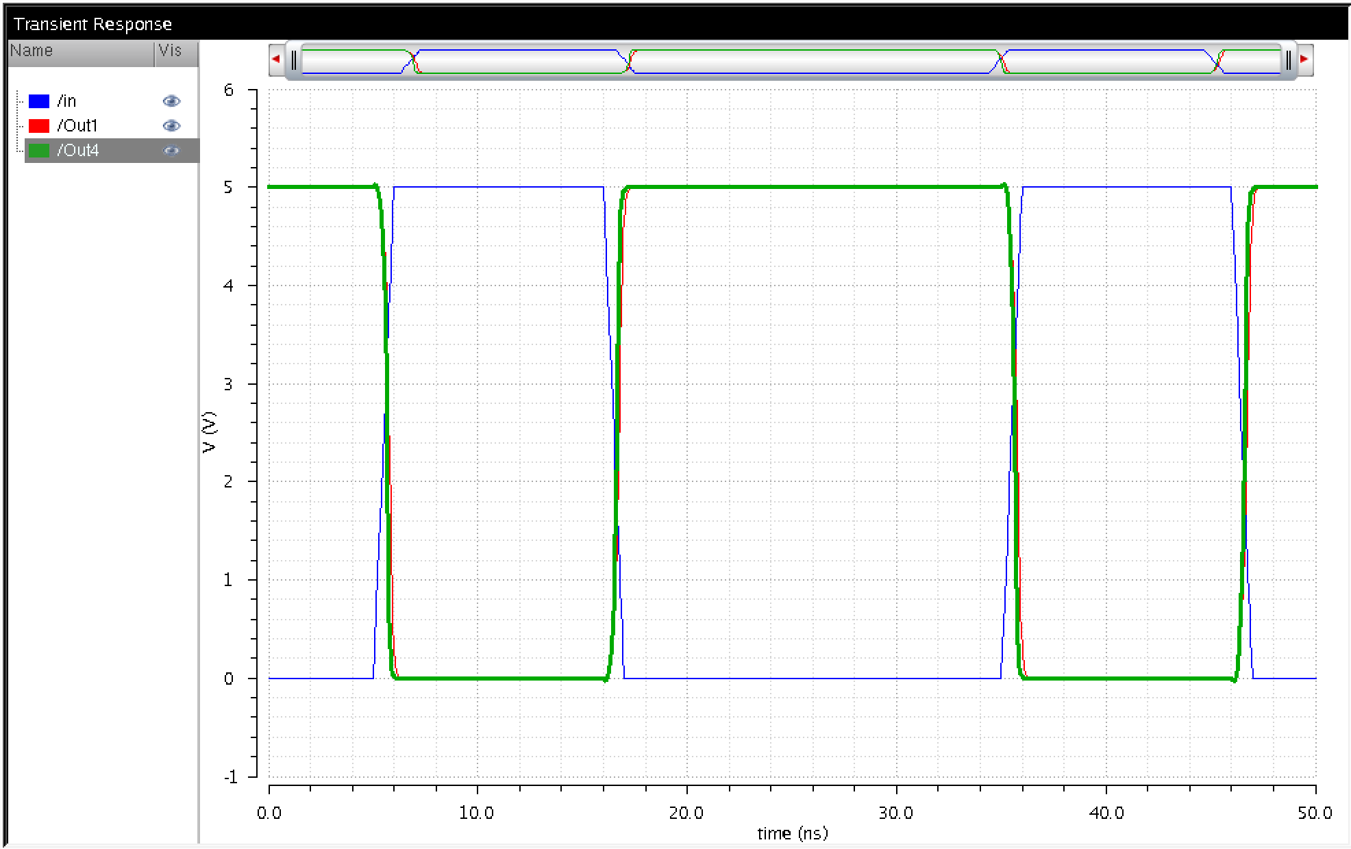
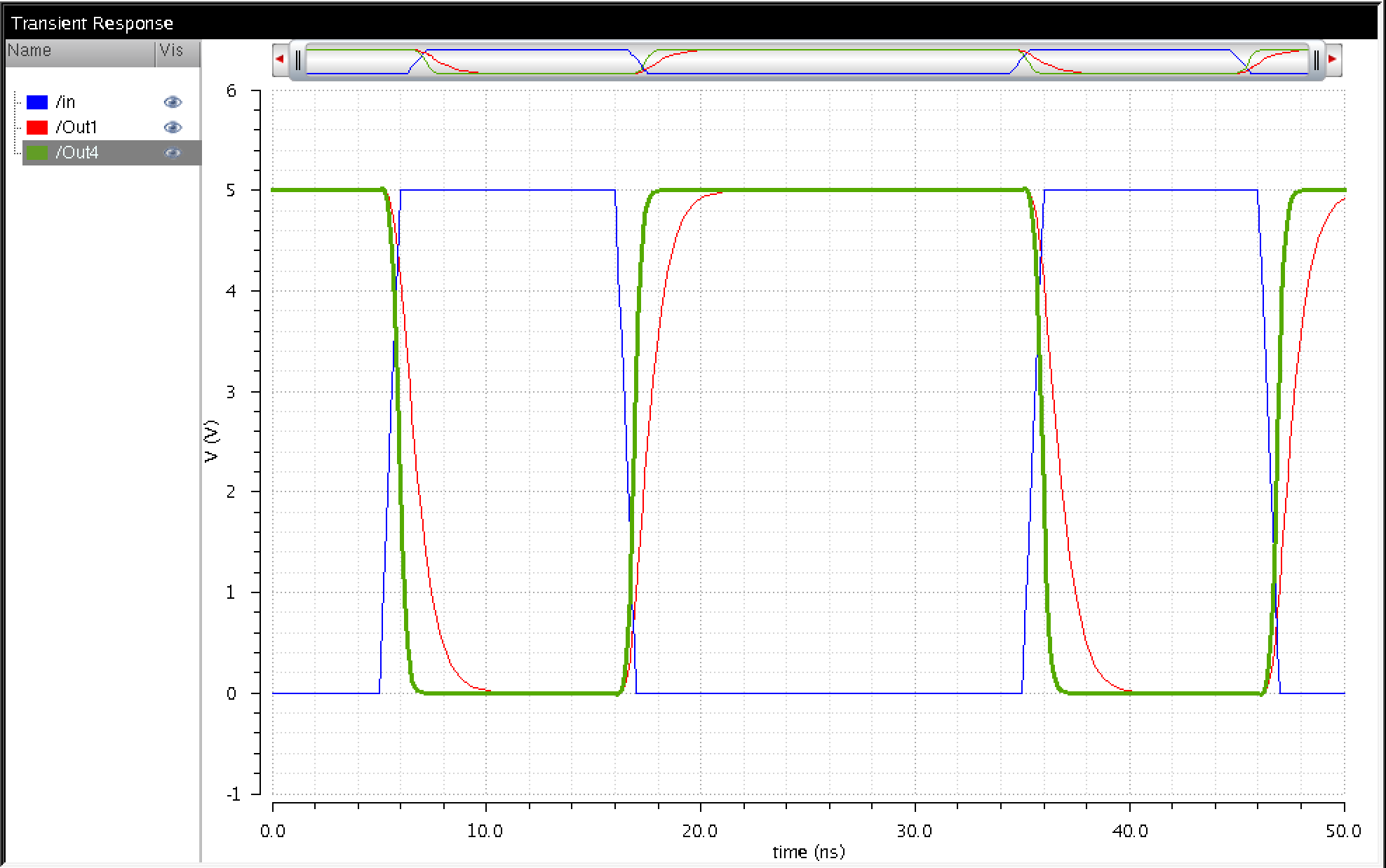
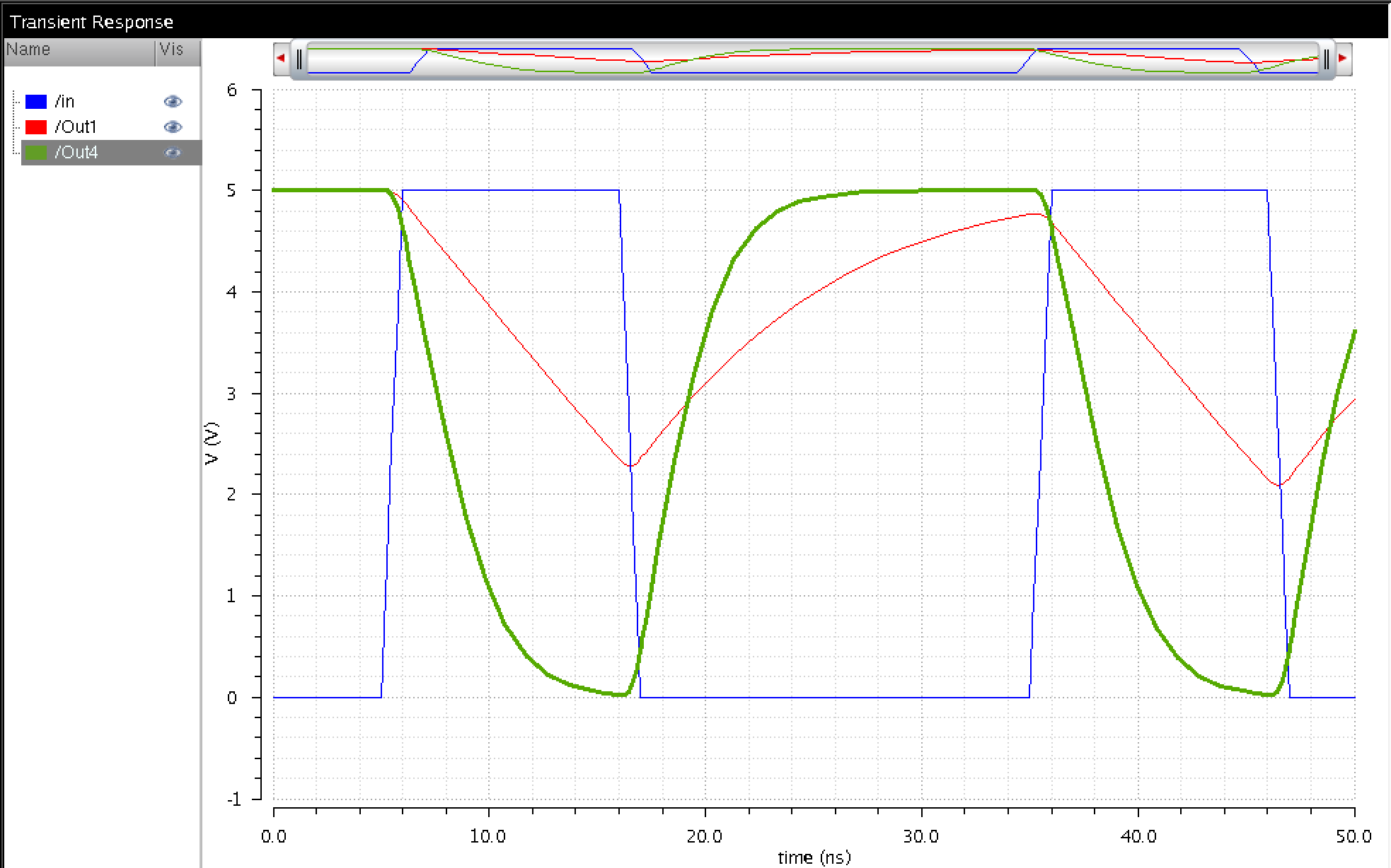
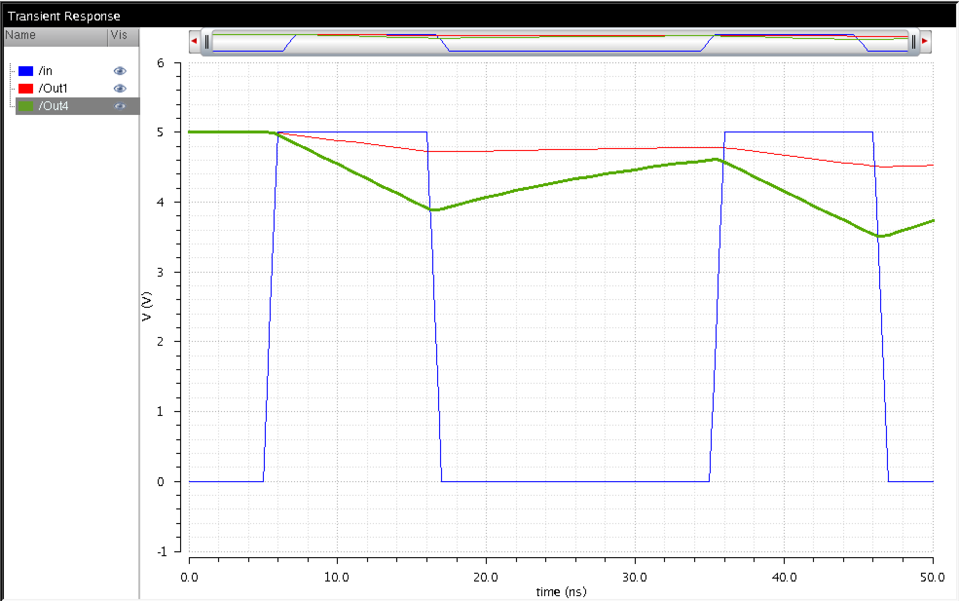
We noticed that the larger the inverter the smaller the rise and fall time are because more current is able to flow from the drain to the source.
Back up all files
|
|
