Lab 3 - ECE 421L
Layout of a 10-bit digital-to-analog converter (DAC)
Prepared by:
Jason Sikorski
PRELAB WORK:
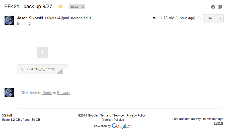
All files
for EE421L were zipped, backed up and emailed.
|
Fig 1 |
Tutorial 1
had been finished previously as a part of Homework #4 A2.6
LAB WORK:
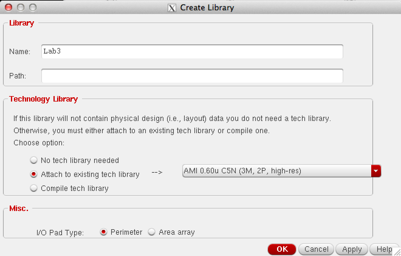
A new
library for Lab 3 was created, ensuring to attach the correct tech library for
the C5N process.
|
Fig 2 |
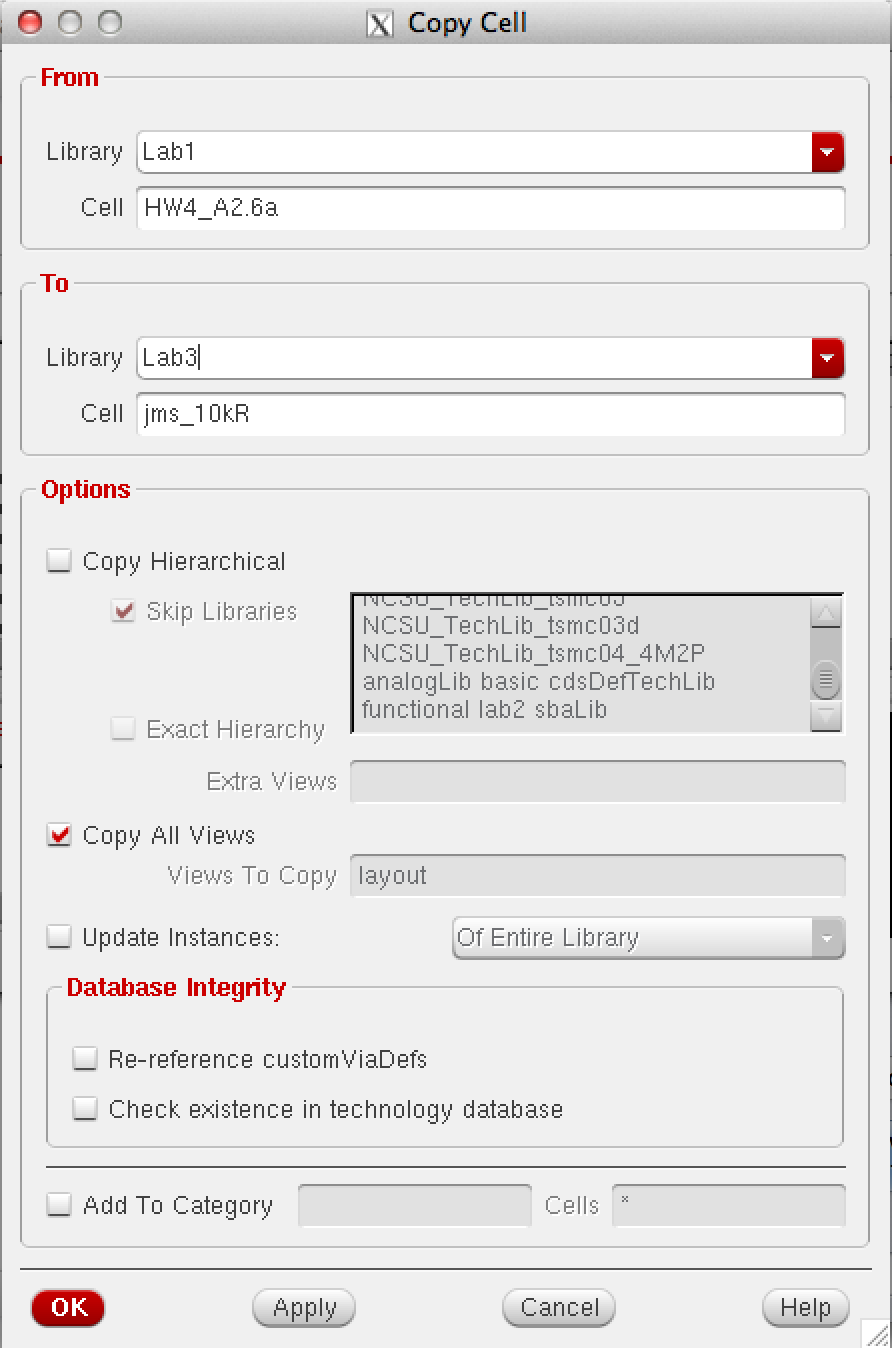
The layout from
Tutorial 1 and HW #4 was copied to the Lab 3 library.
|
Fig 3 |
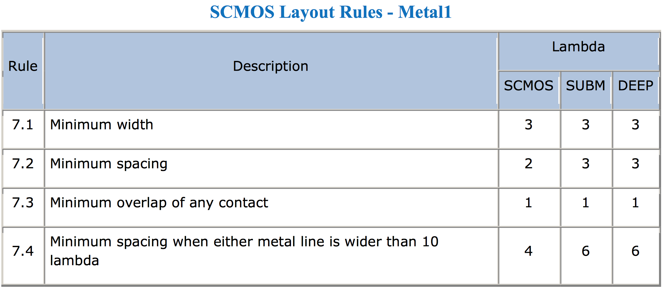
The design of
a resistor with a 10kΩ resistance in an n-well with a sheet resistance of
800Ω requires 10k/800 = 12.5 squares. Using the MOSIS scalable CMOS
design rules, with a λ of .3µm, a min well width of 12λ and well
spacing of 18λ , a 12λ*0.3µm = 3.6µm width is required and a 12.5*3.6µm
= 45µm length is required.
|
|
|
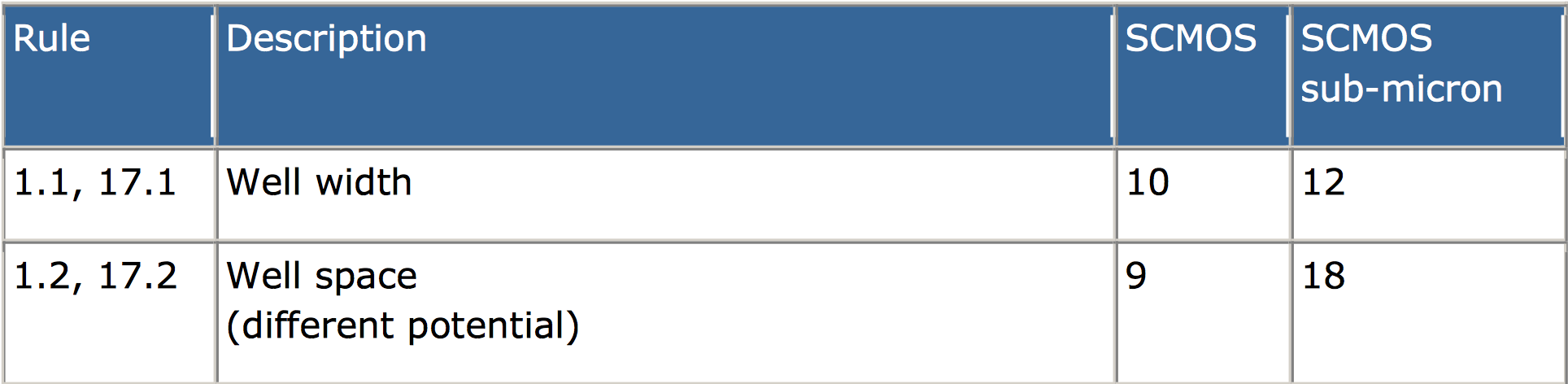 Fig 4.1
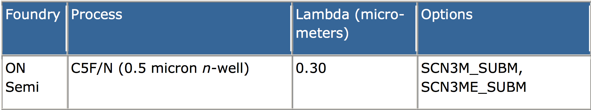 Fig 4.2
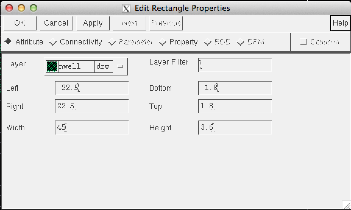
The
dimensions for the n-well resistor from HW#4 were edited to the calculated
requirements.
|
Fig 5 |
A Design
Rule Check (DRC) of this layout was performed and zero errors were found.
|
|
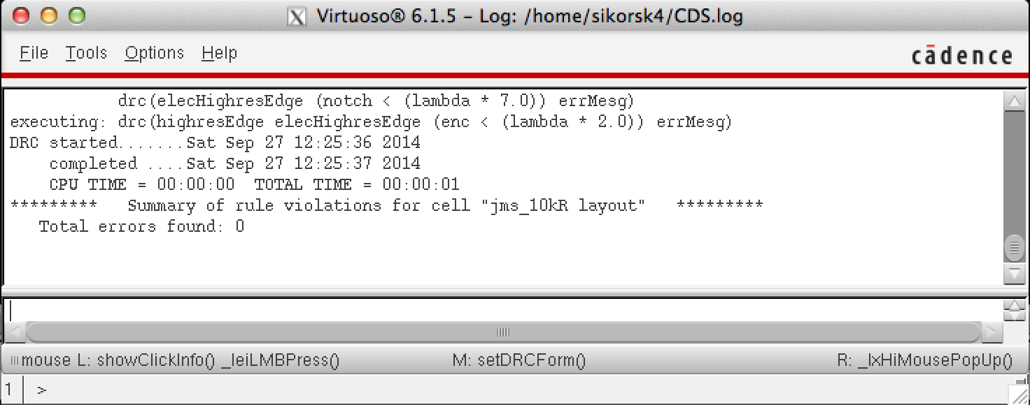 Fig 6
Fig 6The layout
was extracted and a resistance of 10.24kΩ was observed. This is a percent
error of 2.4% which is acceptable for this application. This deviation in
resistance will not have any effect on our voltage divider as the same layout
is being used for each resistor. This will allow us to generate the expected 1
to 2 divider.
|
|
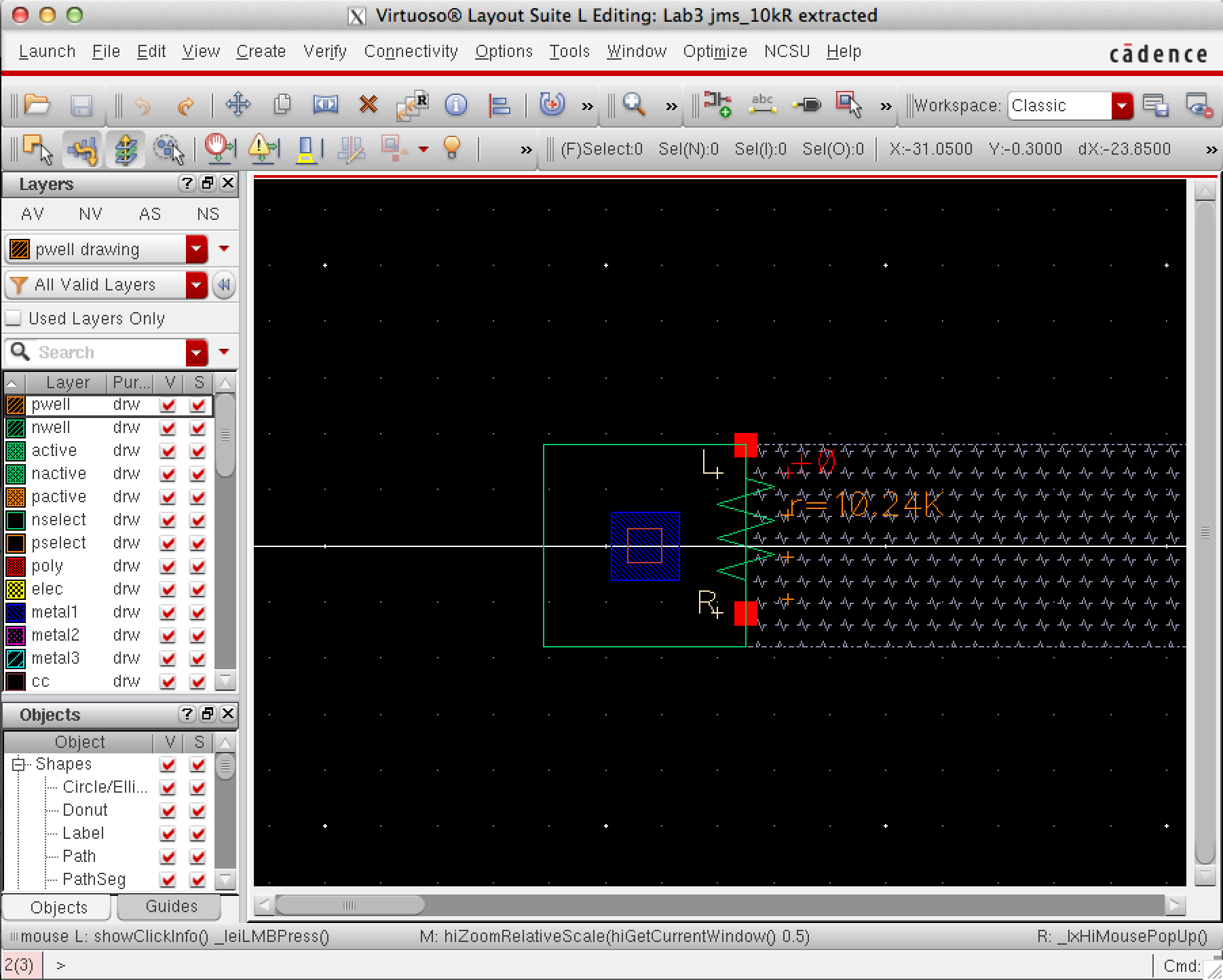 Fig 7
Fig 7A new layout
cellview was created for our R2R layout. In this
layout we instantiated our resistor layout. From the MOSIS SCMOS we know that
these n-well resistors must be have a minimum spacing of 18λ, for this
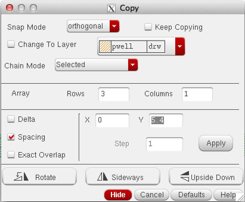
design that equals 0.3µm * 18 = 5.4µm. The instantiated resistor was copied to
a 3x1 array with Y spacing of 5.4 to ensure all spacing requirements were met.
|
Fig 8 |
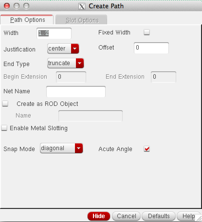
To connect
the 3 resistors, a metal 1 layer was used. A width of 4λ or 1.2µm was used, this is
wider than the MOSIS SCMOS requirements of minimum width of 3λ.
|
Fig 9 |
|
Fig 10 |
In, Out and GndOut pins were placed on the layout to match the pins
from our R2R schematic from lab 2.
|
|
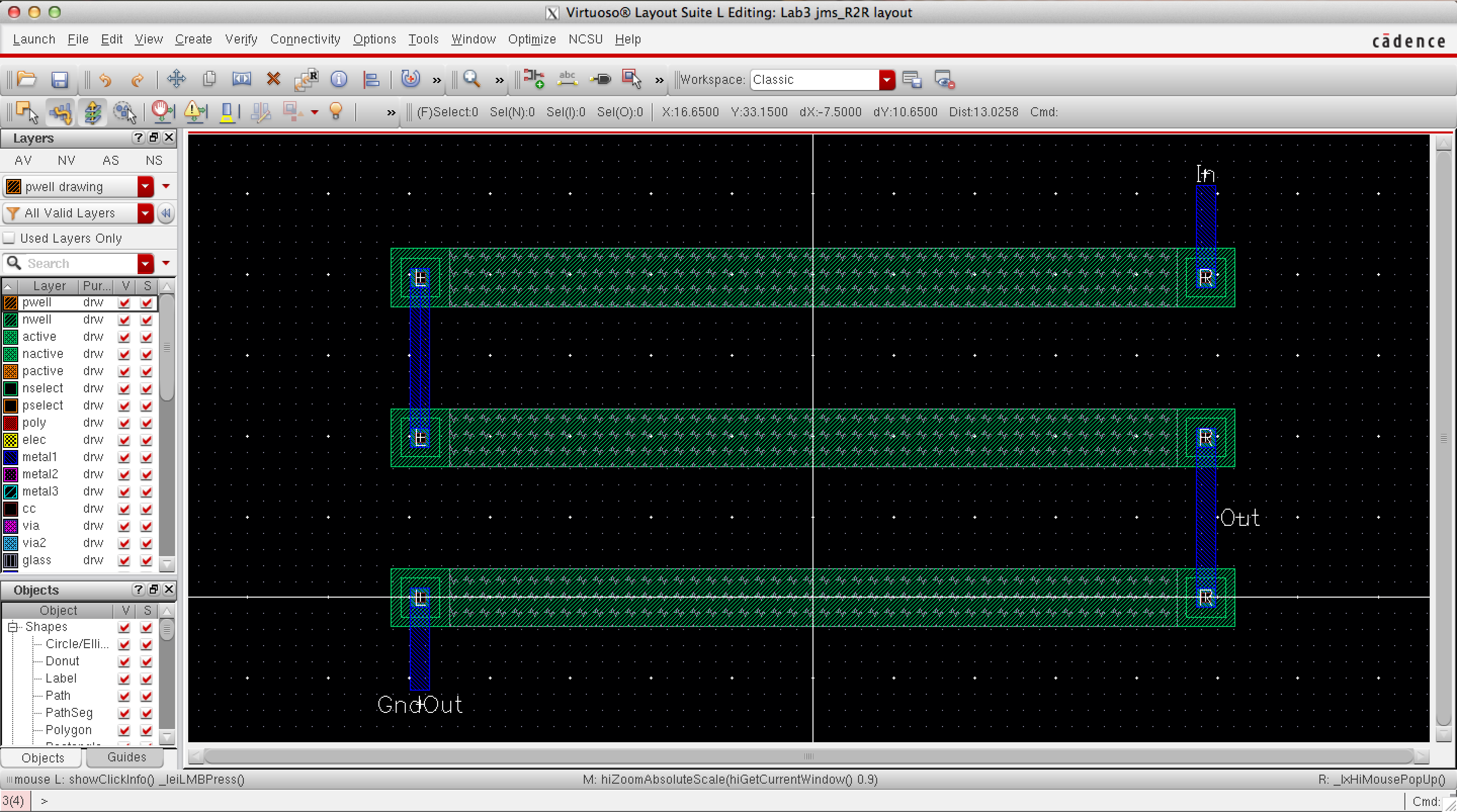 Fig 11
A DRC of the
layout was performed and zero errors were found. The layout was then extracted.
|
Fig 12 |
|
|
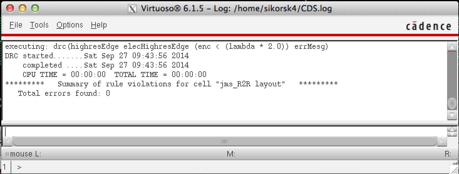
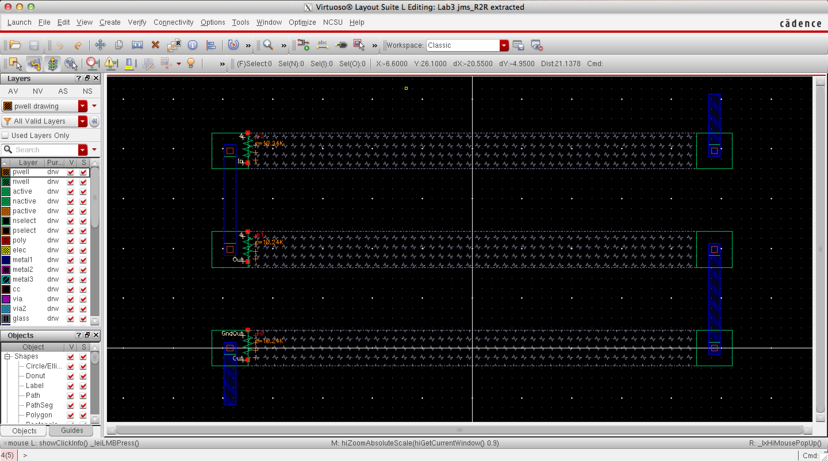 Fig 13
A Layout
Versus Schematic check was performed to compare this layout with the R2R
schematic from lab 2 and zero errors were found.
|
Fig 14 |
|
Fig 15 |
|
|
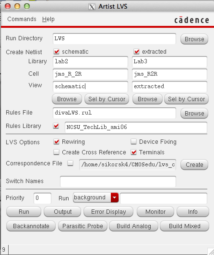

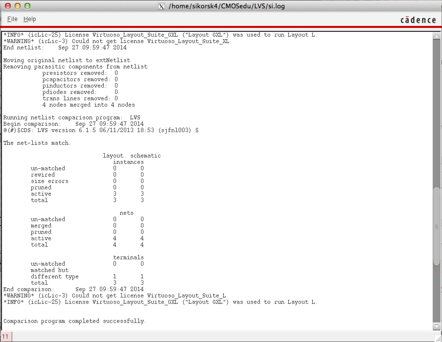 Fig 16
All files were zipped and emailed for backup