Lab 2 - ECE 421L
Design
of a 10-bit digital-to-analog converter (DAC)
PRELAB WORK:
The
lab2.zip file was downloaded and upload to the CMOSedu design directory. This
directory was then defined in the cds.lib in the design directory to ensure the
examples would show in Cadence.
|
Fig 1 |
|
 Fig 2
Fig 2The
sim_Ideal_ADC_DAC schematic was opened and the
simulation run. The simulation plot background color was changed to white, line
thickness changed to medium, style changed to solid and color changed to red
and blue.
|
|
|
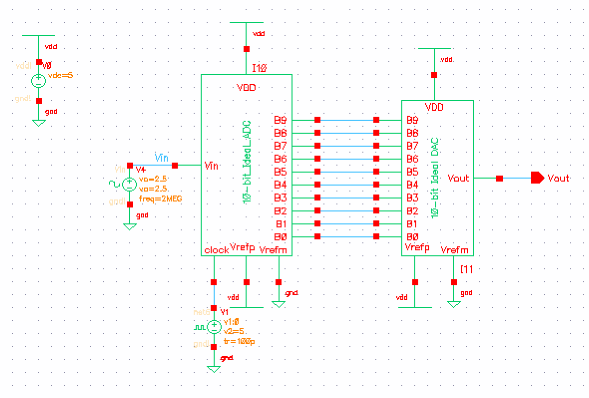 Fig 3
Fig 3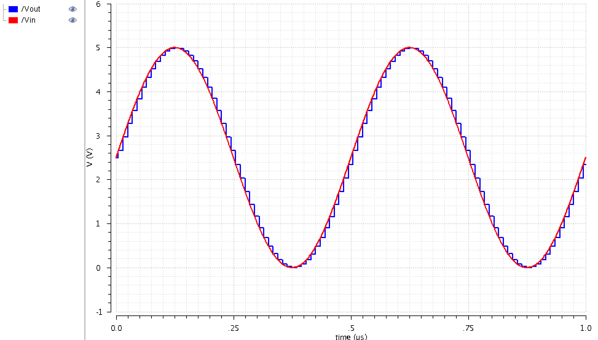 Fig 4
Fig 4LAB WORK:
This lab
required us to design our own 10 bit DAC using a 2 to 1 resistor voltage
divider. A schematic named R2R was created and a voltage divider was designed
with in, out and gnd out pins. A symbol for this
schematic was then created for hierarchy implementation into our 10 bit DAC.
|
|
|
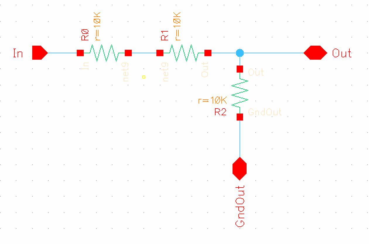 Fig 5
Fig 5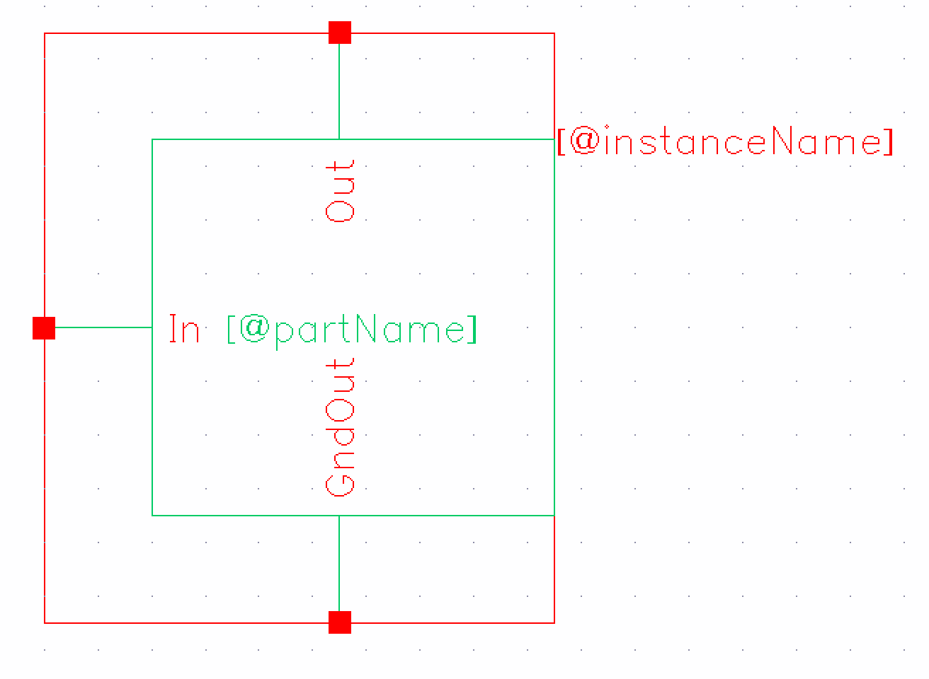 Fig 6
Fig 6Since the
file ideal_10-bit_DAC already had the design layout we needed, this file was
copied and the old ideal_DACbit's were replaced with
the new R2R voltage dividers we designed in the previous step. This file was
saved and a new symbol was created.
|
|
|
|
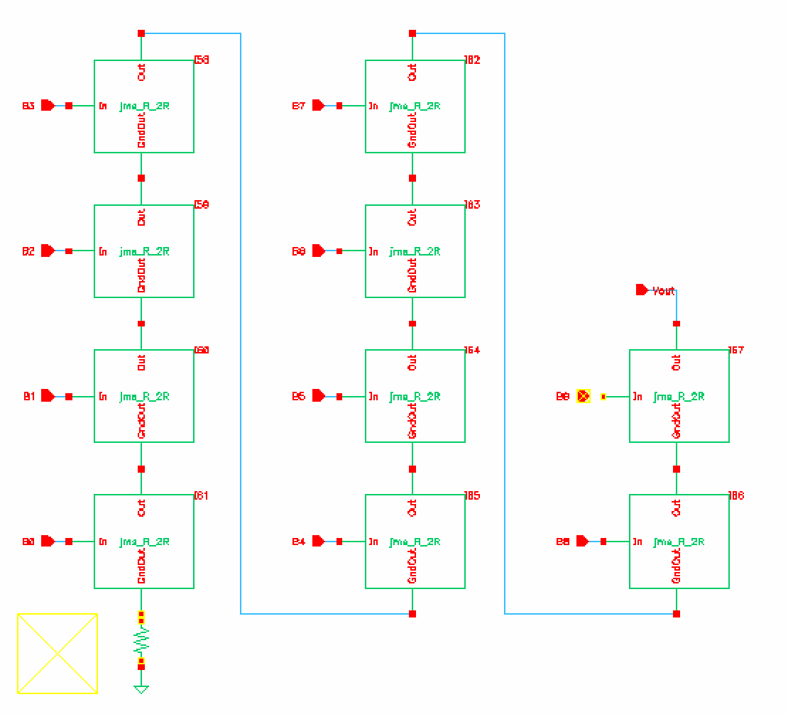 Fig 7
Fig 7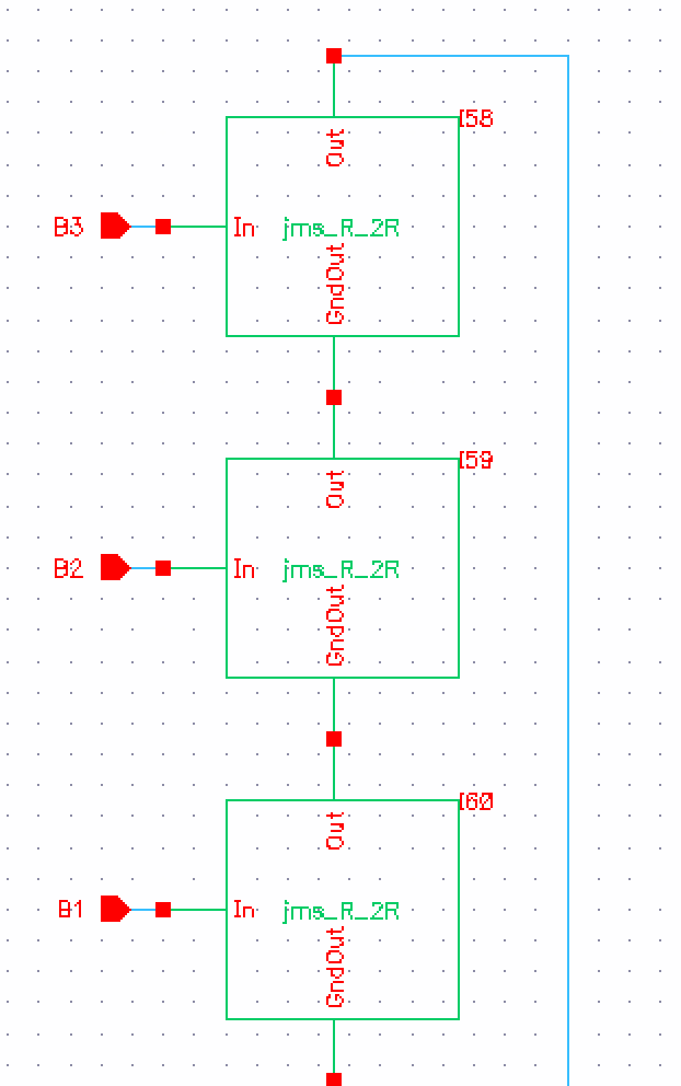 Fig 8
Fig 8 Fig 9
Fig 9To ensure
our 10 bit DAC was designed properly we replaced the original 10-bit_ideal_DAC
in the simulation file with our 10 bit DAC and renamed the file. We then launched
the Analog Design Environment and ran a transient simulation for 1 us plotting Vin and Vout. The results
received matched the results that were seen in the prelab,
verifying our design.
|
Fig 10 |
|
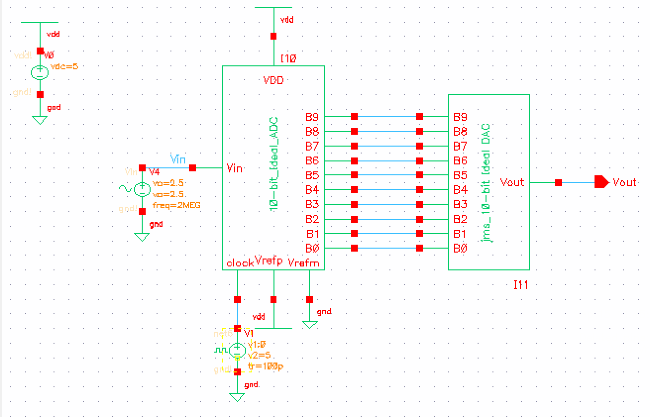
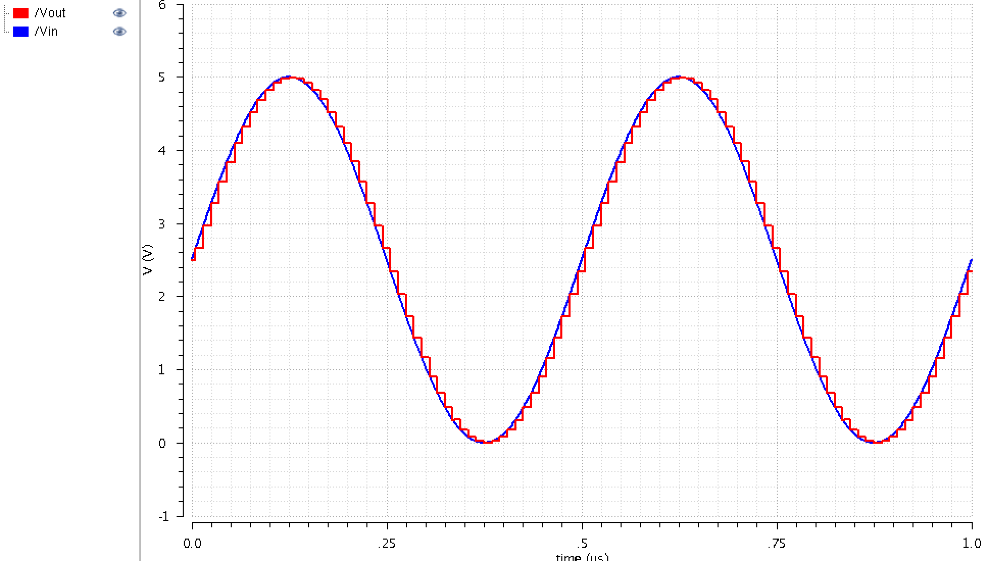 Fig 11
To calculate
the output resistance of the DAC we grounded the inputs from B0 to B9.
From this we can see that the 2R at the gnd of B0
is in parallel with the 2R from the input of B0. This results in an
output resistance of R. This resistance is in series with B0's
output resistance of R for an output resistance of 2R, which is then the input
resistance to B1. This cascades through the DAC and creates an Req of 10k Ohms.
|
|
|
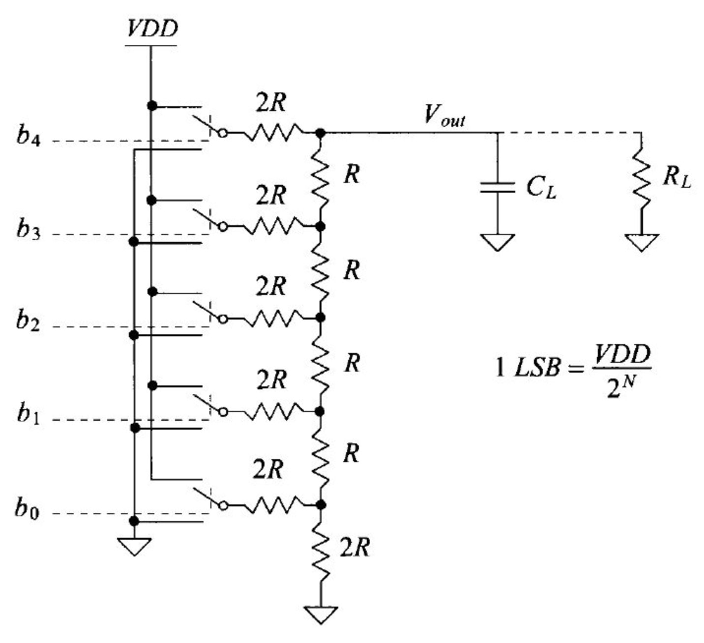 Fig 12
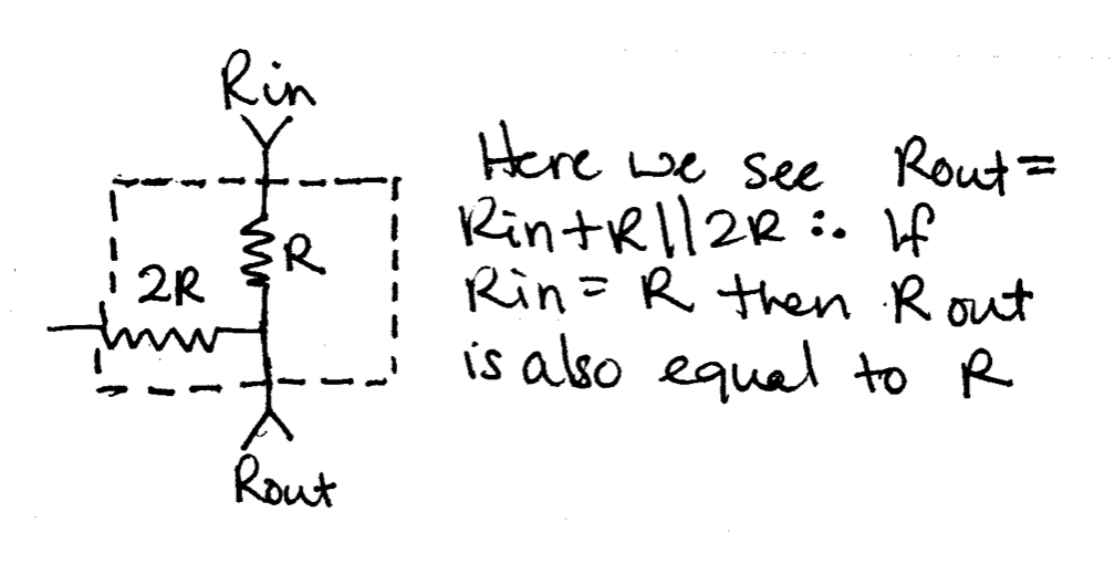 Fig 13
We then
calculated the delay driving a load. To do this inputs B0 to B8
were connected to gnd while B9 was
connected to a 5V pulse signal and the output connected to a 10pF capacitor. We
can calculate the expected results to be equal to 0.7RC, or in this case 70ns
with an output equal to 1/2 vin. This was confirmed
by our Cadence simulations.
|
|
|
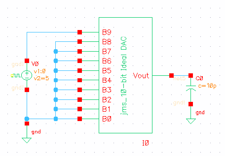 Fig 14
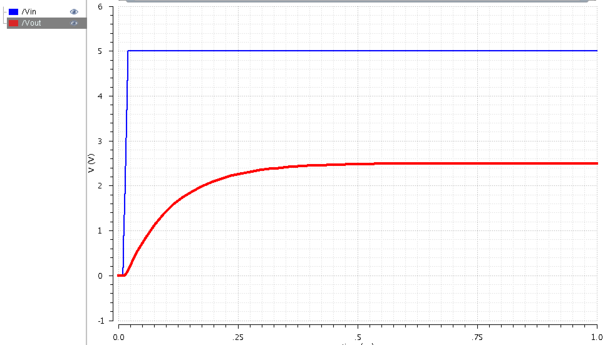 Fig 15
For
calculating the DAC driving a load we can simply replace the DAC with a 10k
resistor and hand calculate the output. To show this we simulated the DAC
driving a 10k resistor, a 10pF capacitor and a 10k resistor in parallel with a
10pF capacitor.
|
|
|
|
|
|
|
|
|
|
|
Fig 24 |
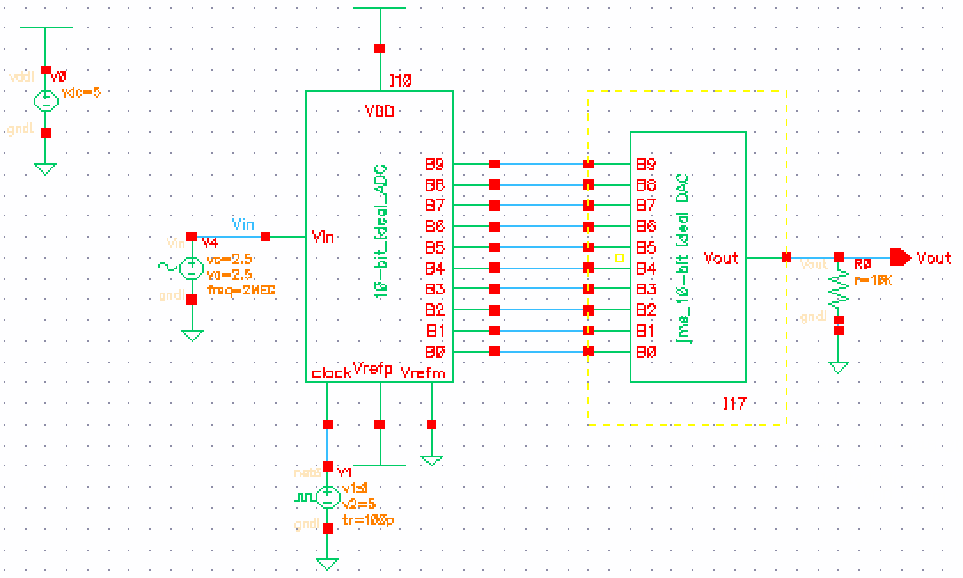 Fig 16
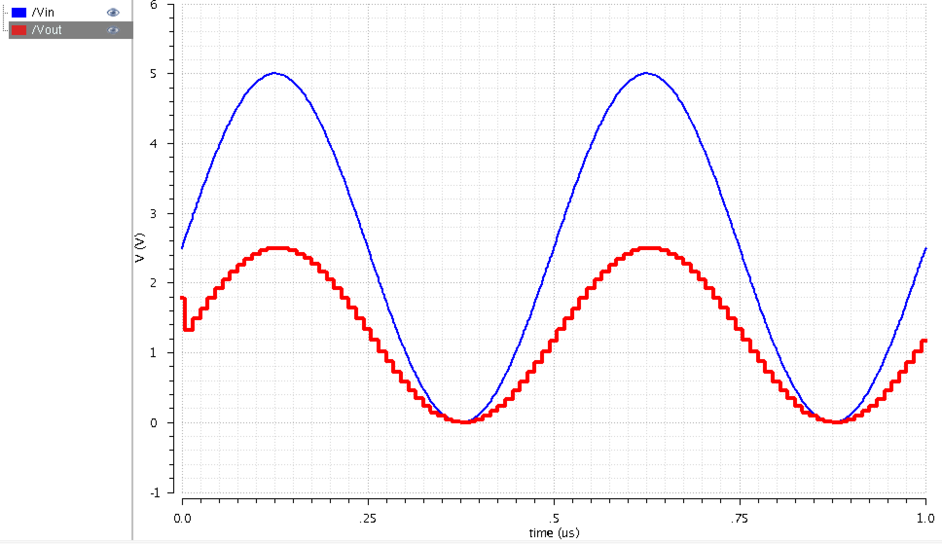 Fig 17
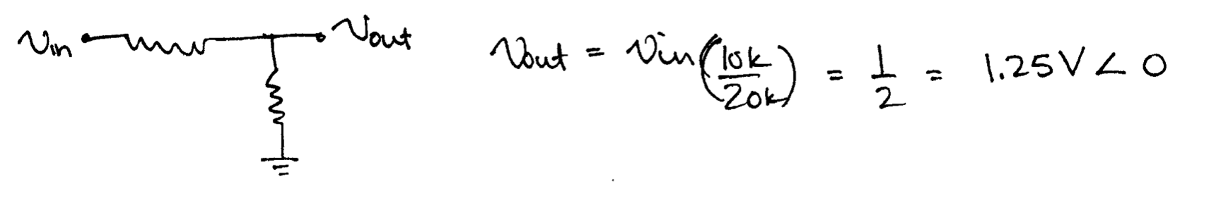 Fig 18
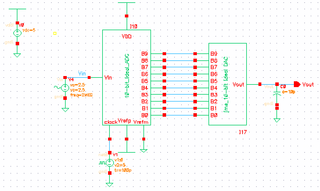 Fig 19
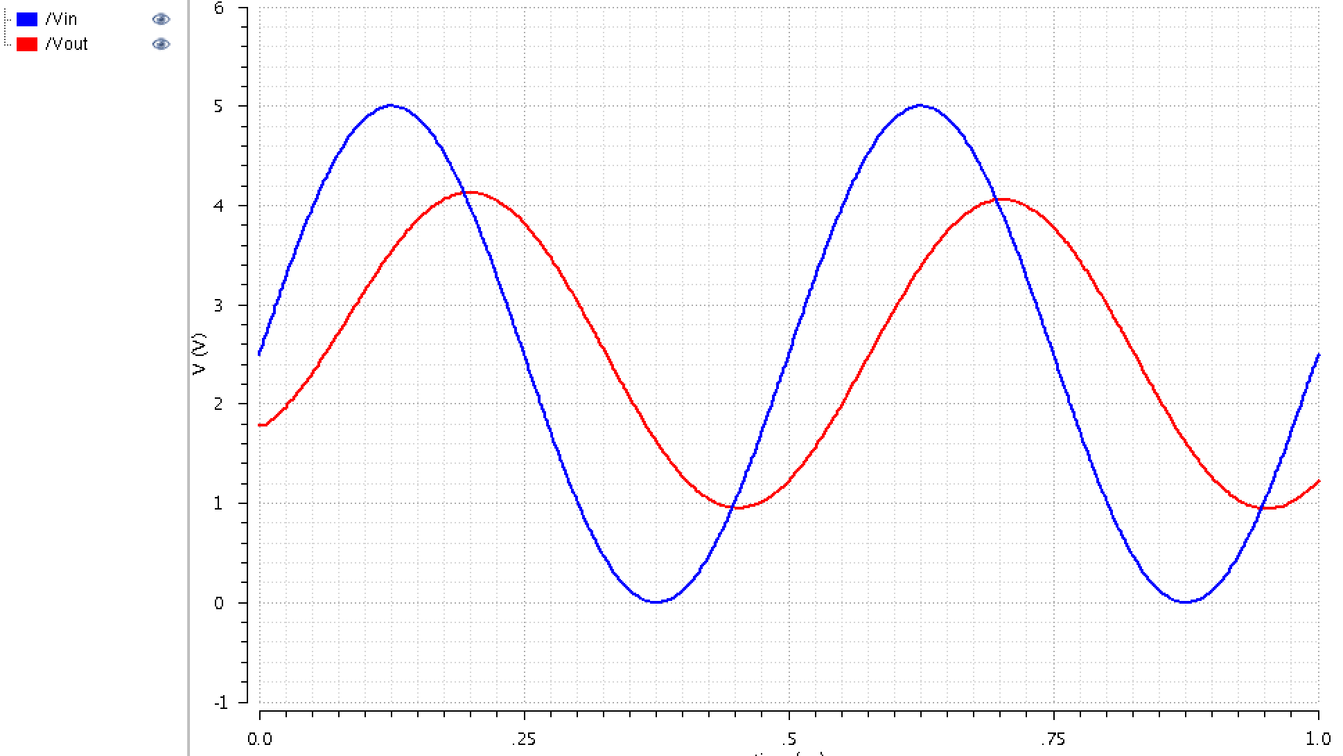 Fig 20
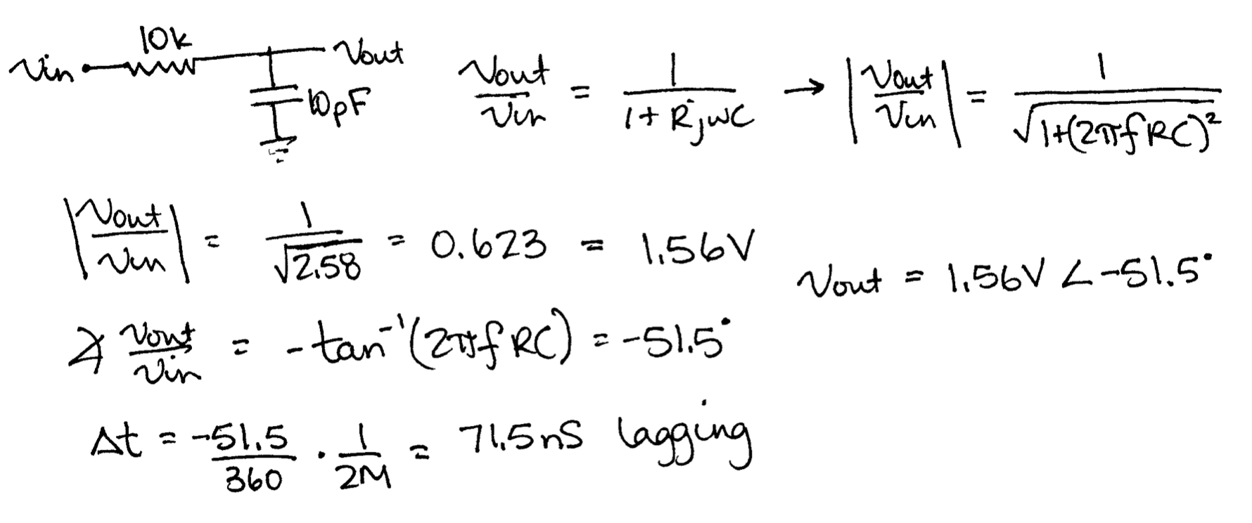 Fig 21
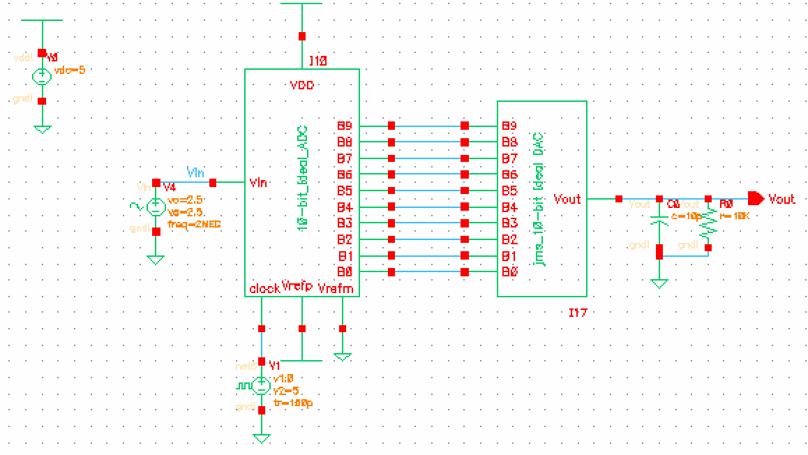 Fig 22
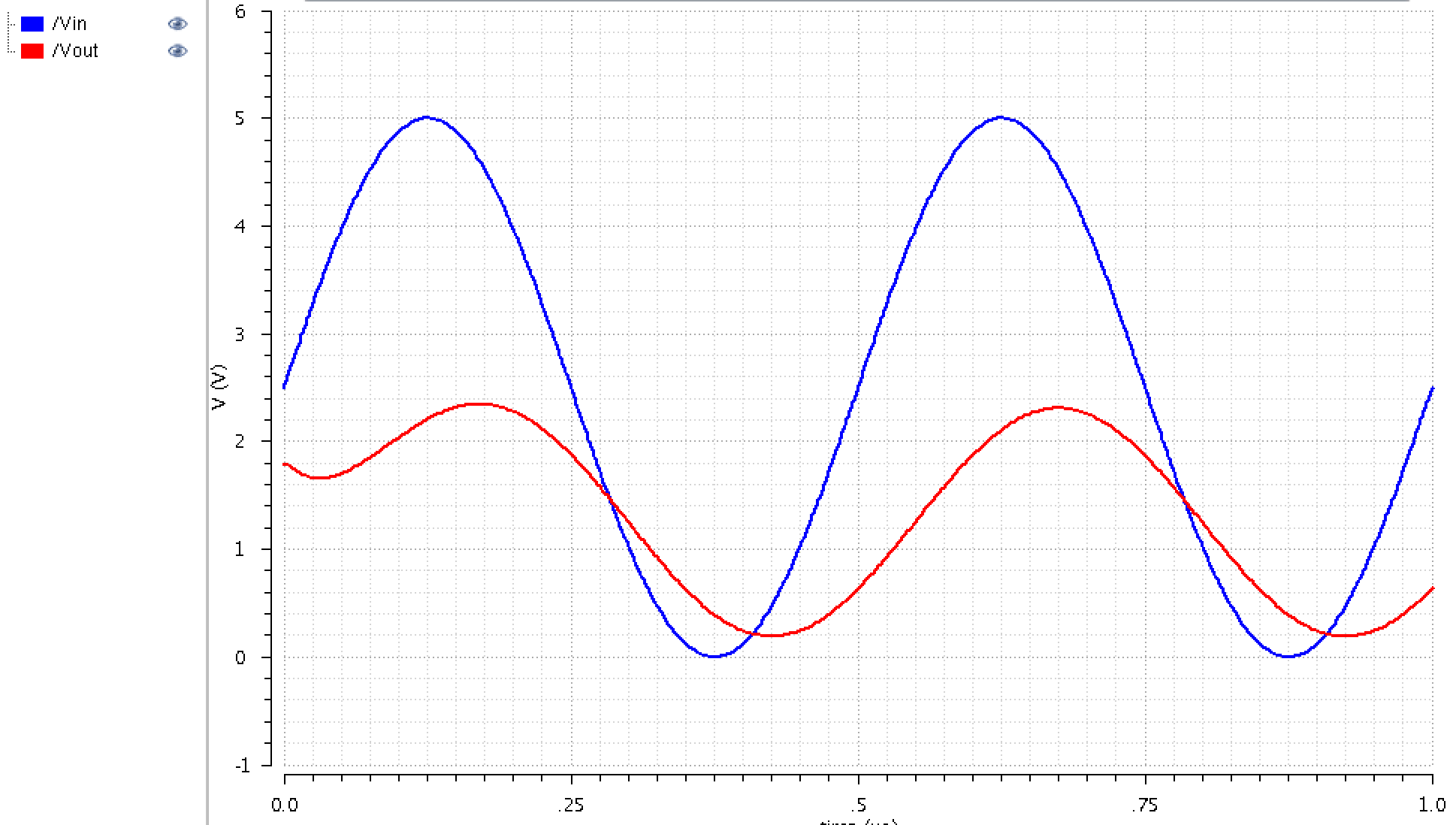 Fig 23
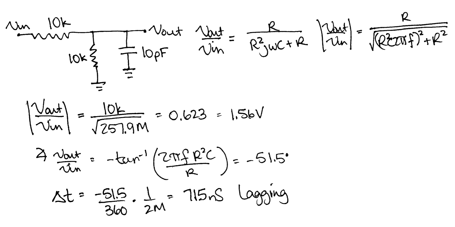
If the resistance of the switches connected to the DAC was not significantly less than our value of R we would see a decreasing magnitude for our output voltage. As an example, let's use a 5k resistance for our input switches. Instead of having 2R in parallel with 2R, we would have 2.5R in parallel with 2R. Instead of getting an output resistance of 2R, we would get a resistance of 2.11R. so for the next input we would have 2.5R in parallel with 2.11R resulting in an output resistance of 2.14R and so on, with the output resistance ultimately growing to 2.5R.
This lab was zipped and backed up once completed.