Lab
X - ECE 421L
Authored
by Hongzhong Li,
Today's
date 10/18/2014
Design, layout, and simulation of a CMOS NAND gate, XOR gate, and Full-Adder
Lab
description
In
this lab we will draft the schematics and layout of a 2 input NAND
and a 2 input XOR gaates and then create a full adder using them.
Pre - Lab Work
Using MobaXTerm log into csimcluster.ee.unlv.edu. First we back up all our work from lab6 folder by downloading the file from the CMOSedu directory. Then email the file to our own email.

Drafting schematics, layouts, and symbols for the 2 inputs NAND gate and 2 inputs XOR gate
Launch Virtuoso.
In the library manager copy the files in lab 5 to lab 6.
We will now create a layout for the 2 inputs NAND gate. We will be using the inverter used created in lab 5 and then add extra instances. Create a schematic as seen in below.

Then go to create->cellview->from cellview. Create the NAND symbol as seen below.

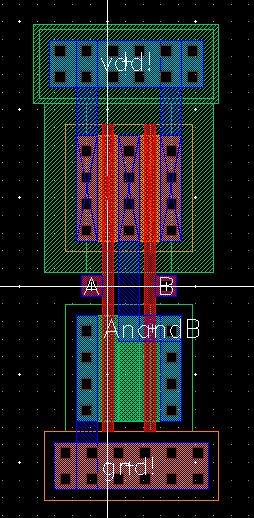
Layout for the 2 Inputs NAND gate
We need to avoid the AnandB pin from touching the metal1 of the nmos. Go to edit->hierarchy->flatten. Unselect preserve pins geometries. Select flatten pcells, and flatten vias. We can now delete the vias and metal 1 in the middle.
Change the pmos and width to 6u per lab requirements. Add the AnandB pin as ouput.
LVS Result for 2 Inputs NAND gate
Simulation result -2 Inputs Nand gate
Create a new cell view schematic for the simulation.


2 Inputs XOR gate Schematic

After creating the schematic, create the symbol.

Afterwards DRC and LVS.
LVS Result for 2 Inputs Xor gate

Simulation result -2 Inputs Xor gate
Similar to the NAND gate we did before, use ADE-L to do a transient analysis.
Drafting schematics, layouts, and symbols for the Full Adder
Now that we have the NAND and XOR gates, we can now start making the full adder (FA).
I
placed metal 1 to poly and metal 1 to metal 2 vias on top of one
another where metal 2 connects with poly.
DRC and LVS the layout.

Full Adder Symbol

Full Adder LVS Result


For the final
step of the FA we must simulate the FA with 3 pulse sources. I used
10nS, 20nS, and 40nS periods with a transient time of 90nS.

NAND and XOR Gates Simulation

You
should have a ADE-L plot similar to the one below.

The ouputs of the simulation have glitches, this is due to the delays of the gates performed in each log operation.
This concludes the lab work. I back up my work as shown below.

Return to EE 421L Labs