Lab 4 - ECE 421L
Authored
by Hongzhong Li,
Email: lih12@unlv.nevada.edu
Today's
date: 10/03/2014
IV characteristics and layout of NMOS and PMOS devices in ON's C5 process
Lab
description
In
this lab we will create layouts and schematics for PMOS and NMOS
transistors of different sizes. Also we will simulate our layouts and
schematics to obtain the IV characteristics.
We begin by completing the MOSFETS in the tutorial. From this point we will create MOSFETS to be simulated for the lab.
Pre-Lab work
Using MobaXTerm log onto csimcluster.ee.unlv.edu
First we back up all our work from Tutorial_2 folder by downloading the file from the CMOSedu directory. Then email the file to our own email.

Launch Virtuoso from the /CMOSedu directory.
Creating the NMOS transistor
1) From the library manager, create a new schematic cell called NMOS_IV_3. Press I, go to the NCSU_Analog_Parts library, change the width of the nmos
to 6u and create the schematic below.

2) Next, we create a symbol for the nmos. Go to Create -> Cell View -> From Cell View and create the symbol below.

Check and save the symbol.
Creating the layout for NMOS transistor
1) Since the 3-pins NMOS transistor we created cannot be use for LVS run we have to create a 4-pins NMOS transistor. From
the library manager ->File-> New -> Cell View ->(schematic)
called NMOS_IV. Instaniate the NMOS transistor named "nmos4" from the NCSU_Analog_Parts library, change the width of the nmos to 6u and create the schematic below. (Again, the bulk of the NMOS is connected to ground).

Check and save the schematic.
2) We are now ready to create a layout for the NMOS. Go to Library Manager, Create, File -> New -> Cell View, create a cell (layout).
Next instantiate an nmos device from the NCSU_Techlib_ami06 and change the width to 6u.

You should now see the following nmos layout. If not, press e and change the Display Level(Stop) to 10.

Then add a metal1-connection-to-poly cell (m1_poly) and a poly rectangle to connect the gate to m1_poly. Next instantiate a ptap cell (metal1 connection to p+) in the p-substrate (Remember this is will be the bulk of the nmos which should be connected to ground). We will now add the pins to our nmos. Go to Create->Pin. Create pins G, D, S and B as below.

Save and DRC to check for errors. Extract and run LVS. Make sure that the net lists match.
Creating the PMOS Transistor
1) Similiarily to how we create the NMOS transistor, create the PMOS transistor (3pins) Schematic.

2) 3pins PMOS Symbol

Creating the layout for PMOS transistor
1)1) Since the 3-pins PMOS transistor we created cannot be use for LVS run we have to create a 4-pins PMOS transistor. From
the library manager ->File-> New -> Cell View ->(schematic)
called PMOS_IV. Instaniate the NMOS transistor named "pmos4" from the NCSU_Analog_Parts library, change the width of the pmos to 12u and create the schematic below.

Check and save the schematic.
2) Intantiate the pmos from NCSU_Techlib_ami06 library,then add a metal1-connection-to-poly cell (m1_poly) and a poly rectangle to connect the gate to m1_poly. Next instantiate a ntap cell (metal1 connection to n+) which connected the bulk of the PMOS. Go to Create->Pin. Create pins G, D, S and B as below.

Save and DRC to check for errors. Extract and run LVS. Make sure that the net lists match.
Creating the NMOS Schematic for IV Curve
1)Create, File -> New -> Cell View, create a cell (schematic) called sim_NMOS_IV_3. Create the following schematic using the 3pins nmos we created at the beginning of the prelab.
2) Check and save and launch ADE-L. Go to Setup->Model Libraries. We need to include the models to use. Go to ncsu-cdk-1.6.0.beta->models->spectre->standalone. Select ami06N.m and ami06P.m.

3) We need to create a schematic for simulating ID
v. VDS of an NMOS device for VGS varying from 0 to 5 V in 1 V steps
while VDS varies from 0 to 5 V in 1 mV steps. Use a 6u/600n
width-to-length ratio. Go to Variables->edit. Add VGS with initial value 0. Next, choose
the analysis method. Use dc analysis. Select component parameter. We
will sweep V1 with dc values. Set start and stop values at 0V and
5V respectively. Change sweep type to linear and set step size to 1m.
- A schematic for simulating ID
v. VDS of an NMOS device for VGS varying from 0 to 5 V in 1 V steps
while VDS varies from 0 to 5 V in 1 mV steps. Use a 6u/600n
width-to-length ratio.


Simulation

- A
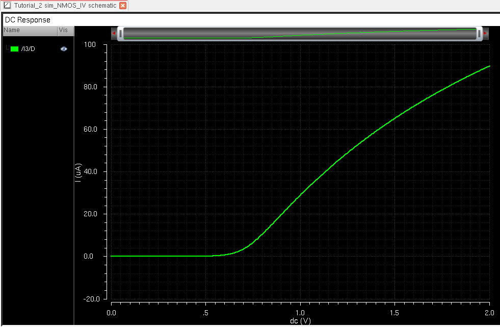
schematic for simulating ID v. VGS of an NMOS device for VDS = 100 mV
where VGS varies from 0 to 2 V in 1 mV steps. Again use a 6u/600n
width-to-length ratio.

Simulation
Creating the PMOS Schematic for IV Curve
1)Similarily to what we did for NMOS, using the 3pins pmos we created create the schematic below.
- A
schematic for simulating ID v. VSD (note VSD not VDS) of a PMOS device
for VSG (not VGS) varying from 0 to 5 V in 1 V steps while VSD varies
from 0 to 5 V in 1 mV steps. Use a 12u/600n width-to-length ratio.

Simulation (Note: bes sure to change the variable from VGS to VSG in the ADE)

- A
schematic for simulating ID v. VSG of a PMOS device for VSD = 100 mV
where VSG varies from 0 to 2V in 1 mV steps. Again, use a 12u/600n
width-to-length ratio.

Simulation

- Lay
out a 6u/0.6u NMOS device and connect all 4 MOSFET terminals to probe
pads (which can be considerably smaller than bond pads [see MOSIS design rules] and directly adjacent to the MOSFET (so the layout is relative small).
- Show your layout passes DRCs.
- Make a corresponding schematic so you can LVS your layout.
Lay out

Schematic

LVS Result to make sure the net-list match.

- Lay out a 12u/0.6u PMOS device and connect all 4 MOSFET terminals to probe pads.
- Show your layout passes DRCs.
- Make a corresponding schematic so you can LVS your layout.
Lay out

Schematic

LVS to make sure the netlist match

Finally, make sure the back up your work by typing tar -cvf compbackup.tar CMOSedu/.
This will create a tar file with all the project and homework saved. In
place of "date" type in the date creating the backup. Unce the backup
has been created type gzip backupdate.tar. This will create a .tar.gz file witch is significantly smaller.
Return to EE 421L Labs