


Lab 5 - EE 421L
Design, Layout, and Simulation of a CMOS Inverter
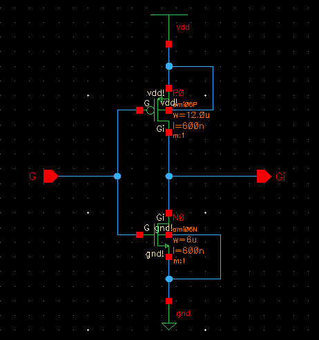
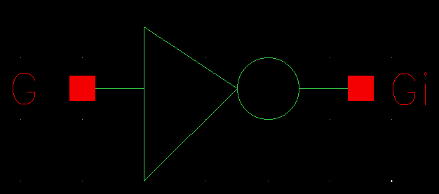
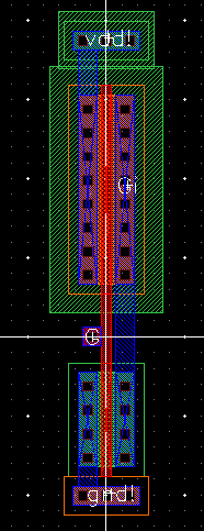
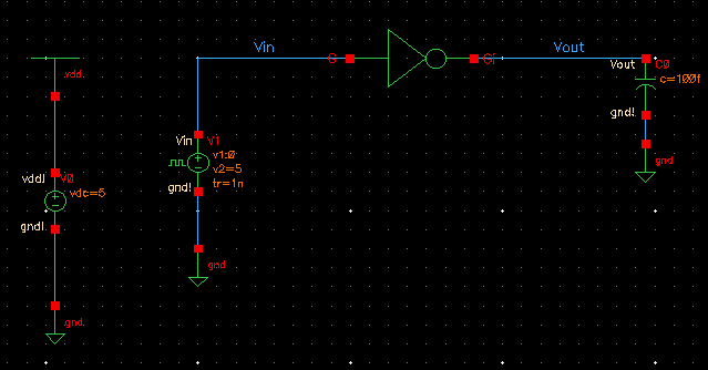
The objective of this lab is create shematics, layouts and simulations of CMOS inverters in the C5 Process.
1. The (12u/6u) Inverter
| Design |
Verification |
|
| Schematic |
 |
 |
| Symbol |
 |
 |
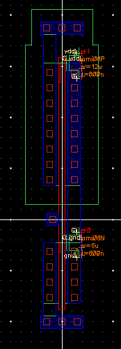
| Layout |
 |
 |
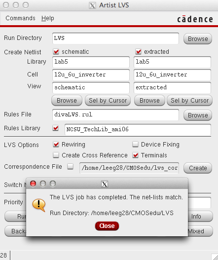
| Extracted |
 |
 |
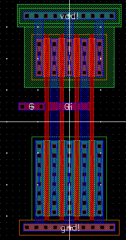
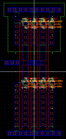
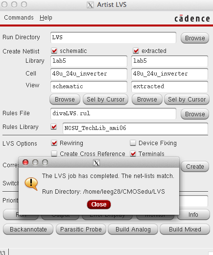
2. The (48u/24u) Inverter
| Design |
Verification |
|
| Schematic |
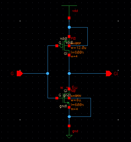 |
 |
| Symbol |
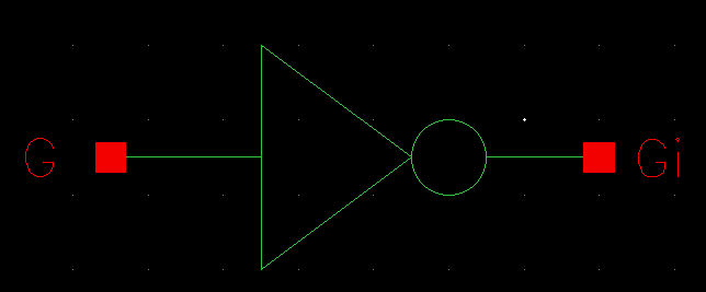 |
 |
| Layout |
 |
 |
| Extracted |
 |
 |
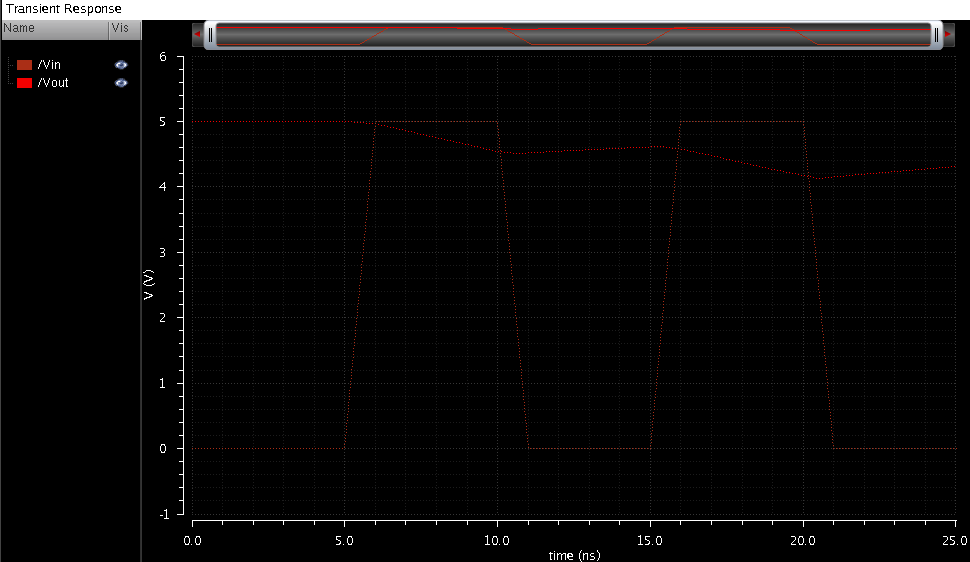
Simulations
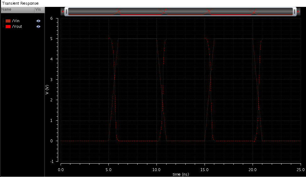
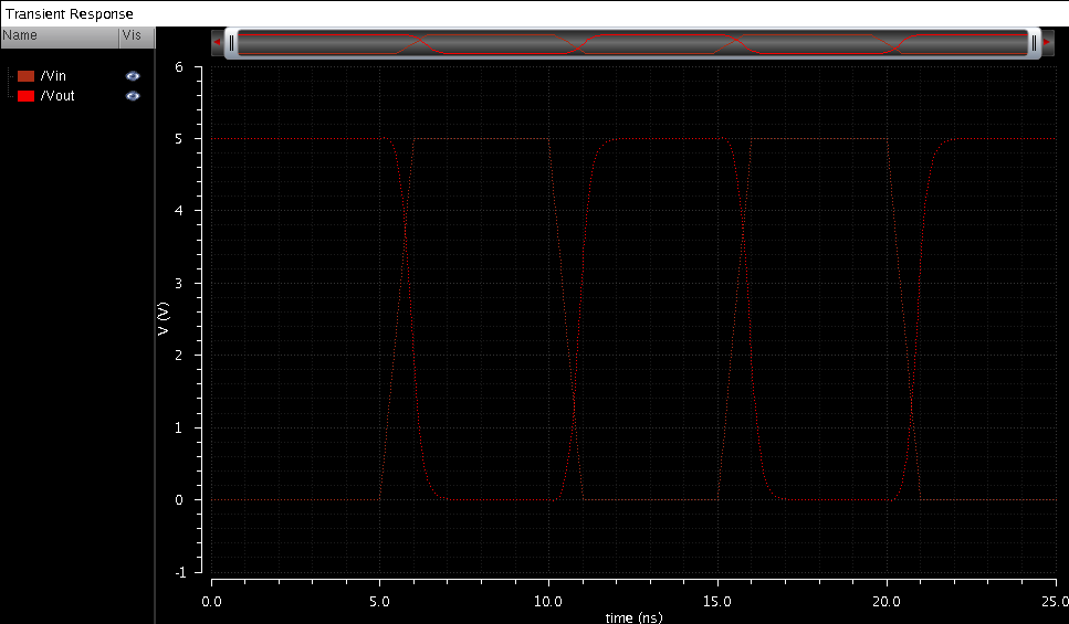
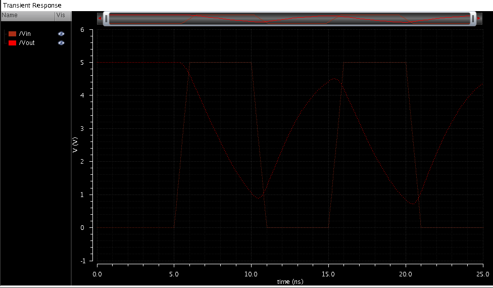
The
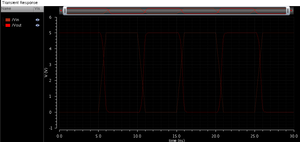
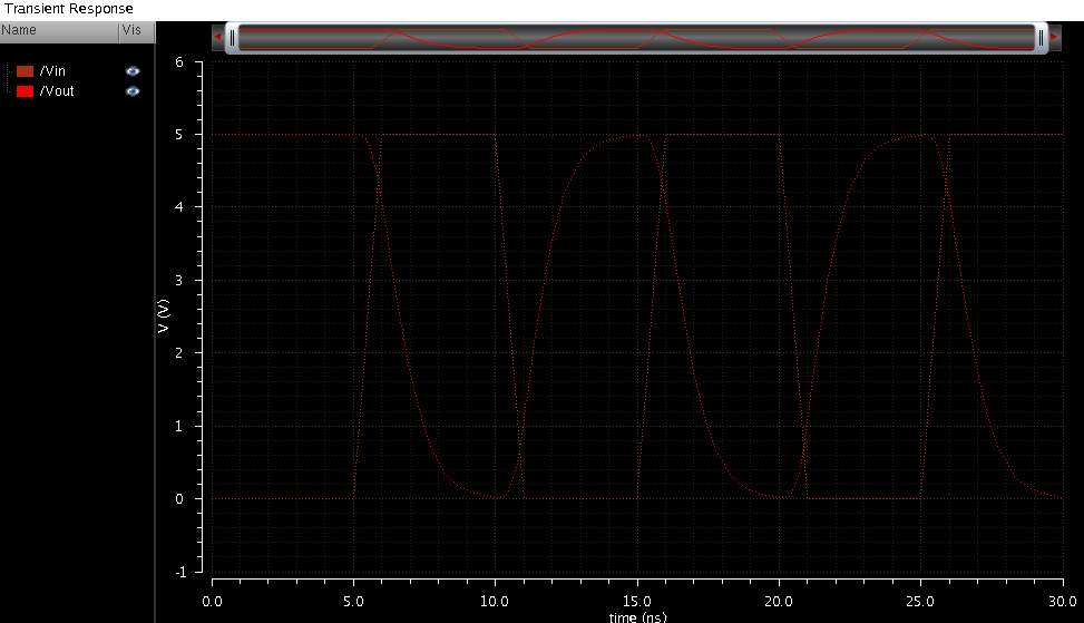
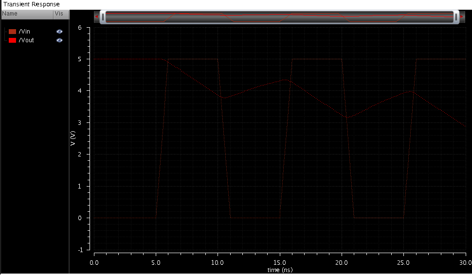
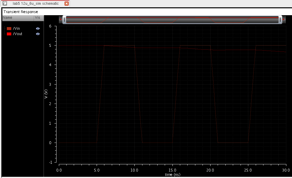
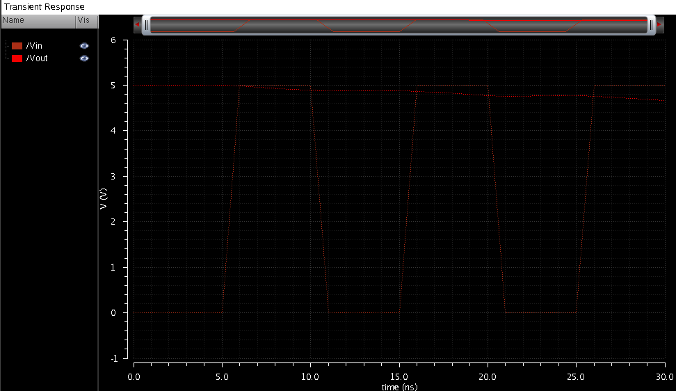
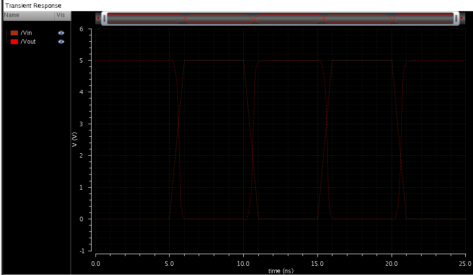
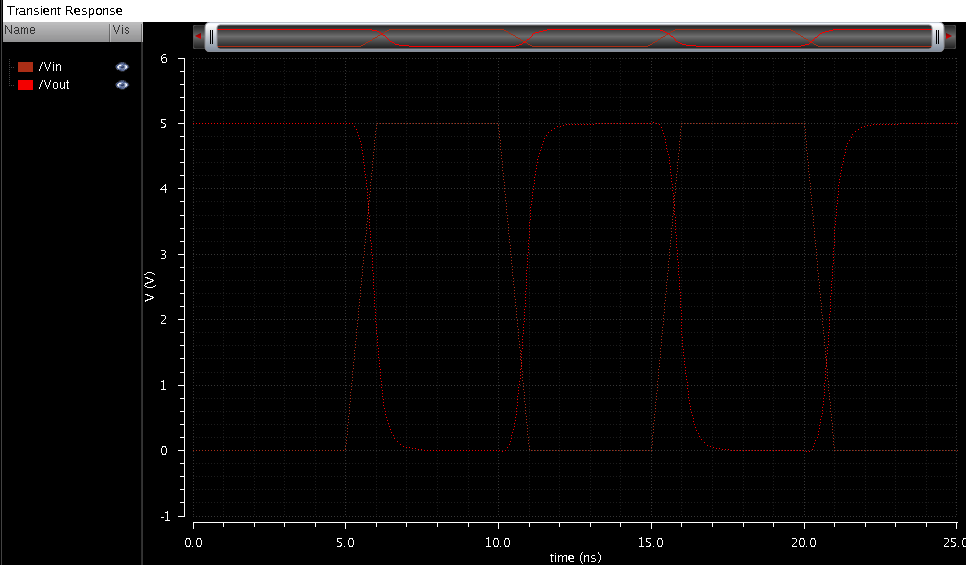
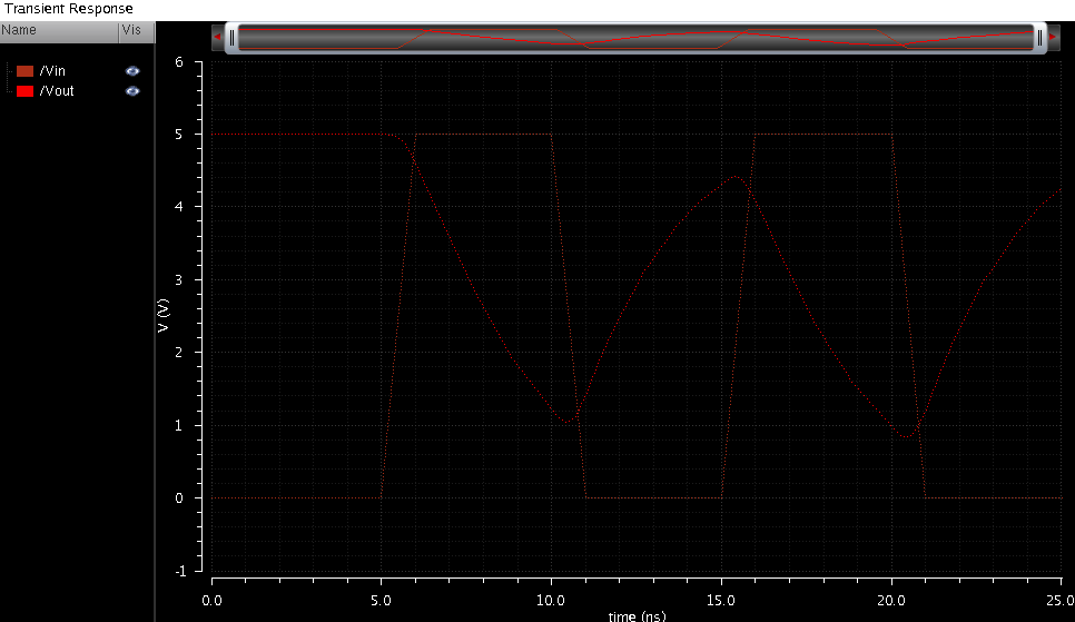
one thing that is apparent in all simulations of either inverter is
that when the capacitive load is increased that the output signal of
the inverter becomes more distorted, this is due to the delay of the
circuit. The greater the capacitive load, the greater the delay. These simulations show the effects of parasitic
capacitances and why we should always have them in mind when during
circuit design and layout. These plots also show that increasing the width of a mosfet can improve performance by reducing delay.
The
last two tables use Simulink instead of Spectre to simulate the
inverters. What UltraSim gains in speed it lacks in accuracy, most
important to remember UltraSim is only capable of transient analysis.
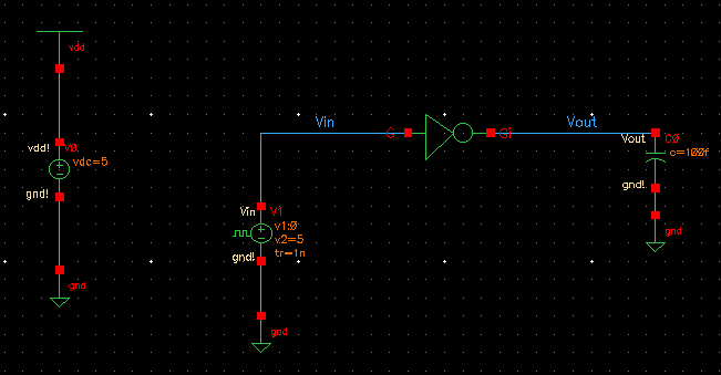
3. The (12u/6u) Inverter Simulations (Using Spectre)
| Capacitive Load |
Plot |
| 100f |
 |
| 1pf |
 |
| 10pf |
 |
| 100pf |
 |
| Capacitive Load |
Plot |
| 100f |
 |
| 1pf |
 |
| 10pf |
 |
| 100pf |
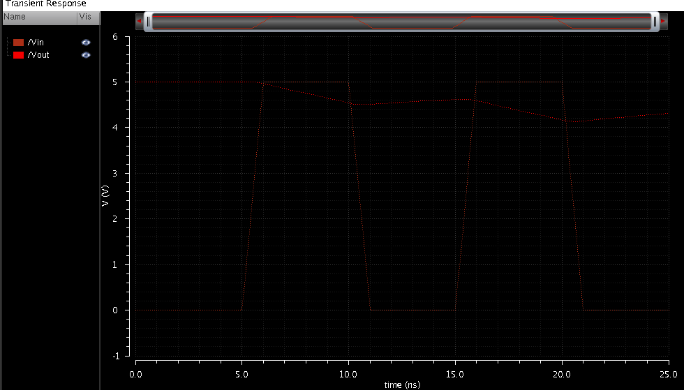 |
5. The (12u/6u) Inverter Simulations (Using Ultrasim)

| Capacitive Load |
Plot |
| 100fF |
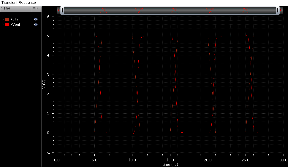 |
| 1pF |
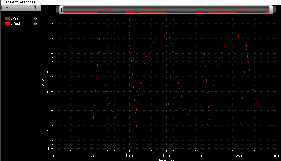 |
| 10pF |
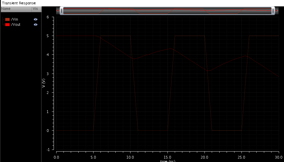 |
| 100pF |
 |
5. The (48u/24u) Inverter Simulations (Using Ultrasim)

| Capactive Load |
Plot |
| 100fF |
 |
| 1pF |
 |
| 10pF |
 |
| 100pF |
 |
