Lab 4 - EE 421L
Authored
by Gerald Lee
leeg28@unlv.nevada.edu
October 4, 2014
IV Characteristics and Layout of NMOS and PMOS Devices in ON's C5 Process
The objective of this lab is create shematics, layouts and simulations of NMOS and PMOS devices in the C5 Process.
NMOS Schematics and Simulations
1. ID v. VDS of an NMOS device for VGS varying from 0 to 5 V in 1
V steps while VDS varies from 0 to 5 V in 1 mV steps. (W/L = 6u/600n)

Draft the following schematic, set the voltage source tied to the gate to "VGS" and the voltage source tied to the drain to 0.

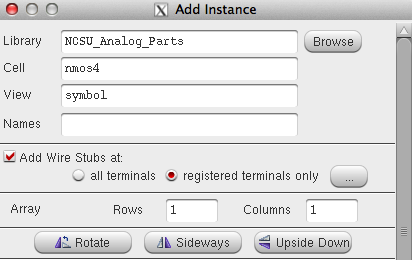
You can find the NMOS used for this schematic under the Library: "NSCU_Analog_Parts" and under the Cell:nmos4.
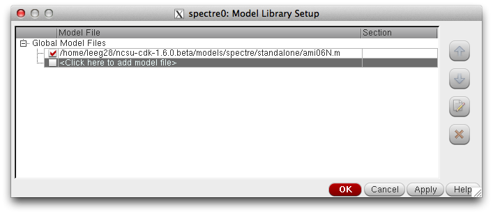
Launch the ADE, ensure the the simulation using the corresponding model file:

Create "VGS" as a design variable. Under Variables -> Edit set the following:

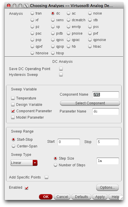
Under Analyses -> Choose set the following:

These settings will sweep "VDS" from 0 to 5V using 1 mV steps.
After checking component parameter, press the "Select Component" Button
and choose the voltage source tied to the drain of the NMOS.
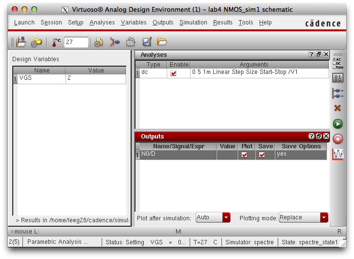
Navigate the following path and choose drain node of the NMOS to be plotted: Outputs -> To Be Plotted -> Select on Schematic
Simulation setting should now resemble the following:

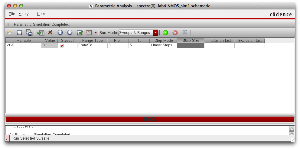
Under Tools -> Parametric Analysis set the following:

These settings will sweep "VGS" from 0 to 5V using 1V steps.
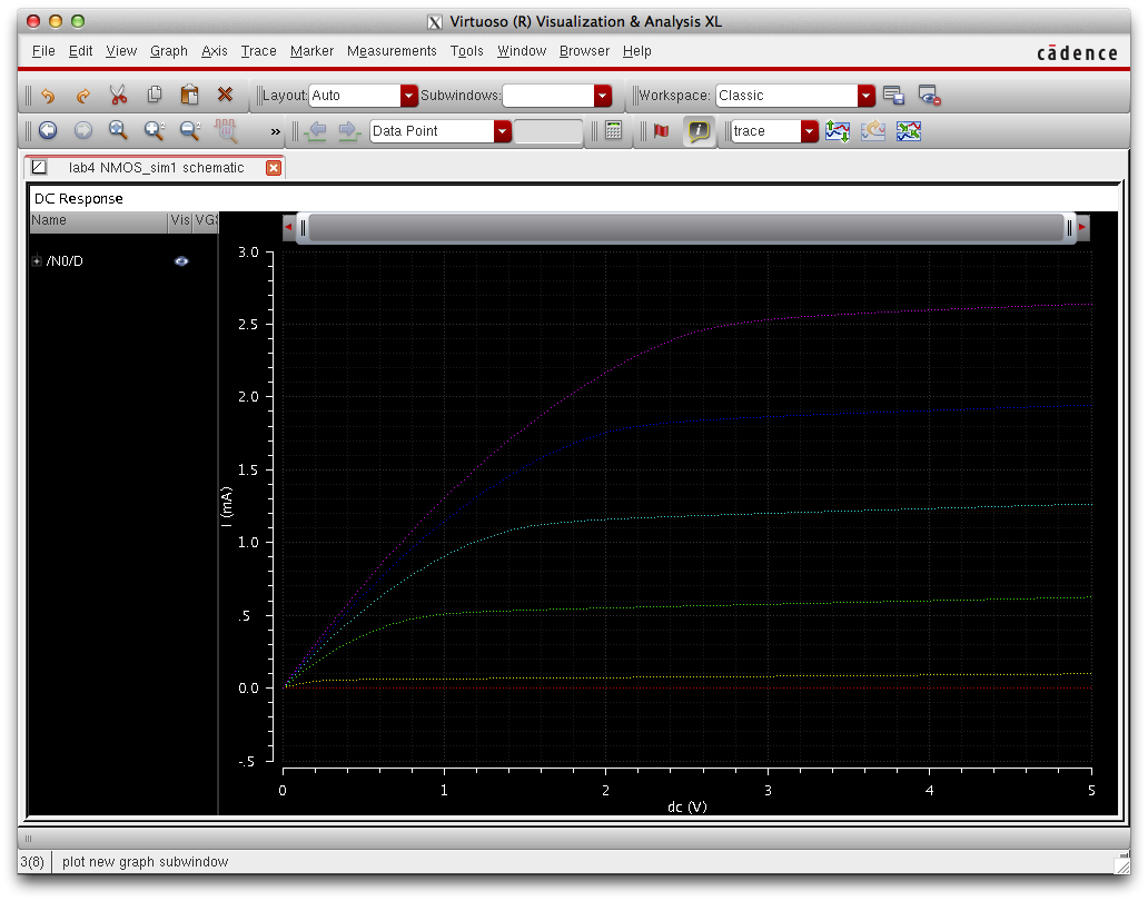
Press play to reveal final simulation.
ID v. VDS (NMOS 6u/600n)

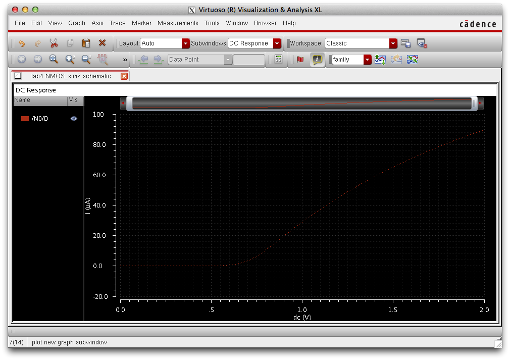
2. ID v. VGS of an NMOS device for VDS = 100 mV where VGS varies from 0 to 2 V in 1 mV steps

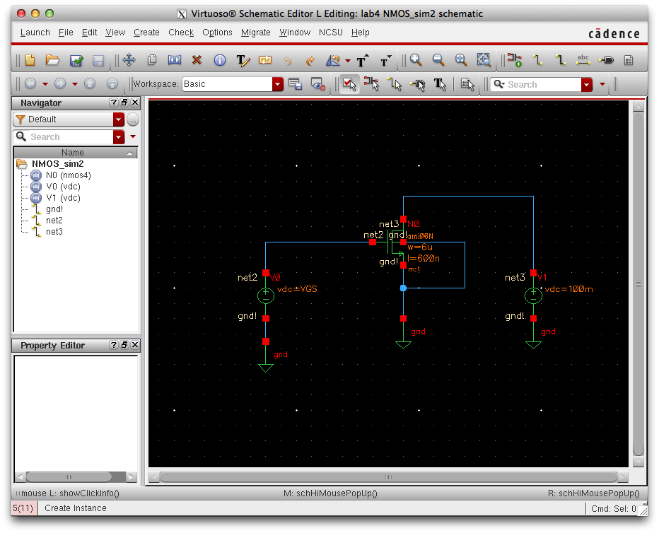
Draft the following schematic, note we can set VDS to 100mV since it is not being swept.

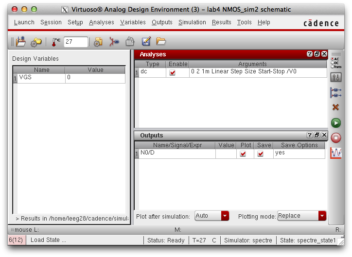
Open the ADE and set the following simulation settings using previous steps described above.
We can see from the image above that VGS is being swept from 0 to 2V using 1mV steps.
Since there is only one variable being swept it is not necessary to use parametric analysis.
Hit play to reveal the following simulation.
ID v. VGS (NMOS 6u/600n)

PMOS Schematic and Simulations
The explanation of PMOS schematics and simulations will be less detailed as they are very similar to steps above.
Be sure to set the correct model for PMOS simulations, "ami06P".
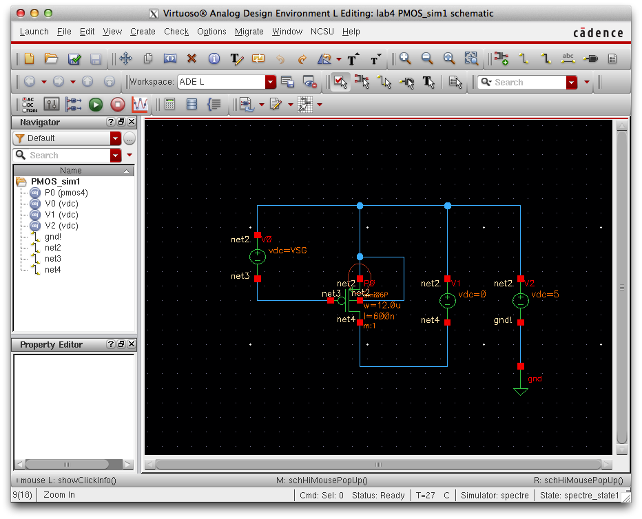
1. ID v. VSD of a PMOS device for VSG varying from 0 to 5 V in 1 V
steps while VSD varies from 0 to 5 V in 1 mV steps. (W/L = 12u/600n)

Draft the following schematic, label voltage sources accordingly.

Launch the ADE and set the following simulation settings.
From the following image above we can see that VSD is being swept from 0 to 5V using 1mV steps.
Choose the source node on the schematic as the output to be plotted.

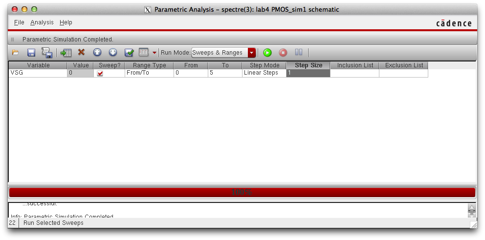
Set parametric analysis settings, from the following image above VSG will be swept from 0 to 5V using 1V steps.
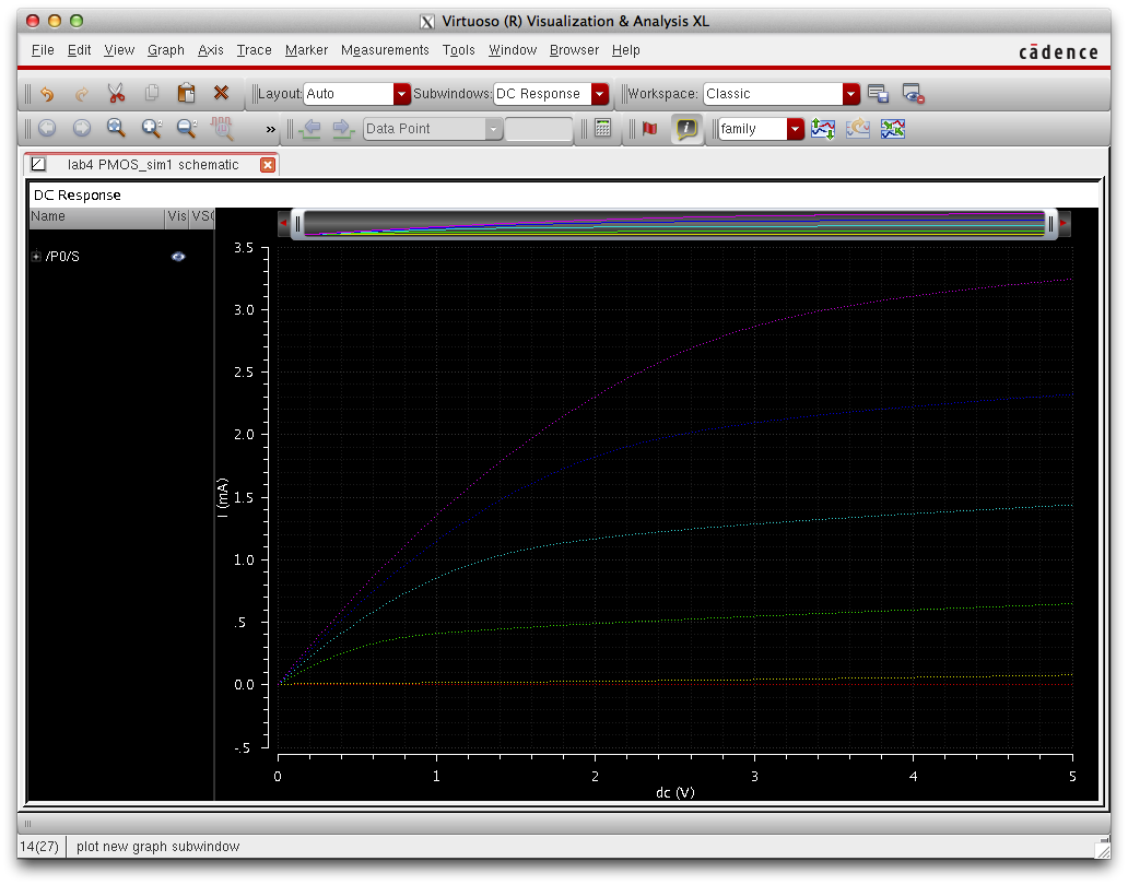
Press play to reveal the following schematic.
ID v. VSD (NMOS 12u/600n)

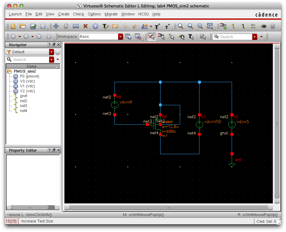
2. ID v. VSG of a PMOS device for VSD = 100 mV where VSG varies from 0 to 2 V in 1 mV steps. (W/L = 12u/600n)

Draft the following schematic.
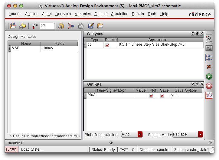
Open the ADE set the following simulation setting:

Notice that VSD is set to 100mV while VSG is being swept from 0 to 2V using 1mV steps.
Choose the source node of the PMOS as output.
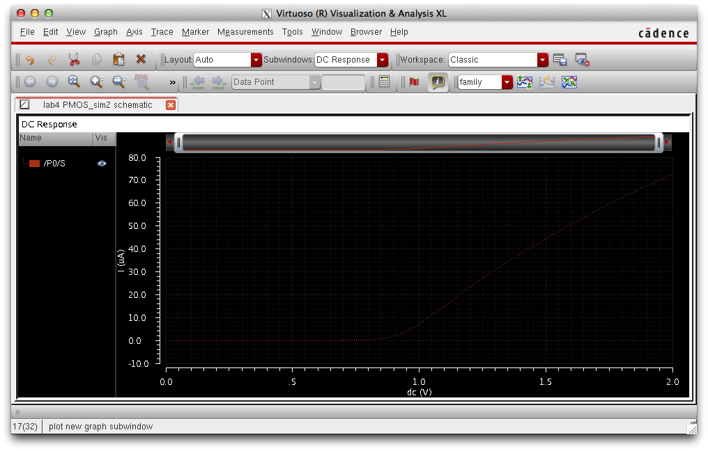
Press play to reveal the following schematic.
ID v. VSG (NMOS 12u/600n)

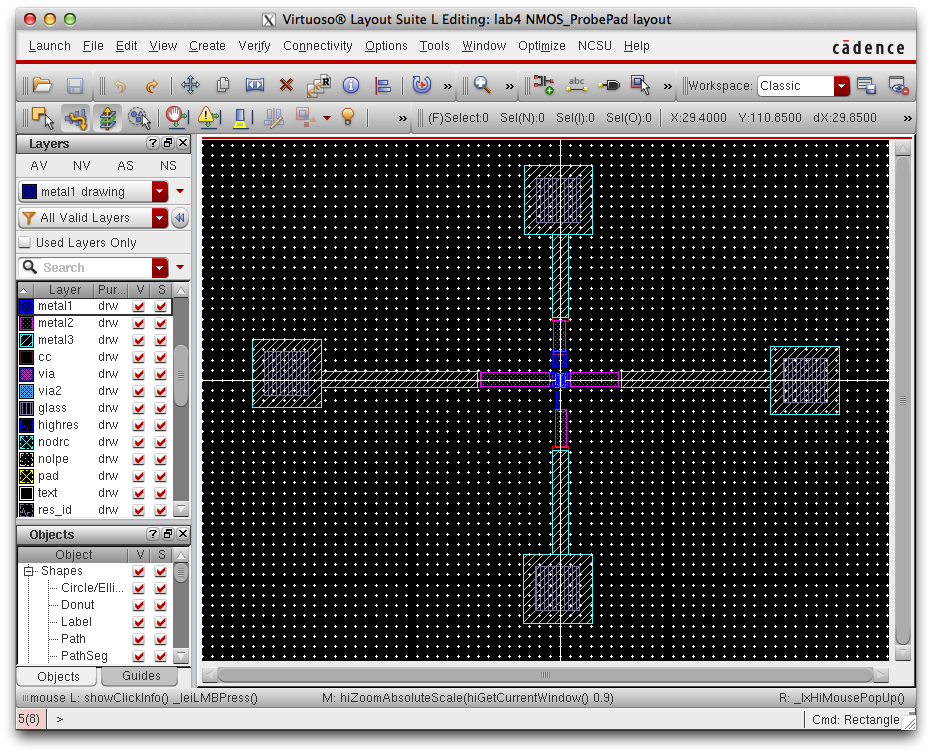
NMOS w/ Probe Pad Schematic & DRC


NMOS w/ Probe Pad Layout & LVS


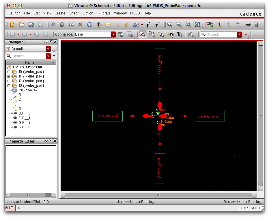
PMOS w/ Probe Pad Schematic and DRC


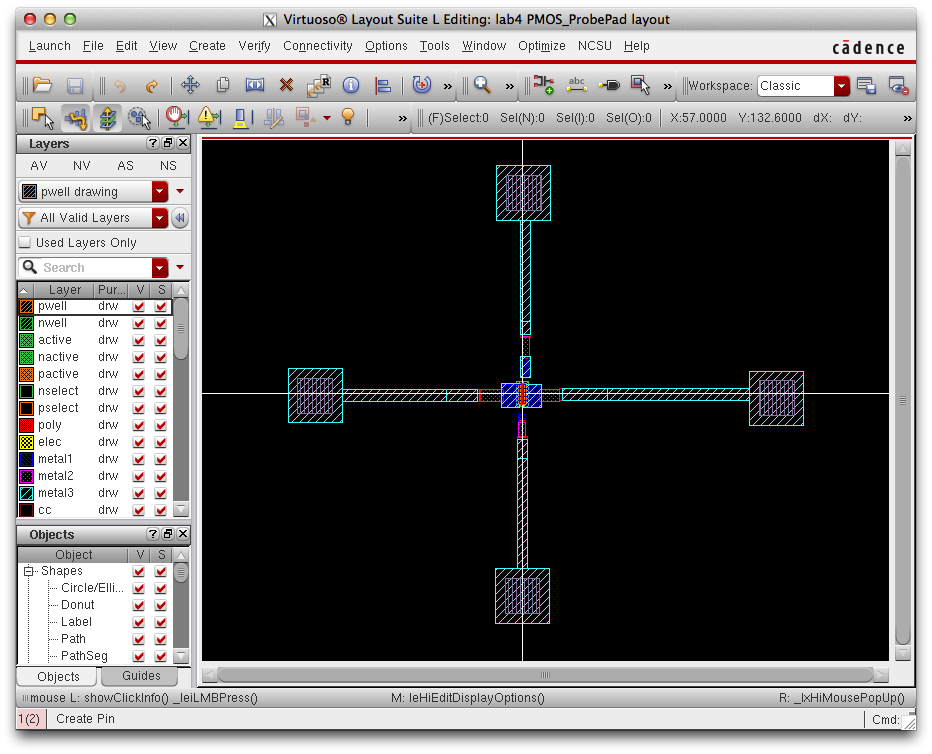
PMOS w/ Probe Pad Layout

Back-up through personal hard drive is shown below:

This concludes the lab design files for this lab can be found here.

