Lab 3 - EE 421L
Layout of a 10-bit Digital to Analog Converter
The objective of this lab to create a layout for the 10-bit digital to analog converter created in within the previous lab.
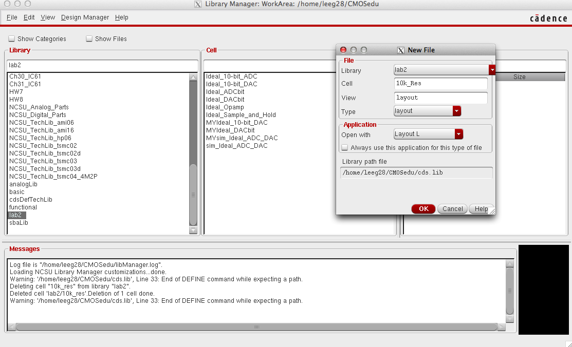
Create a new cell view for your 10-bit DAC Layout

Layout N-Well Rectangle
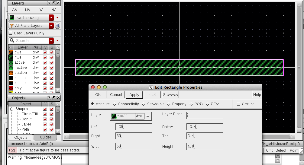
Choose
the N-Well layer and layout a rectangle of N-Well with Length= 60 and
Width = 4.8, DRC your layout to check design rules.
Choosing Resistor Values:
Resistance can be calculated by using the formula:
Rtotal = Sheet Resistance * (Length/Width)
Values
for sheet resistance can be found within the design rules of the
process one is using, design rules for the C5 process can be found here.
Clicking the link above shows that the sheet resitance of N-Well = 800 Ohms/Square

Because
the total resistance = 10k and the sheets resistance of N-Well =800, by
using a length of 4.8 we can solve for Length = 60.
Design rules to remember when sizing Resistors:
1. Be sure fit within grid size specifications, in the C5 process
Lambda = .3 microns, therefore width and height of layouts must all be
divisible by .3
2. Minimum n-well spacing must be at least 12*Lambda or in the C5 process 3.6 microns.
Add Metal Connections to the ends of the N-Well Resistor
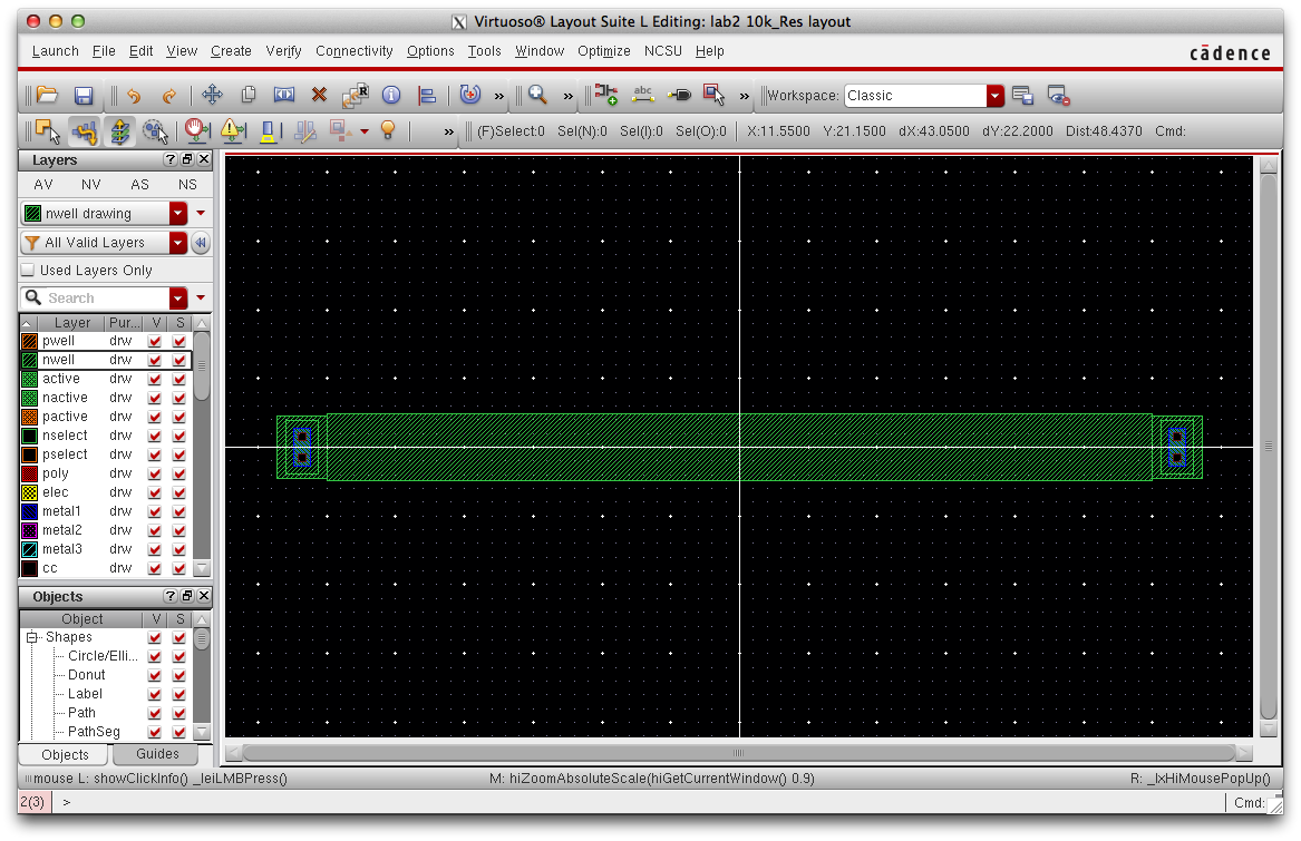
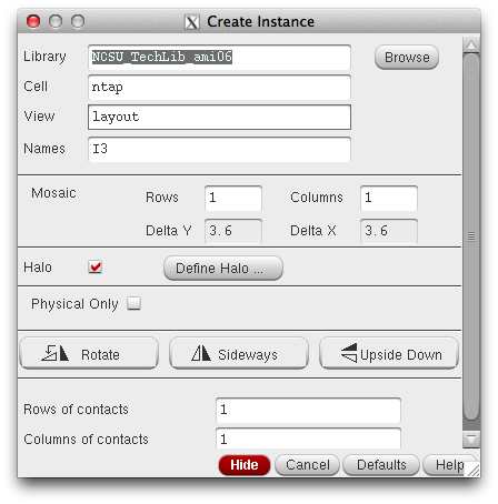
Use the Library above to add connections to either end of the N-well Resistor.
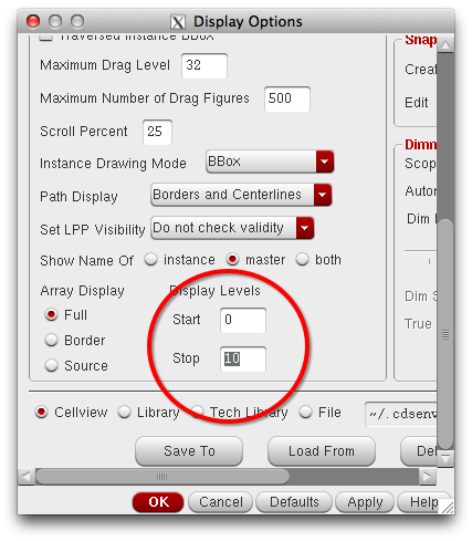
*Pressing
E will show the display options, make sure to adjusted the display
levels to the paramters above to show the Ntap layout.
Add Pins to the Left and Right of the N-Well Resistor
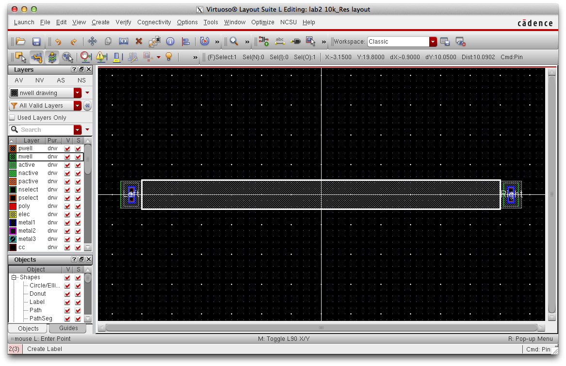
Navigate to Create -> Pin to Add a Pin Label
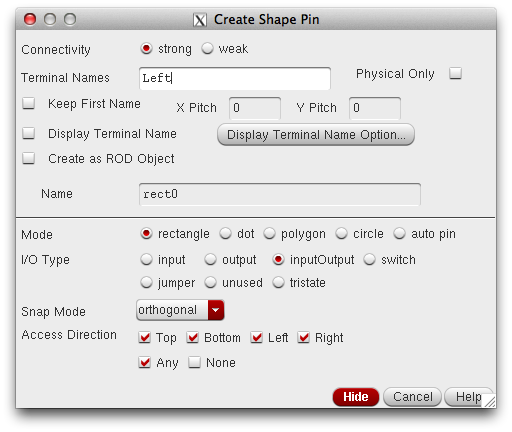
*Be sure to check "Display Terminal Name" to show Pin Names in the schematic.
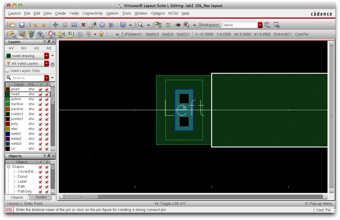
When creating a pin, create a rectangle over the ntap and place the label in the middle of the ntap.
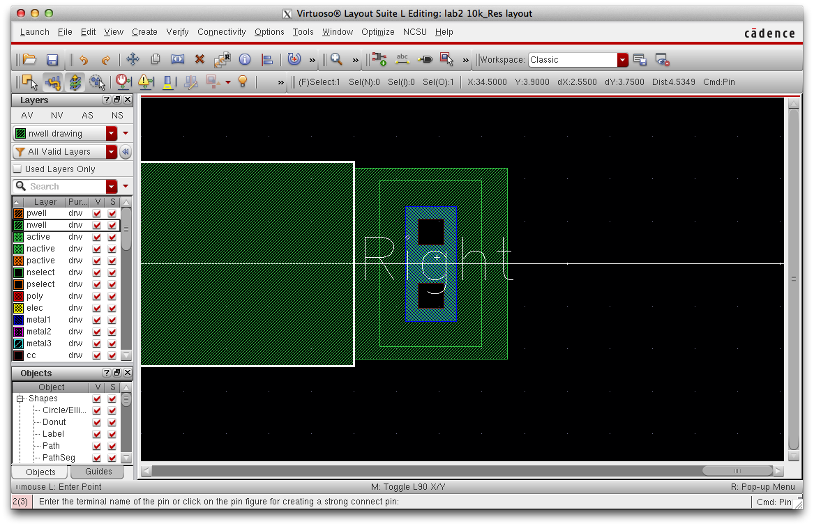
Do the same for the right side of the N-Well resistor.
Apply the res_ID layer over the N-Well
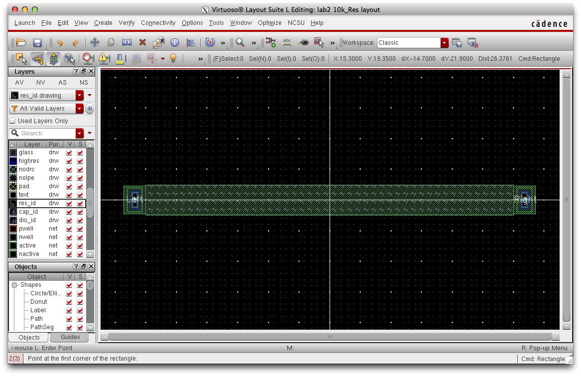
Layout the res_id layer over the n-well to identify that the component is a resistor.
Extract the Layout
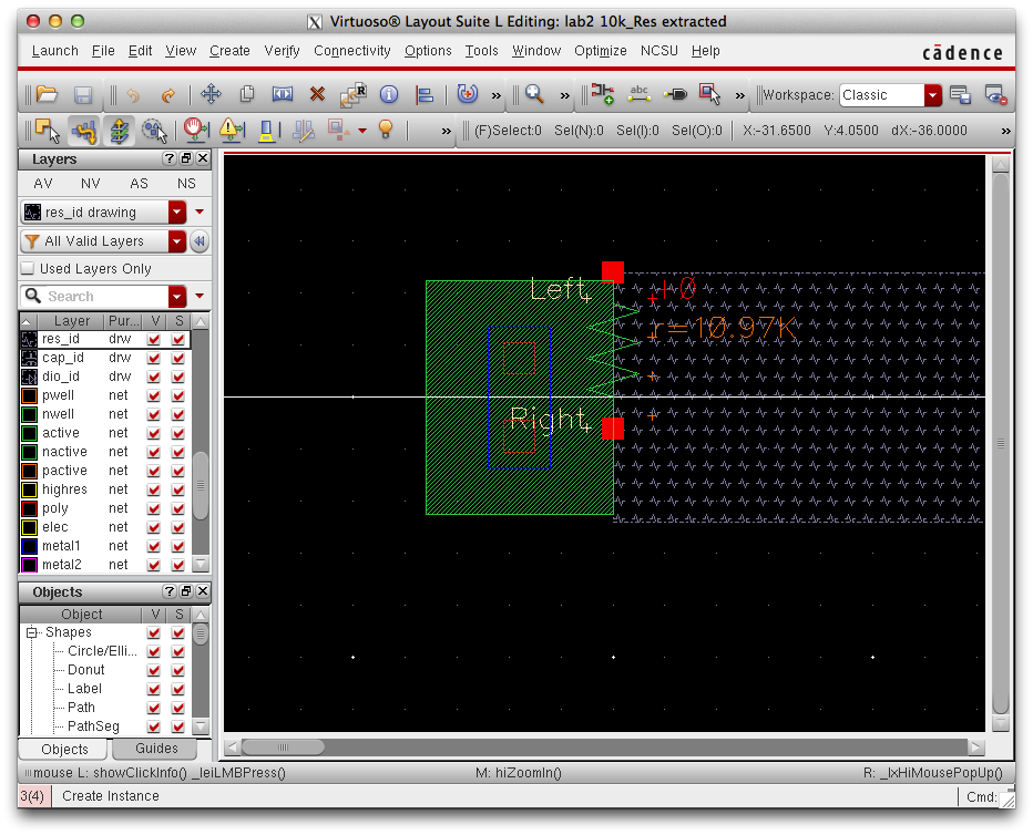
Save your work, DRC to check design rules and extract your layout.
Verify -> Extract
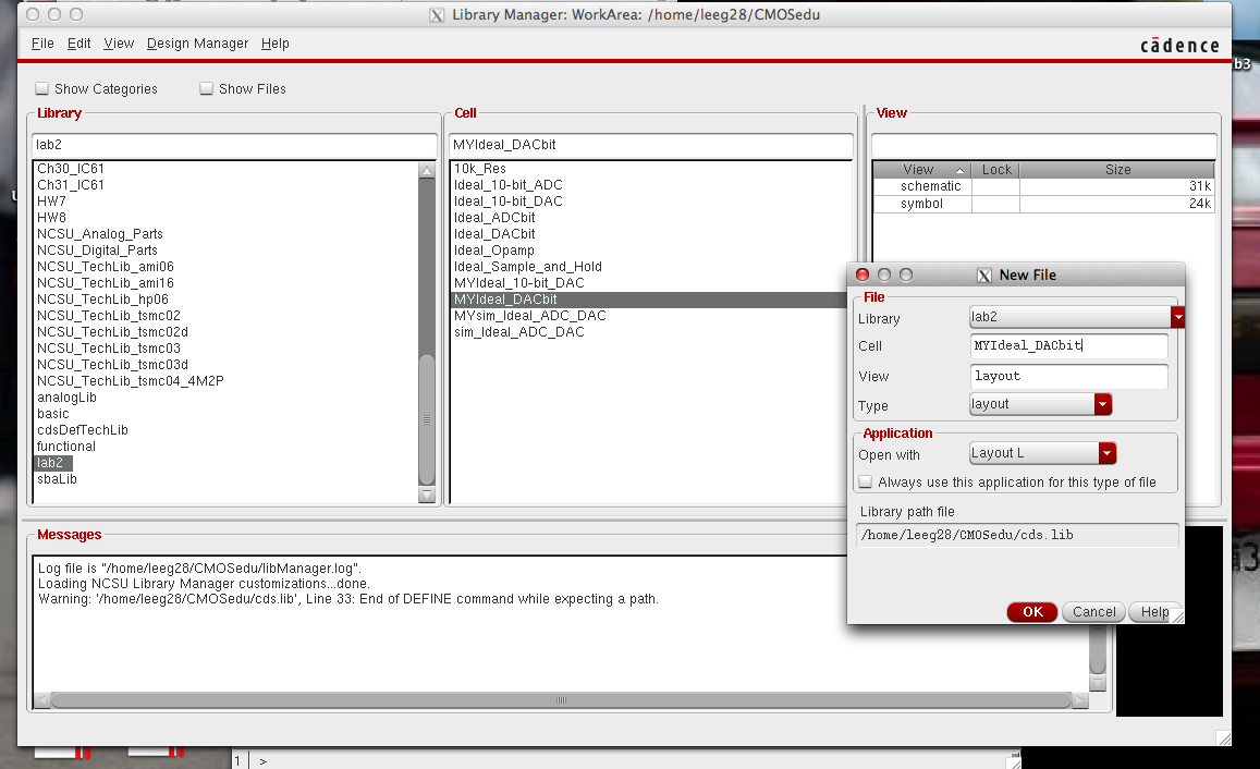
Create a new layout cell view under "MyIdeal_DACbit"
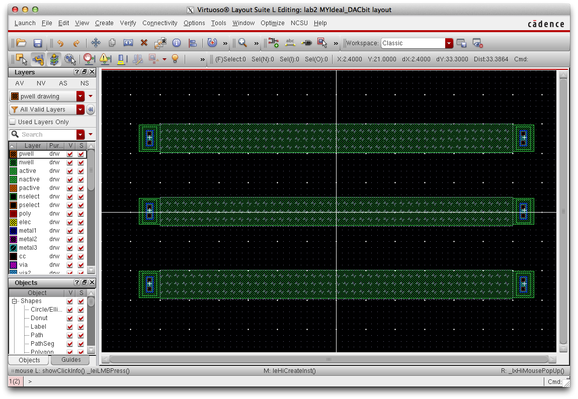
Press "I" to add an instance of the 10k_res layout you created. DRC your layout agrees with design rule specifications.
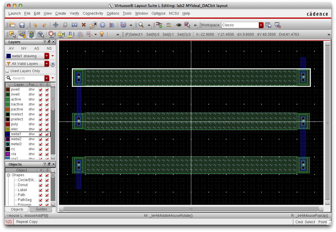
Choose the metal1 layer and connect the resistors together (see above) using the key button "R" or rectangle.
Add Pins to the Layout
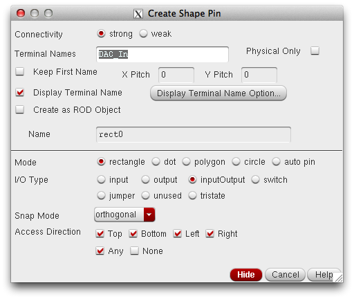
Navigate here to add pins:
Create -> Pin
*When adding pins be sure to check "Display Terminal Name" under the Create Shape Pin Window
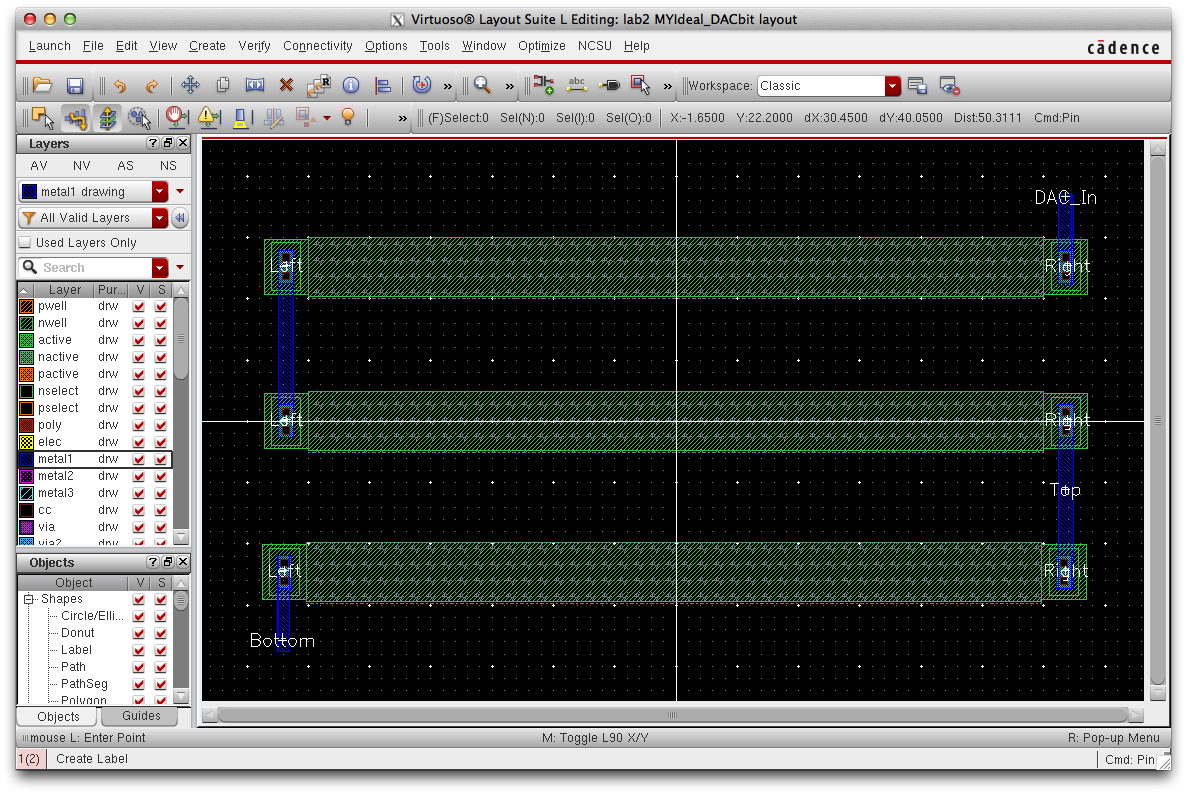
Here is my layout with all necessary pins, be sure that pin names agree with those used in your schematic.
Extract and LVS
Extract this layout using the same procedures for extracting as before.
DRC and Ensure there are no errors (see below).

To LVS navigate here:
Verify -> LVS
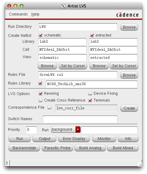
The
"Artist LVS" window will show. Under schematic and extracted, browse
for your schematic and extracted designs to have the layout compared.
If everything is done correctly, you will receive a notification that the LVS was successful (see below).
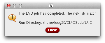
LVS Output here:
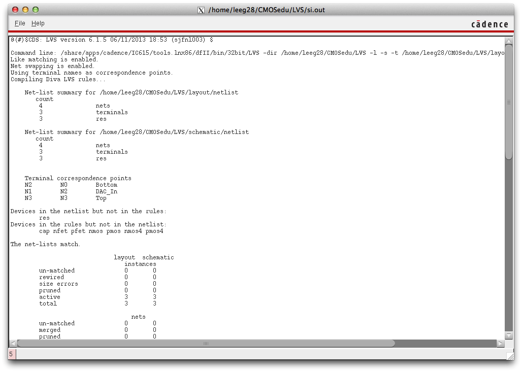
This concludes Lab 3, design files can be found here.
Lab 3 Back-Up
