Lab 2 - ECE 421L
Authored
by Gerald Lee
leeg28@unlv.nevada.edu
September 21, 2014
Pre-Lab
Download lab2.zip, place this file in your CMOSedu directory.
Once in your CMOSedu directory, Unzip the file using the command:
unzip lab2.zip
Modify your cds.lib file to include the lab 2 directory by this command:
DEFINE lab2 $HOME/CMOSedu/lab2
Start Cadence by entering this command in your CMOSedu directory
virtuoso &
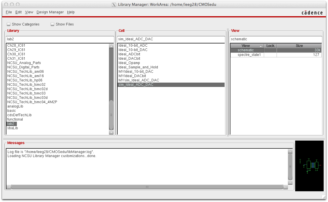
Using your library manager, open sim_Ideal_ADC_DAC (schematic) under
lab2 -> sim_Ideal_ADC_DAC -> schematic

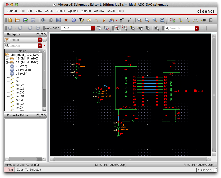
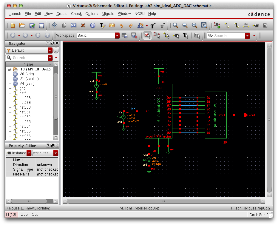
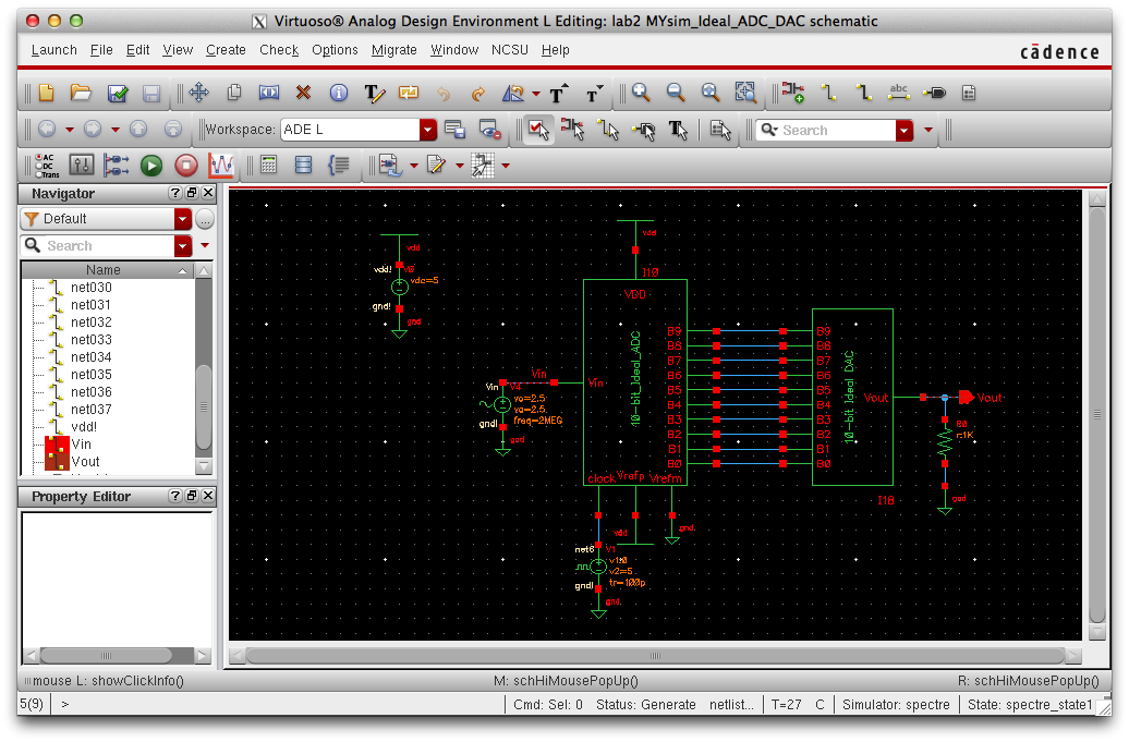
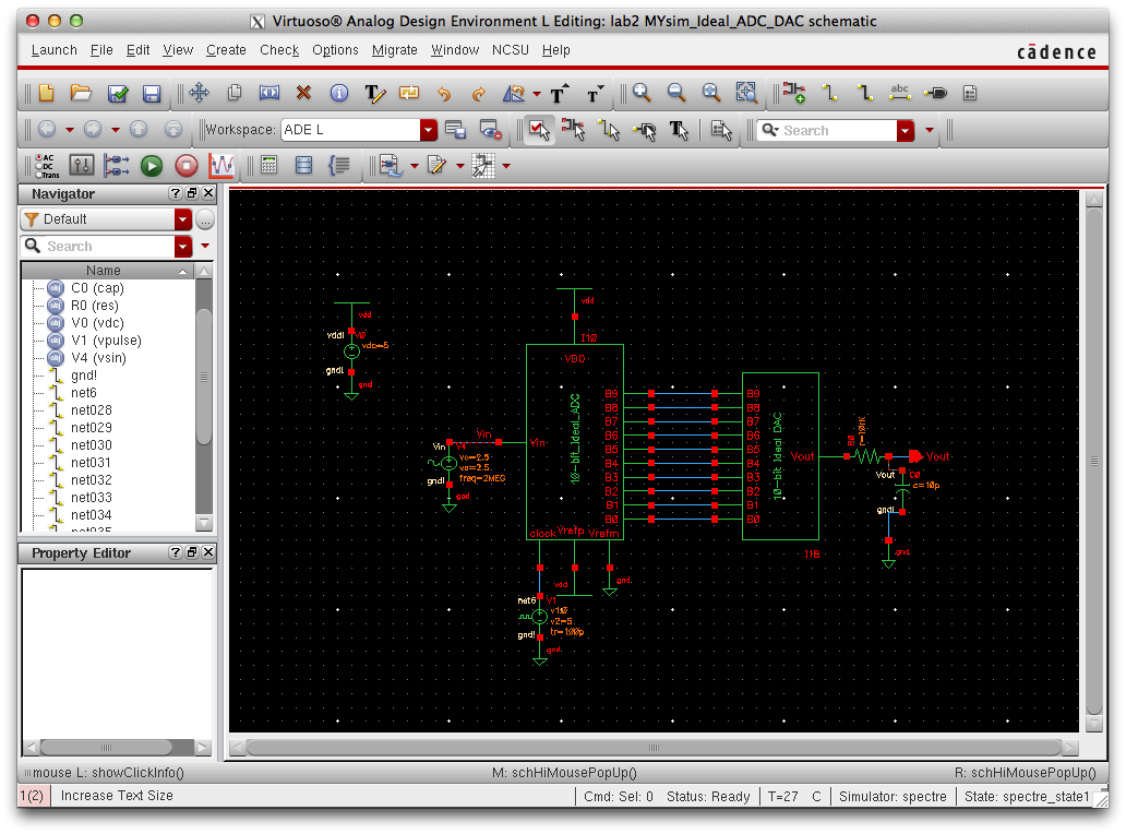
Upon opening you will see the following schematic:

Launch the simulator:
Launch -> ADE L
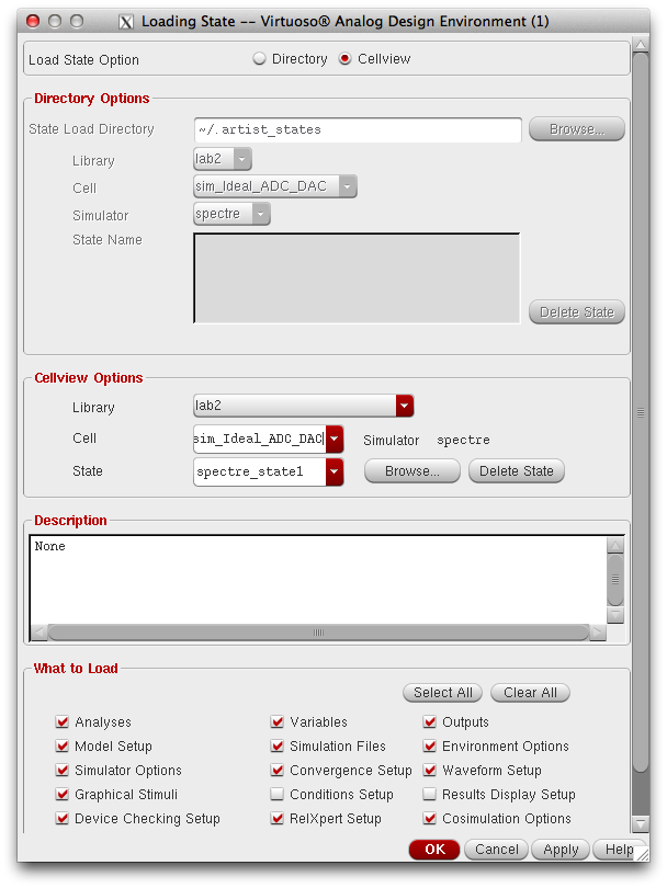
Load the cell view:
Session -> Load State (Choose Cell View then Hit OK)

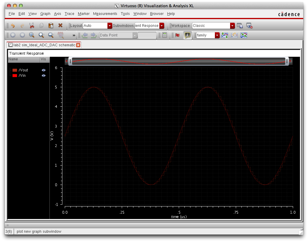
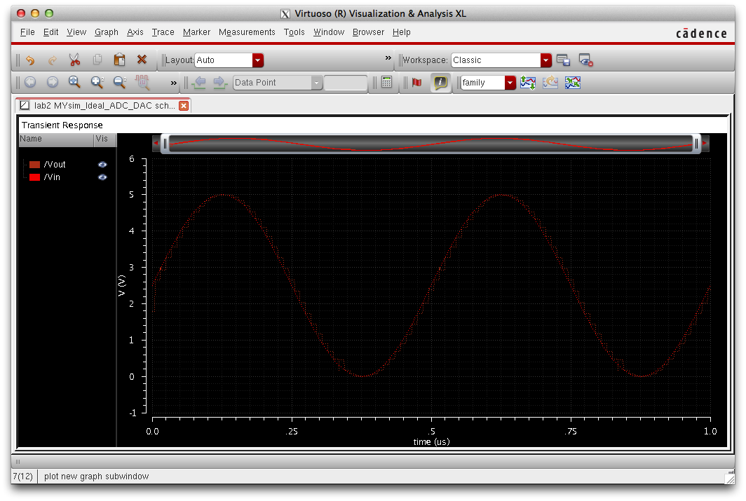
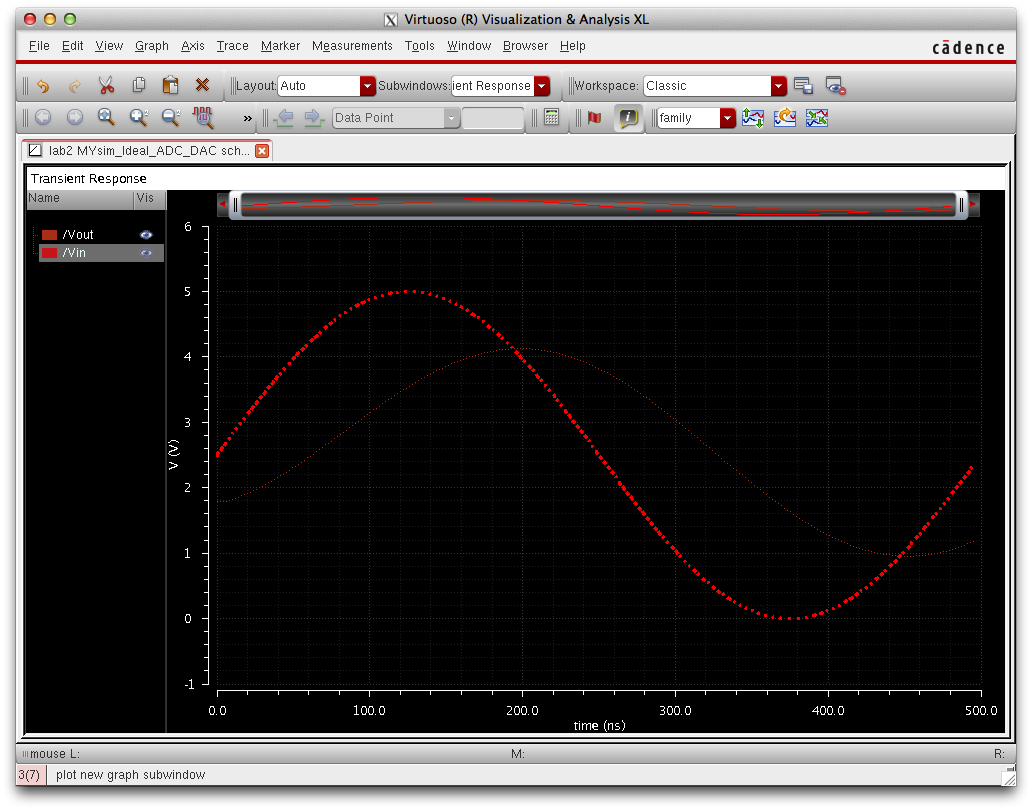
Run the simulation and observe the plot below:
This
plot shows the analog signal (Vin) and the Analog signal after
conversion (Vout) , notice that the waveform has become jagged due to
the DAC.

Note: Plot color and thickness can be adjusted by right clicking on the node name to the left of the plot.
LSB
stands for least significant bit and shows the minimum level which an
ADC can convert, the formula for calculating LSB shown below:

For our DAC LSB = 4.88 mV, LSB= 5/2^10
Post-Lab
The design of a 10-bit DAC using an n-well R of 10k:
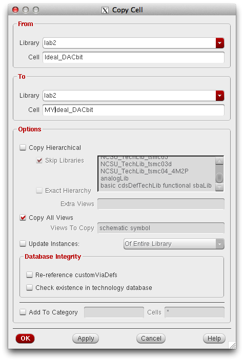
Copy Ideal_DACbit using the library manager, in the image below I named the new cell "MYIdeal_DACbit", open the new cell.

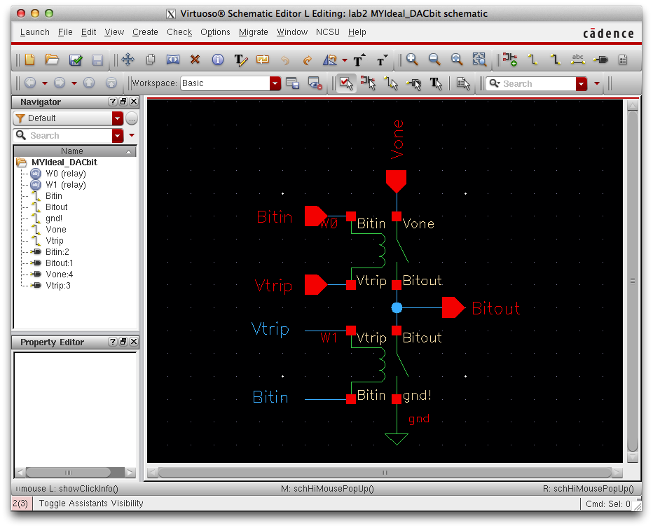
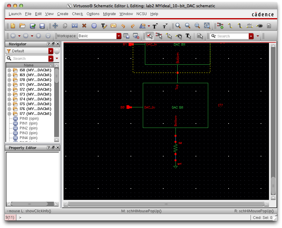
Upon opening, this schematic will be shown:

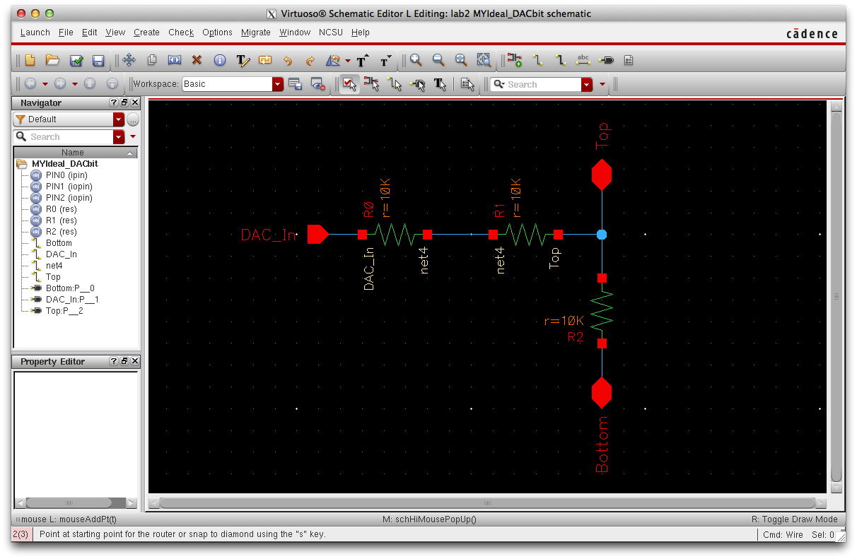
Delete the entire schematic, and create the schematic seen below.
Use these hot keys to make this process easier (I= "Instance", P= "Pin", W="Wire")

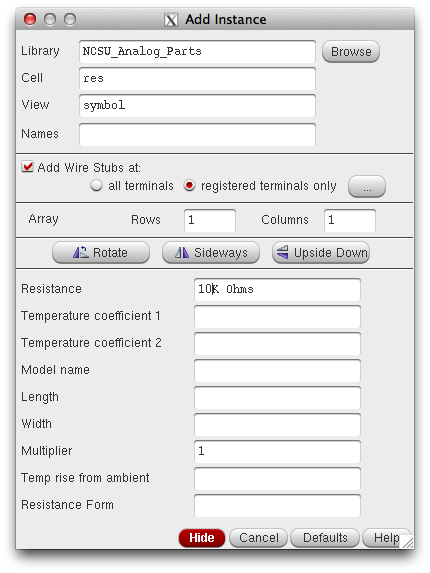
Please Note: Resistors can be found under this library:

Check and save your work to ensure there are no errors.
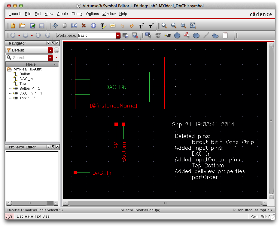
Next we will edit the symbol, corresponding to the schematic we just created.
Using the Library Manager, follow the follwing path to open MYIdeal_DACbit
lab2 -> MYIdeal_DACbit -> symbol
Upon opening this symbol will appear:

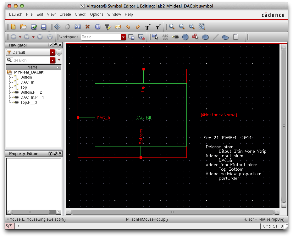
Edit the symbol to the folowing:

Check and save your work to ensure there are no errors!
Next will modify the 10 bit DAC Schematic:
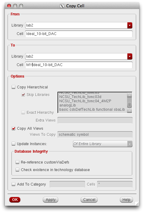
Using the library manager copy Ideal_DACbit cell to a new cell. In the image below I named the new cell "MYIdeal_DACbit".
Open the schematic view of the new cell.

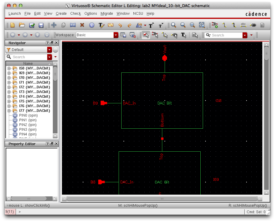
After opening the schematic, delete all components and use the hot key "I" to add the 10 bit DAC previously created.
From the top to bottom, name each DAC input B9-B0. Place a Vout pin on the top DAC and tie the bottom pin of the
last DAC to a 10k resistor and ground.


Next we will edit the symbol corresponding with the 10-bit DAC just created.
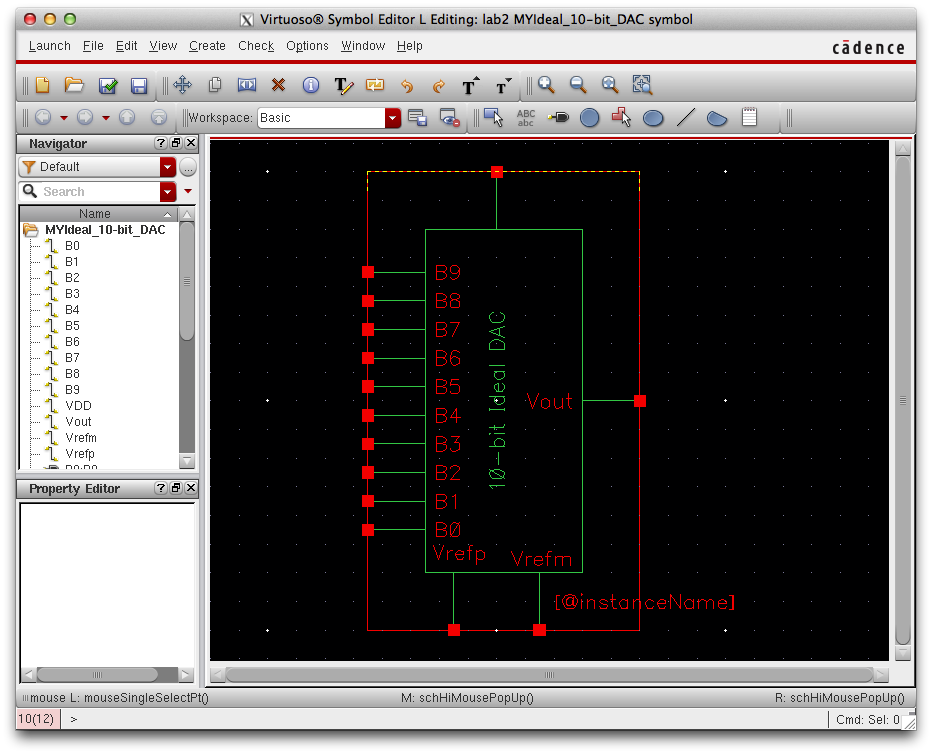
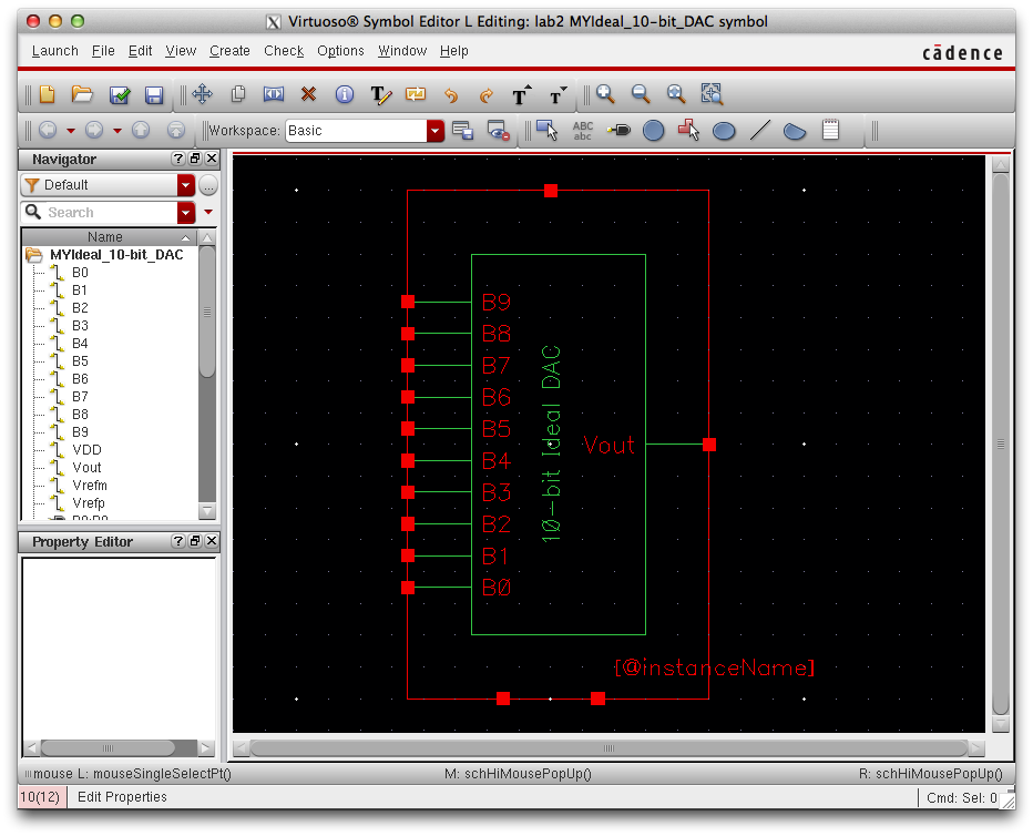
Use the library manager to open the 10-bit DAC symbol, you will see the following:

Change the symbol to following and check and save your work to ensure there are no errors

Copy the sim_Ideal_ADC_DAC and open the file, use I= "Instance" add the
10 bit DAC recently created with the one already in place.

Simulating the 10-bit DAC
To run the simulator: Launch -> ADE L
To Select Outputs: Outputs -> To be plotted -> Select on Schmatic (Choose Vin and Vout on schematic)
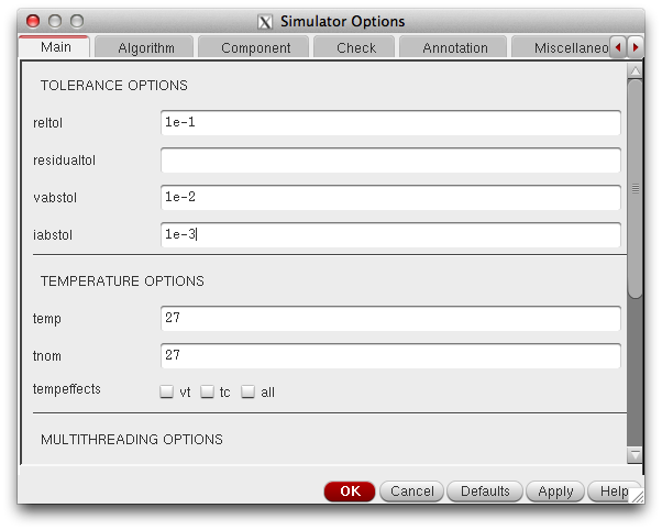
To Force Convergence: Simulation -> Options -> Analog (Ensure parameters match the image below)

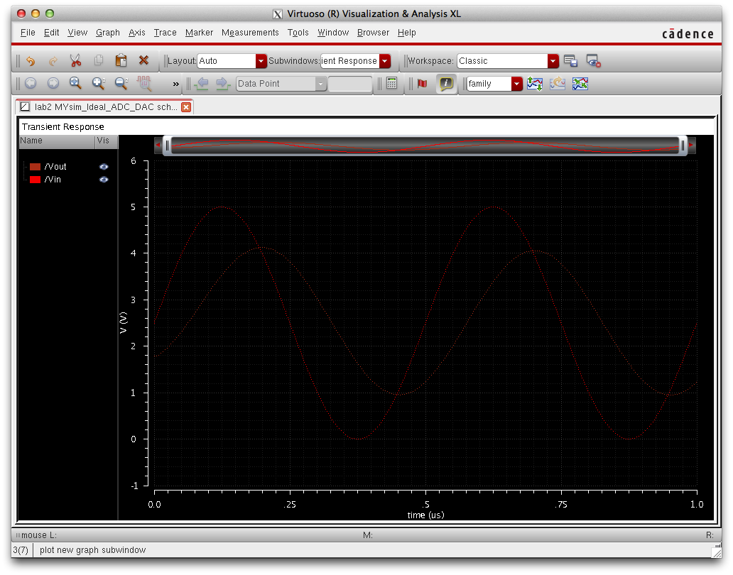
Simulation:


Simulation with a 10k resistor:


As you can see in the plot above, when adding a 10K resistive load the
output signal lost strength and decreased to about half of its original
input. As the load increases, the output's amplitude will continue to
get smaller. This shows how resistors can be used to manipulate
magnitude. Note that there are no horizontal shifts and the output
waveform is jagged due to there being no capacitive load.
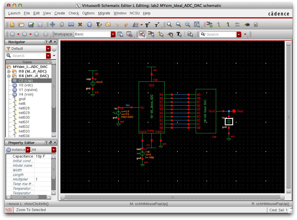
Simulation with a 10p capacitor:


Here we can observe that the capacitor 1. Smoothes out the output
signal and 2. Causes a phase shift (about 76ns as seen above). The
capacitor first off smoothes the signal making it look more like an
analog singal. Capacitors are often used to smooth out signals since
they act as a bucket that holds charge to maintain a constant flow of
current for output signals.
Simulation with a 10k resistor and 10p capacitor:


This plot shows an output signal phase shift of about 100ns, it can be
observed that amplitude of this signal is smaller than the output
signal with only a capacitive load and greater than the output signal
with only a resistive load.
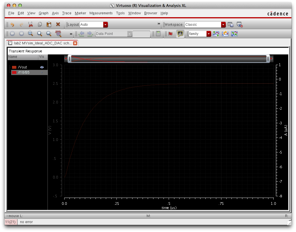
Caculating Delay:
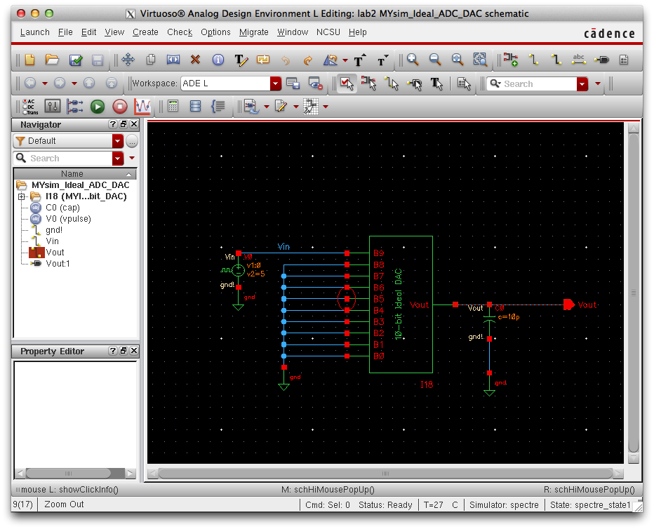
To calculate the delay we can take our DAC, ground all inputs except
for D9 and tie D9 to a pulse, add a 10pf capacitor to the output.
By using the formula .7RC we can predict a delay of 70ns= (.7)(10k)(10p), schematic and simulation shown below.
Remember delay is the time it takes for the output signal to reach half of it's peak amplitude.


Notes on total output resistance and output resistance when using MOSFETS:

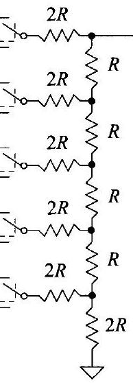
a)
To calculate output resistance, tie all inputs to ground, this would be
the same as tieing all switches in the above schematic to ground.
Now
we can calculate output resistance by adding resistance in parallel and
in series which in our circuit = R or approximately 10k.
b)
In a real circuit DAC's are implemented through the use of transistors
instead of resistors. MOSFET'S have a parasitic resistance,
if
this resistance is large compared to the resistance used for the
voltage divider of the DAC, the output voltage of the DAC will
decrease due to the voltage drop of the parasitic resistance. This is the same as replacing the switches in the image above with
resistors and tieing them to ground.
This is the end of Lab 2, back-up via email shown below:

