Lab 3 - EE 421L
Authored by Brian Kieatiwong
kieatiwo@unlv.nevada.edu
09/26/14
From the schematic of the resisitor divider created in Lab 1, we modify it for this lab.

After creating the schematic, we create the symbol for it.
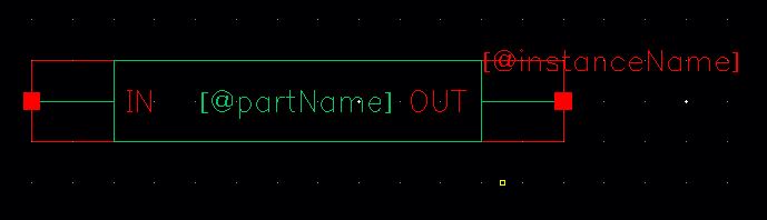
From
this symbol, we delete all the lines from the symbol except the the IN
and OUT pins. We then draw lines to create the symbol as seen below.

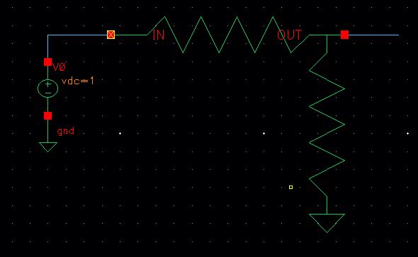
We then insert the newly created symbol into the schematic shown below.
Here,
we will create the layout for the resistor. Shown below is the layout
of the n-well layer. The dimensions of this layer are 56 um by 4.5 um.

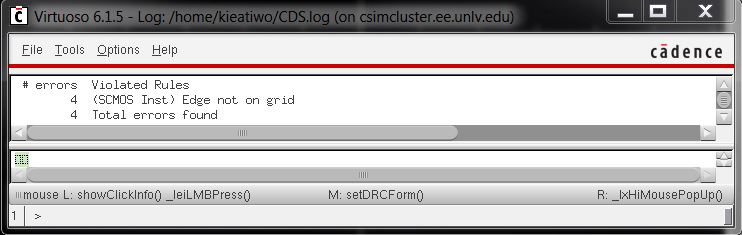
After
running a DRC, 4 errors are found. This error is due to the fact that
the layout edges do not touch the grids because the dimensions of this
layout must be in increments of 0.15 um. To fix this problem, the
length of the layout was increased to 56.1 um.
Be sure to copy all associated Lab 3 files into a backup folder of an external hard drive.
Return to EE421L Labs