Lab 5 - ECE 421L
Authored
by, Vincent Ibanez
Email: ibanez.troy.e@gmail.com
Today's
date 10/05/2014
PreLab:
Tutorial 3 – Design, layout, and simulation of a CMOS inverter
In this third tutorial I've drawn the schematic, symbol, and layout of a CMOS inverter.
I also simulated the DC behavior of the inverter.
I answered the following questions that were asked in the PreLab
1. What does the Bindkey q do?
Opens up the properties of a selected object
2. Which two Cell Views are used when doing an LVS?
Extracted and Schematic View
3. What is the difference between the nmos and nmos4 schematic cells?
In nmos, the body is assumed to be tied to ground
whereas in nmos4, it does not have the assumption.
4. How do you select the MOSFET models in the ADE window? What does ADE stand for?
Select setup>Model Libraries
5. What is the difference between moving and stretching?
Moving moves the selected object to a new location
whereas stretching changes the size of the selected object.
6. How do you layout a rectangle on the metal1 layer?
Press R while you have the metal 1 layer selected.
7. What does the ! indicate at the end of gnd! and vdd!
It is a global variable.
8. What do the acronyms LSW and CIW stand for?
Layer Selection Window, Command interperter Window
9. How is the ruler used? Cleared?
Press K, Shift+K
Let’s
start out, assuming Virtuoso has been started in the CMOSedu directory,
by copying the Tutorial_2 library to a library named Tutorial_3.
Ensure the new library is placed in $HOME/CMOSedu

Next create a schematic Cell View called inverter.

With this new schematic view open also open the schematic view of NMOS_IV.
What we are going to do is copy the NMOS symbol from the NMOS_IV cell into the inverter cell.
To do this we need to have both windows open (no clipboard that we can copy items to).
Press the copy Bindkey c (or
use the menu) then click on the nmos4 symbol and drag over into the
inverter window (and click the left mouse button to instantiate).

Close the NMOS_IV window and open the PMOS_IV window.
Repeat for the pmos4 cell to get the following.

Instantiate vdd and gnd supply nets.

Finally, wire up the inverter and add pins as seen below.
The A pin should have an input direction and pin Ai should have an output direction.

Next use the menu items to Create -> Cell View -> From Cell View to create the symbol for the inverter.
Check and Save the schematic view of the inverter (and then close this window).
Delete everything in the inverter’s symbol view except for the pins.
Draw the inverter symbol seen below (Create -> Shape -> Line/Circle)
Since
we aren’t showing the pin names select the pin and verify that it’s in
the right location (A is an input Ai is the inverter’s output)

Check and Save the inverter symbol.
Next Create the layout view for the inverter.

Add the following cells (nmos, pmos, ntap, ptap, and m1_poly) to this layout view as seen below (you can copy as before but here we will instantiate cells).
Ensure the nmos is 6u/0.6u and pmos is 12u/0.6u and the ntap and ptap use two columns.

Next align the cells until you get something similar to what is seen below.
DRC your layout to ensure no errors (fix as needed).
Save the layout.

Add rectangles on poly and metal1 as seen below.
DRC and save your design.


Next add pins on metal1 for gnd!, vdd! (both have a direction of inputOutput), A (input), and Ai (output).
DRC and save the design.

Next run extraction on the layout.

Finally, run the LVS on the inverter.


Okay, we are ready to simulate the operation of the inverter.
Create a cell called sim_inverter_dc (File -> New -> Cell View)
Draft the following schematic.
The symbol on the right is the no-connection symbol (in the basic library, Misc -> noConn) We add this symbol to be different and to avoid getting the warnings
related to floating pins/nets that we ignore via the menu items Check -> Find Marker -> ignore, ignore

Start the ADE and select the model files (Setup -> Model Libraries located in /$HOME/ncsu-cdk-1.6.0.beta/models/spectre/standalone)

Next select Analyses -> Choose
Note that the input vdc is named V0.

Next go to Outputs -> To Be Plotted -> Select On Schematic (select in and out)

Save the state in the cellview.
Netlist and Run the simulation (hit the green button).
We get the results seen below.
Note how the output is zero!
Well, we didn’t specify a vdd! anywhere so it should be zero. Let’s fix this.

Let’s add vdd symbol as seen below.

Check and Save the schematic.
Next, in the ADE, select Setup -> Stimuli and the parameters seen below (after hitting the Apply button).

Save the state (Cellview) so we don’t have to do this again next time we run the simulation.
Hit OK and run the simulation.
The results are what we expect the inverter voltage transfer curves to look like.

Let’s go ahead and simulate the extracted layout at this point (Setup -> Enviornment and add extracted in front of schematic as discussed in the last tutorial).

Which gives the same results as the schematic.
To verify we are simulating the extracted view and not the schematic view go to Simulations -> Netlist -> Display

Save and close everything. This concludes Tutorial 3.
Main Lab:
- In this lab we drafted the schematics, layouts, and symbols for two inverters having sizes of:
- 12u/6u (= width of the PMOS / width of the NMOS with both devices having minimum lengths of 0.6u)
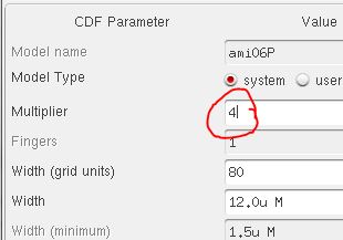
- 48u/24u where the devices use a multiplier, M = 4 (set along with the width and length of the MOSFET, image), as seen below
- I have also created symbols for the two inverters with different sizes.
- I have created layouts for both inverters as seen below.
- Notice that power is run on the top of the cell via metal1 and ground is run on the bottom of the cell also via metal1
- Power (vdd!) is connected to the n-well using the ntap cell
- Ground (gnd!) is connected to the p-substrate using the ptap cell
- Running power and ground with a single row of contacts, instead of 2 as seen below was done to reduce layout size
- Notice that the layout have 4 pins: A, Ai, vdd!, and gnd! (note how lowercase letters are used for power and ground)
- Both layouts for both inverters are also DRC checked


- The next image shows the extracted views obtained from the layouts above.


- After
extracting the schematic from the layout, both transistors are then LVS
checked to ensure that they are matching with the schematic plotted.


- Using SPICE, we simulated the operation of both of the inverters showing each driving a 100 fF, 1 pF, 10 pF, and 100 pF capacitive load
- The image below shows the schematic that was used to drive the 12u/6u inverter with different capacitive loads.
- The results of the simulation below was done using spice. The 12u/6u inverter is driving a 100f F capacitor.
- The results of the simulation below was done using spice. The 12u/6u inverter is driving a 1p F capacitor.
- The results of the simulation below was done using spice. The 12u/6u inverter is driving a 10p F capacitor.
- The results of the simulation below was done using spice. The 12u/6u inverter is driving a 100p F capacitor.
- Conclusion:
Notice that as the Capacitor value that the inverter is driving
increases, the delay for the inverted input to propagate to the output
increases. Hence, the inverter will have a limitation on how what
capacitance it can drive. For instance, in the 100p F capacitor seen
above, there is barely any inversion seen at all. This is of course,
assuming that we have a periodic input switching from 5v to 0v.
- The image below shows the schematic that was used to drive the 48u/24u inverter with different capacitive loads
- The results of the simulation below was done using spice. The 48u/24u inverter is driving a 100f F capacitor.
- The results of the simulation below was done using spice. The 48u/24u inverter is driving a 1p F capacitor.
- The results of the simulation below was done using spice. The 48u/24u inverter is driving a 10p F capacitor.
- The results of the simulation below was done using spice. The 48u/24u inverter is driving a 100p F capacitor.
- Conclusion:
Similar to the 12u/6u inverter, notice that as the Capacitor value that
the inverter is
driving increases, the delay for the inverted input to propagate to the
output increases. Hence, the inverter will have a limitation on how
what capacitance it can drive. For instance, in the 100p F capacitor
seen above, there is barely any inversion seen at all. This is of
course, assuming that we have a periodic input switching from 5v to 0v.
Also note that since our inverter is bigger due to a 4 multiplier set
in the parameter of both the nmos and pmos, the transistor can handle
driving larger capacitance a little better.
- The
above simulation were repated with UltraSim (Cadence's fast SPICE
simulator for larger circuits at the cost of accuracy).
- We used Setup -> Simulator/Directory/Host and select UltraSim as seen below
- We also pointed to the MOSFET models in Spectre.
- Note that UltraSim only performs transient simulations (not AC, Noise, DC, operating point, etc.)
- The results of the simulation below was done using UltraSim. The 12u/6u inverter is driving a 100f F capacitor.
- The results of the simulation below was done using UltraSim. The 12u/6u inverter is driving a 1p F capacitor.
- The results of the simulation below was done using UltraSim. The 12u/6u inverter is driving a 10p F capacitor.
- The results of the simulation below was done using UltraSim. The 12u/6u inverter is driving a 100p F capacitor.
- The results of the simulation below was done using UltraSim. The 48u/24u inverter is driving a 100f F capacitor.
- The results of the simulation below was done using UltraSim. The 48u/24u inverter is driving a 1p F capacitor.
- The results of the simulation below was done using UltraSim. The 48u/24u inverter is driving a 10p F capacitor.
- The results of the simulation below was done using UltraSim. The 48u/24u inverter is driving a 100p F capacitor.
-
In general, the results for both the Ultrasim simulation is a lot
similar to the Spice simulation with a little less accuracy of course,
for our purposes though, these differences are insignificant. Also notice that as the Capacitor value that
the inverter is
driving increases, the delay for the inverted input to propagate to the
output increases. Hence, the inverter will have a limitation on how
what capacitance it can drive. For instance, in the 100p F capacitor
seen above, there is barely any inversion seen at all. This is of
course, assuming that we have a periodic input switching from 5v to 0v.
Also note bigger inverters with higher multipliers can handle
driving larger capacitance, also they perform a little better in circuits that require high frequencies .
Finally, we backed up our design lab5vi.zip directory and other files for future study.
Return to labs


