Project - ECE 421L
Authored
by John Huang.
Huangj19@unlv.nevada.edu
November 8, 2014
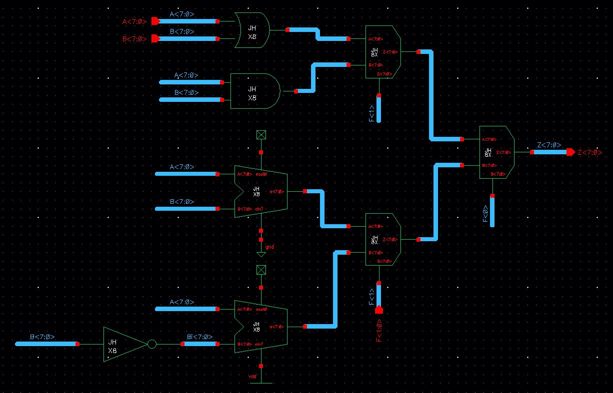
The schematic view of my 8 bit ALU.
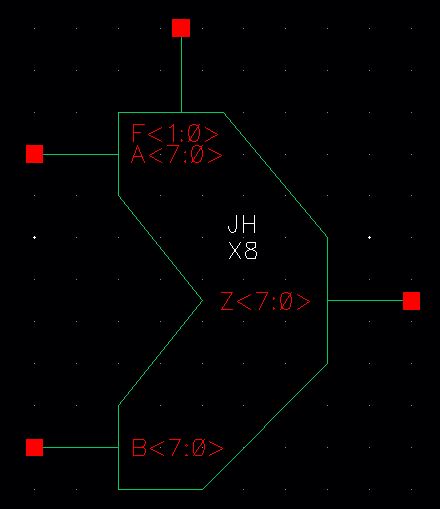
The symbol of my 8 bit ALU.
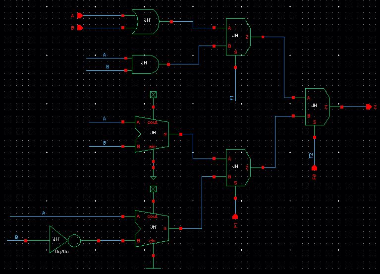
Simulations schematic.
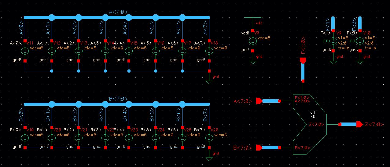
Input:
Logic gate order:
| F1 | F0 | OPERATION |
| 0 | 0 | SUBTRACTION |
| 0 | 1 | AND |
| 1 | 0 | ADDITION |
| 1 | 1 | OR |
Theoretical results:
| SUBTRACTION | 0 | 0 | 1 | 1 | 0 | 0 | 1 | 1 |
| AND | 0 | 0 | 1 | 0 | 1 | 0 | 0 | 0 |
| ADDITION | 1 | 0 | 1 | 0 | 0 | 1 | 0 | 1 |
| OR | 0 | 1 | 1 | 1 | 1 | 1 | 0 | 1 |
Experimental results:
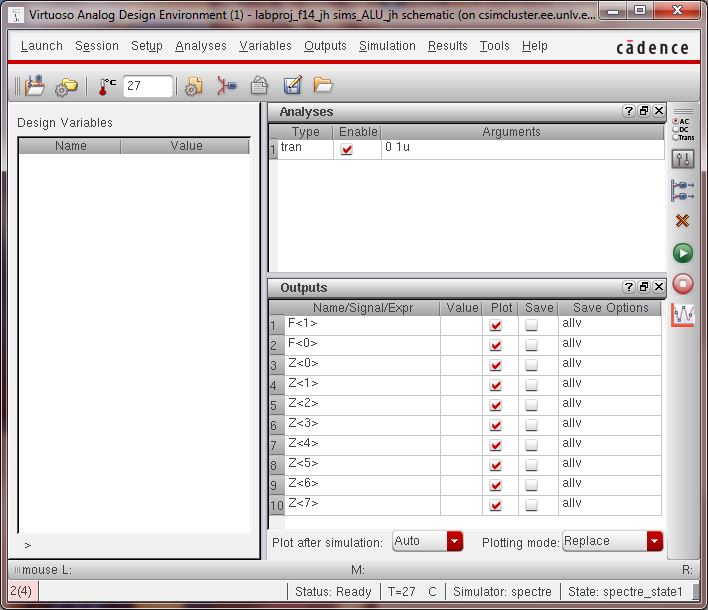
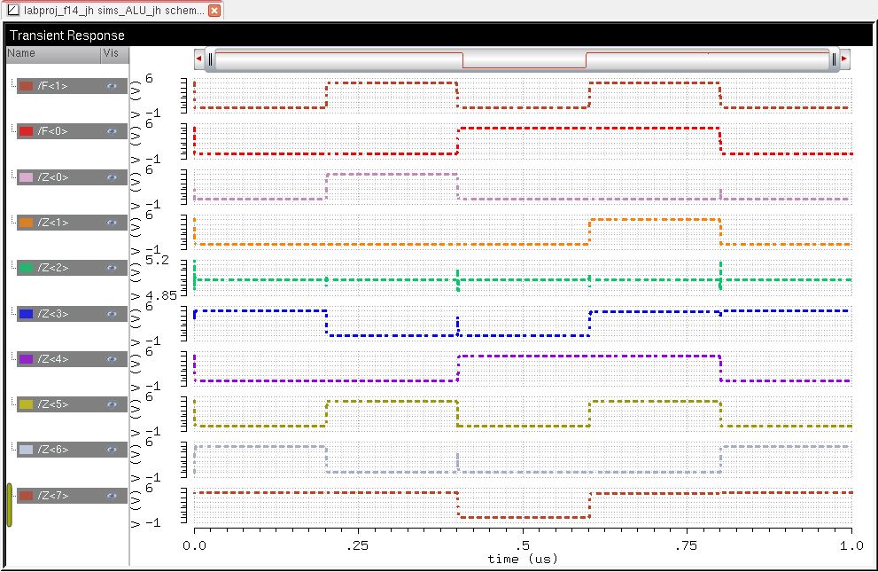
We can see that my experimental results match our theoretical results.
Now
for the layout, I simply created layouts for each of my gates only
using 1 bit gates. Making sure to DRC and LVS each layout to ensure
that there will be no mistakes when it came to laying out my 1 bit ALU.
6u/.6u Inverter layout
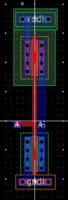
AND gate layout
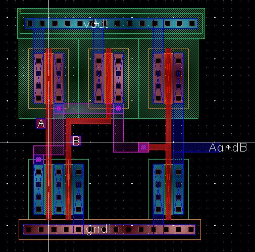
OR gate layout
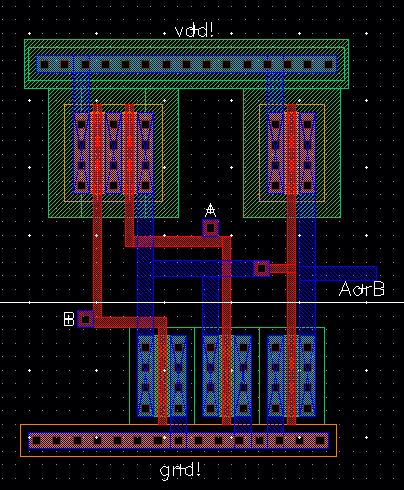
MUX layout
Full Adder layout
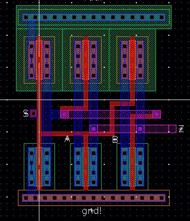
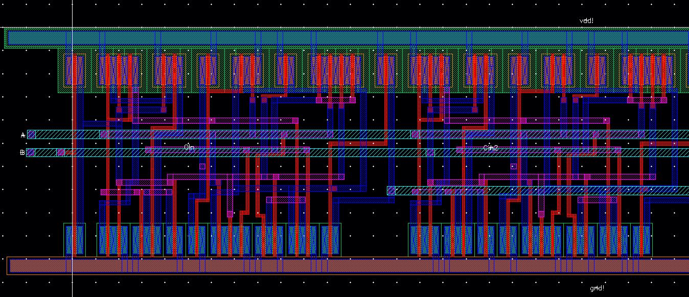
Using these single gate layouts, I created a 1 bit ALU layout and schematic.
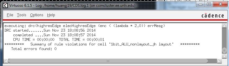
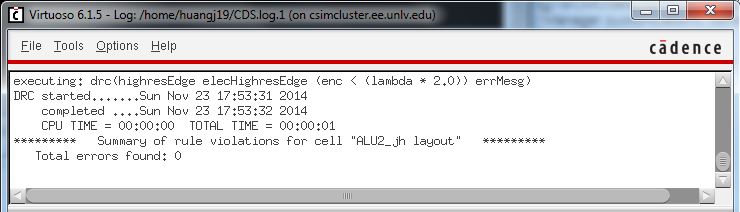
DRC:
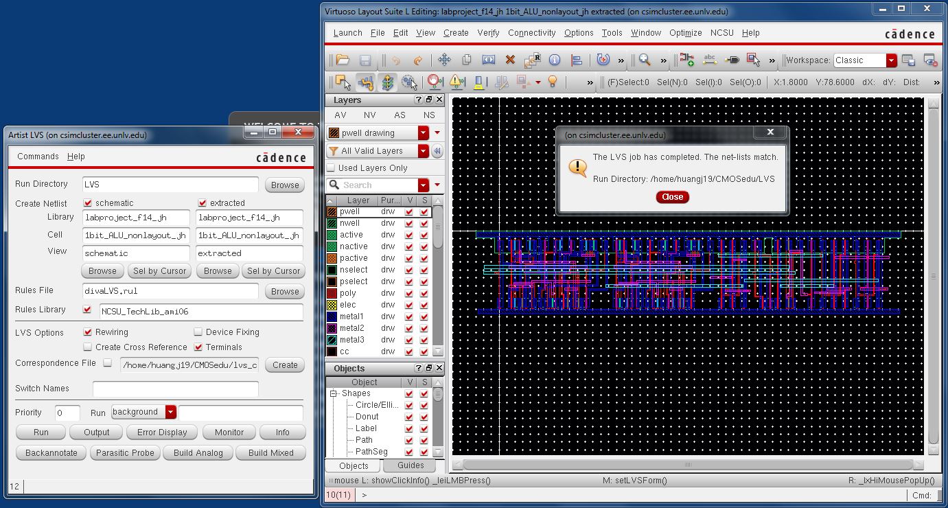
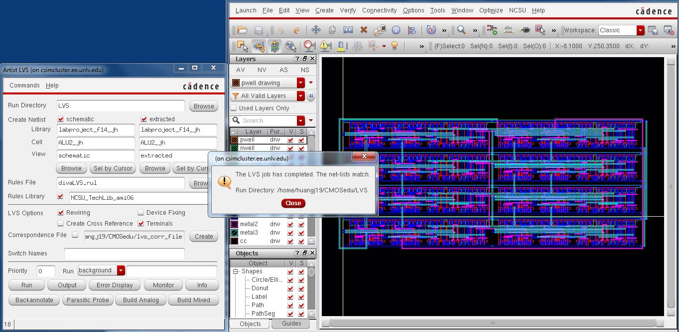
LVS:
After
making sure that these LVS. I edited the layout by copying the cellview
and removing the pin that has the Cin connected to vdd! and gnd! to
their respective full adders.
I needed to do this in order to instantiate the modified layout so I can interchain the Cin and the Cout's of each ALU.
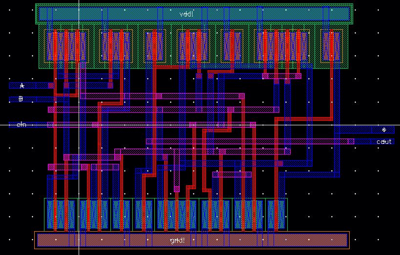
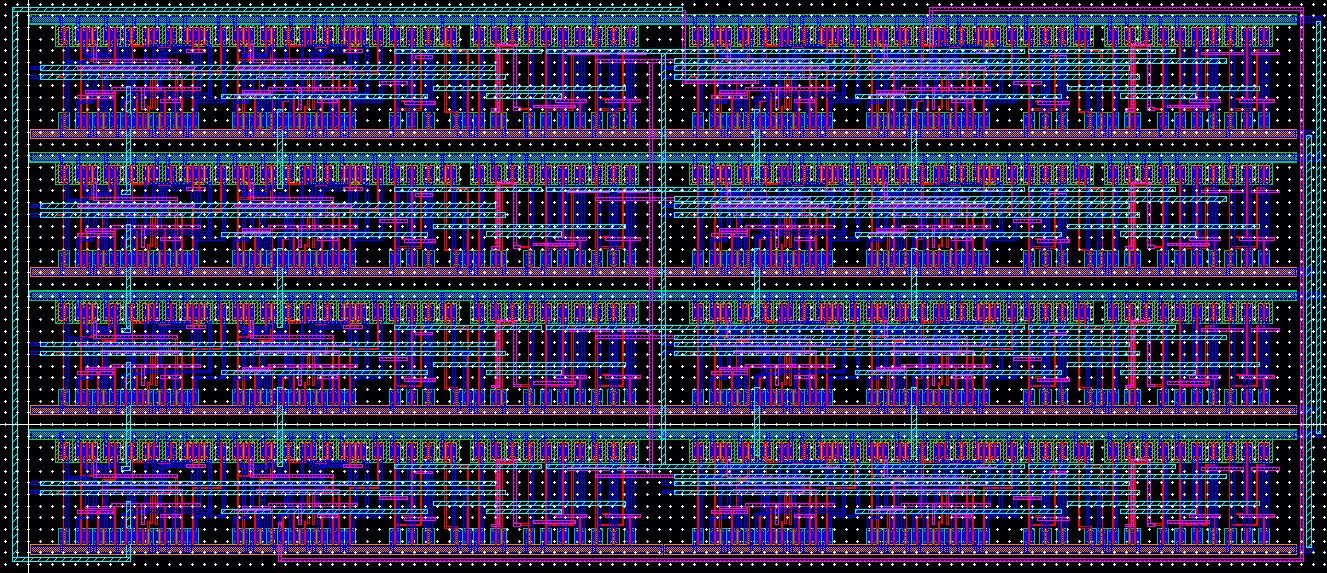
Then
instantiating 8 of my 1 bit ALU's. I connected all the vdd! and gnd!
together, along with all my F<0> and F<1> inputs and
finally my Cin to my Cout's together.
Creating new pins for each bit of my layout A<7:0>, B<7:0> and Z<7:0>.
Making sure that my layout DRC's.
And of course LVS!
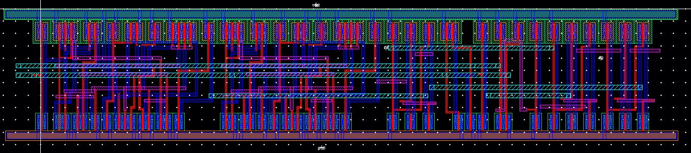
And the whole ALU is zipped up and placed here.
Zip up your labs and send them to yourself as back ups!

Return to EE 421L Labs