Lab 7 - ECE 421L
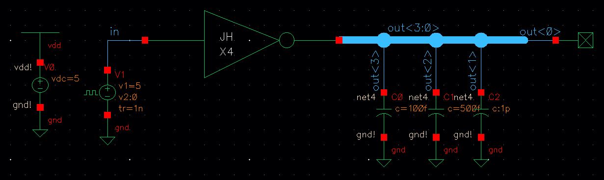
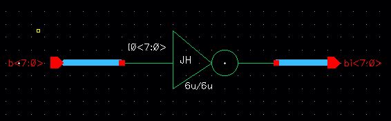
In this case it is a 4 bit array from 3 to 0.
We will also use wide wires meant for buses to implement the array.
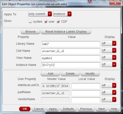
We create pins that correspond to the array number.
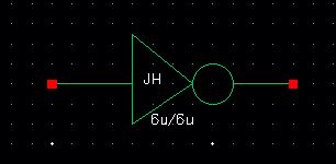
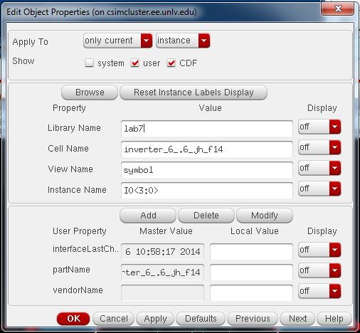
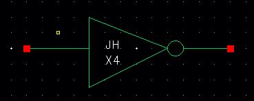
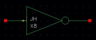
Using this schematic we can now create a symbol for a 4 bit inverter.
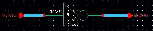
We can now simulate this 4 bit inverter with the following schematic.
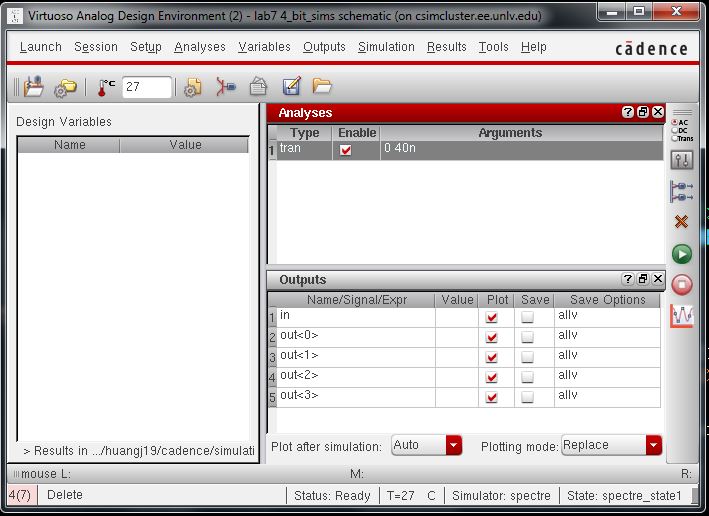
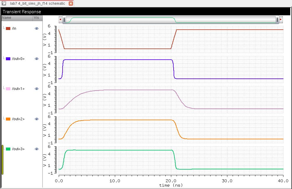
We will look at the process of all the gates at once after we create all our gates.
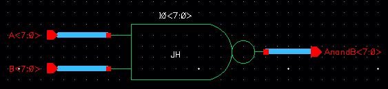
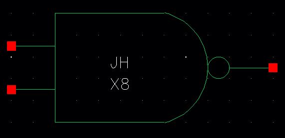
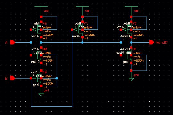
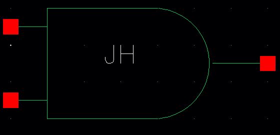
Now let's create a AND gate.
To do this we can simply add an inverter to our NAND schematic.
Then create a symbol from the AND gate.
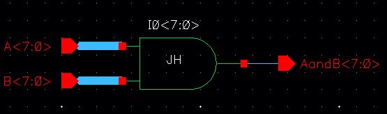
Now take the symbol and make it an 8 bit AND gate array.
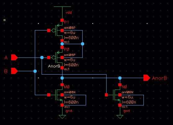
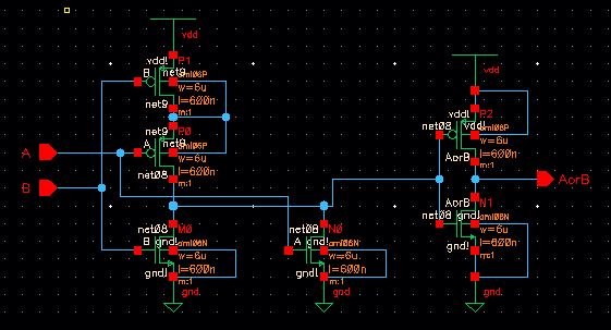
Now we can create a schemtic of the NOR gate.
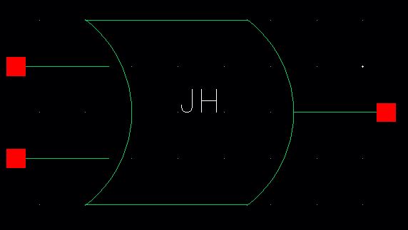
The symbol for the NOR gate.
Schematic for the 8 bit NOR array.
The symbol for the 8 bit NOR array.
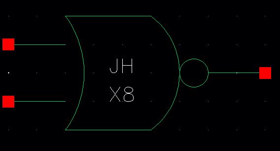
The symbol for the NOR gate.
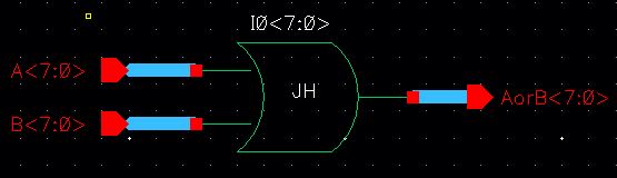
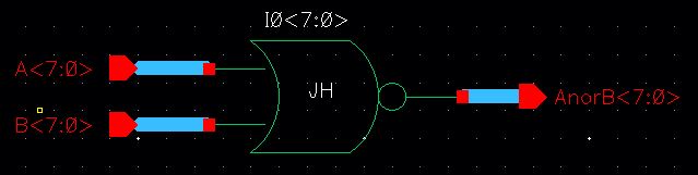
The schematic for the 8 bit NOR gate.
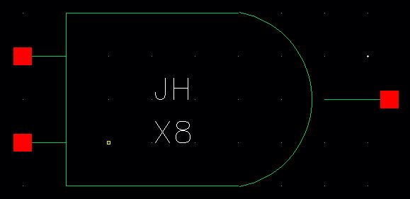
The symbol for the 8 bit NOR gate.
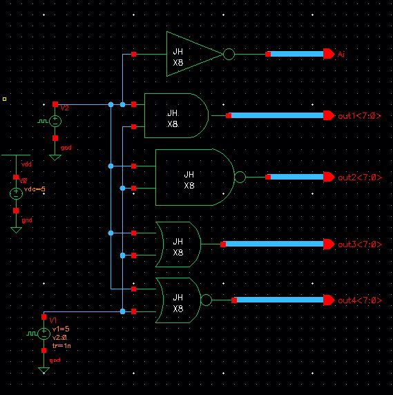
We can now simulate these gate arrays.
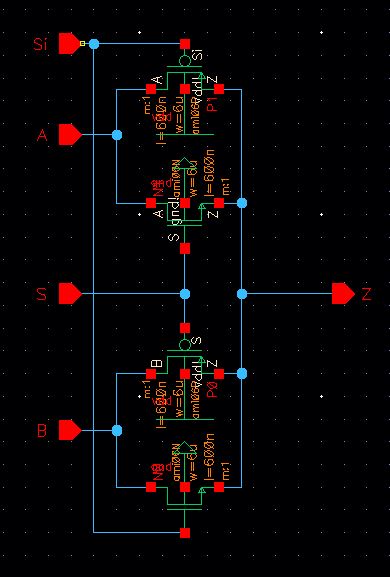
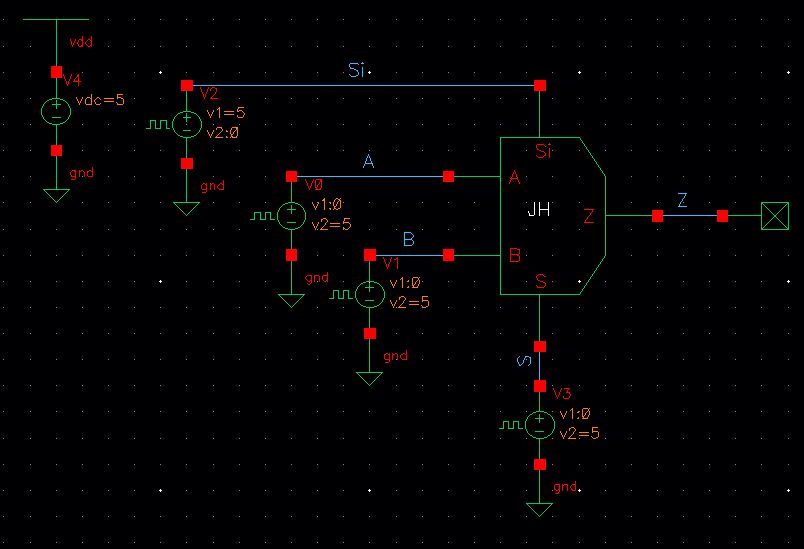
Now we can create a MUX.
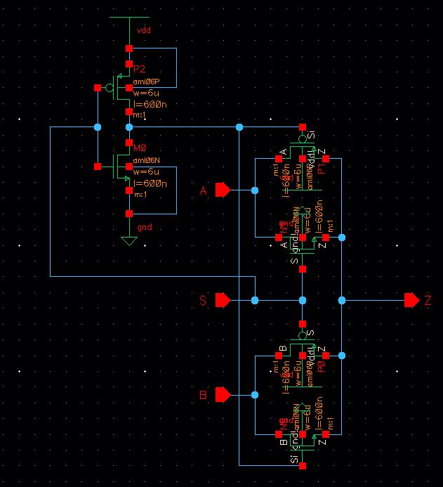
The schematic of the MUX.
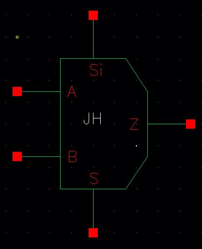
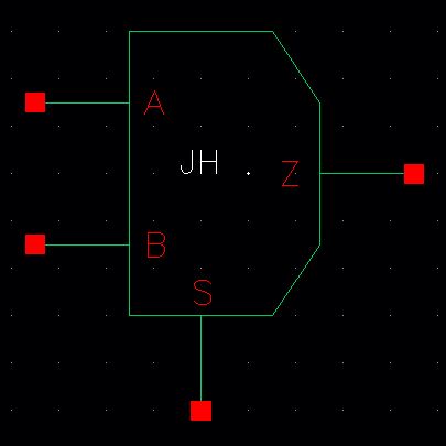
Creating a symbol for the MUX.
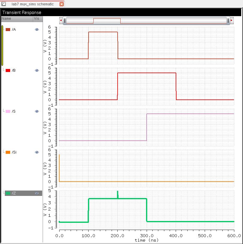
We can simulate our MUX symbol to see how it operates.
We can see in the graph that if depending on Si, the MUX will choose the value of A or B.
We can also create a DEMUX by adding an inverter for the S input feeding into the Si input.
Now we can create the DEMUX symbol from the schematic.
With the DEMUX symbol we can now make a 8 bit DEMUX symbol.
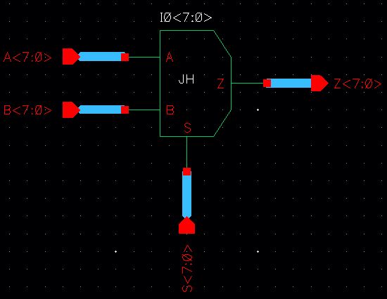
First the schematic of the 8 bit DEMUX.
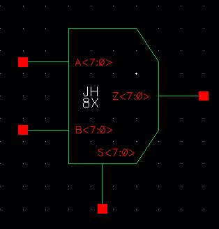
Then the symbol for the 8 bit DEMUX.
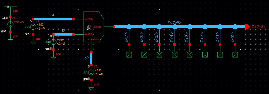
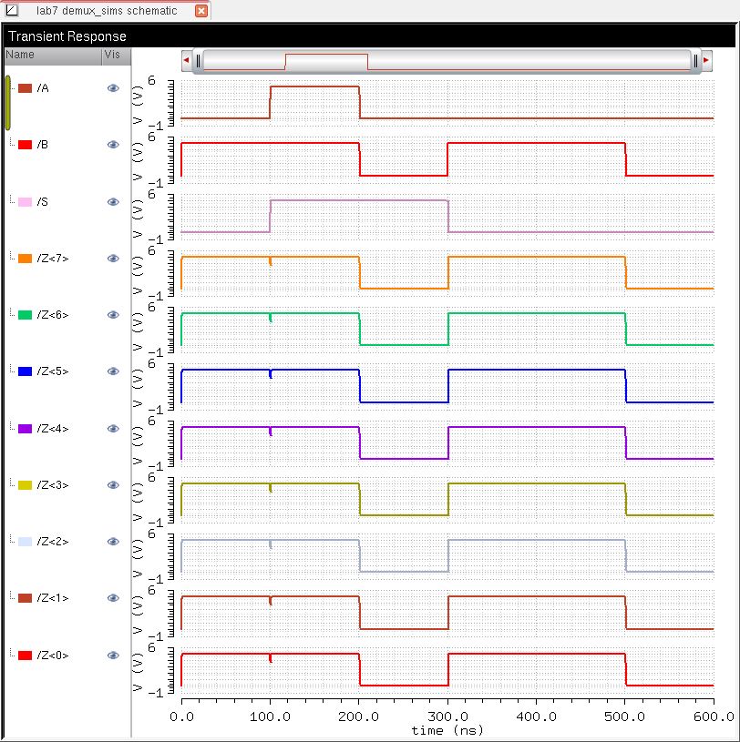
We can simulate our 8 bit DEMUX symbol to see how it operates.
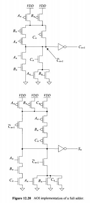
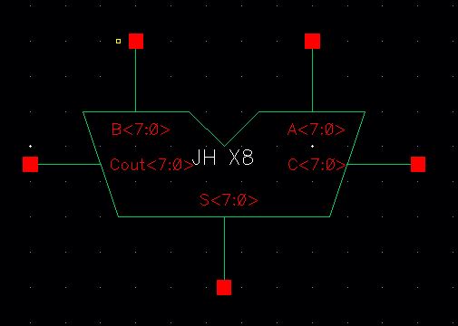
We are now going to recreate the full adder seen on Fig 12.20 from the CMOS book.
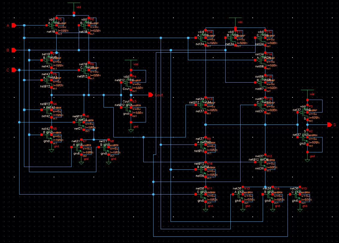
The schematic of the adder.
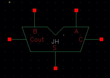
The symbol view of the adder.
The 8 bit adder schematic.
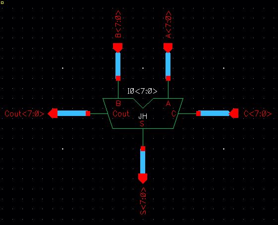
The 8 bit adder symbol.
The layout of a single adder.
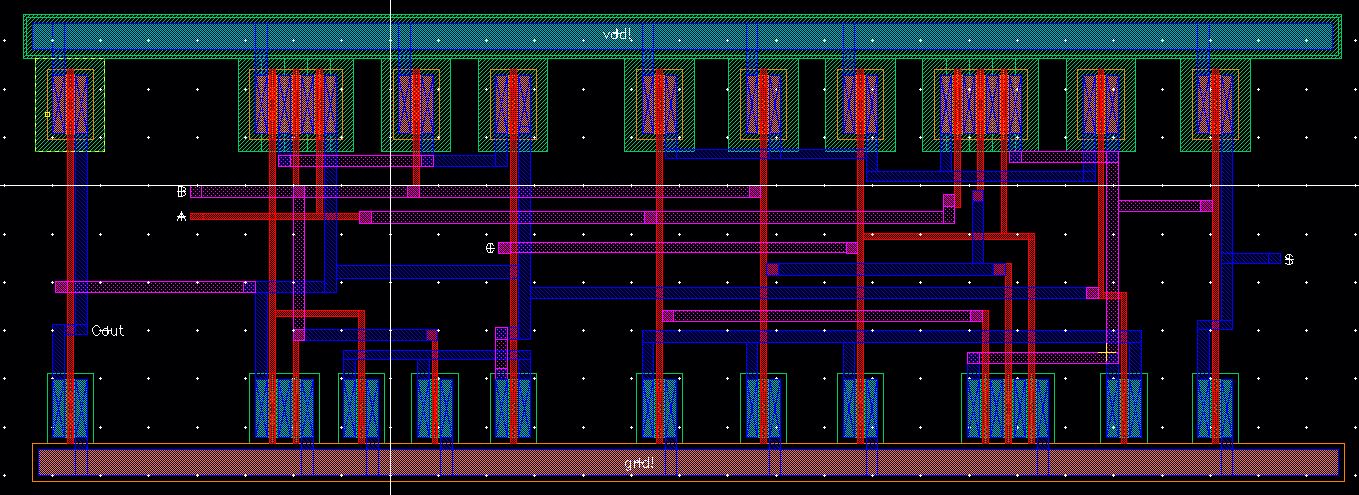
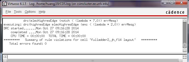
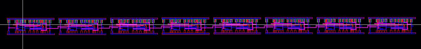
The 8 bit adder layout.